
Abstract
Tungsten trioxide (WO3) is one of the best transparent metal oxides for advanced technological applications. WO3 exhibits a wide variety of novel properties, particularly in thin film form. This investigation focuses on the morphological and optical properties of WO3 thin films prepared by electron beam deposition in an oxygen partial pressure of 2 × 10⁻⁴ mbar and at various substrate temperatures. The deposited films at room temperature (RT) are amorphous, but the crystallinity is enhanced by increasing the substrate temperature with noticeable x-ray diffraction peaks at (320), (210) and (402). The peaks represent the predominantly orthorhombic phase, with a portion of the hexagonal phase being included, of the WO3 films. The surface roughness and the grain size also increased as the substrate temperature increased. The optical transmittance and energy band gaps decreased with increasing substrate temperature. The band gap energy values were from 3.302 to 3.084 eV for the films deposited at substrate temperatures ranging from RT to 450 °C.
1 Introduction
Tungsten trioxide (WO3) is a transition metal oxide that exhibits structural transformations and sub-stoichiometric phase transitions. Tungsten trioxide exhibits a cubic perovskite like structure due to corner sharing of regular octahedra with the oxygen atoms at the corner and the tungsten atom at the center of each octahedron [Citation1]. WO3, in thin film form, has novel properties such as great optical modulation, good durability, and low power consumption [Citation2,Citation3]. Due to these properties, WO3 may be successfully used in electrochromic devices, display systems, variable reflection mirrors, gas sensors, optical memories, optical modulation, solar energy, writing–reading–erasing optical devices, flat panel displays, humidity and temperature sensors and microelectronic devices [Citation1,Citation4–Citation7]. Recently, the focus has been on devices that control light absorption, reflection and transmission such as chromogenic devices in which a reversible optical change can be induced by the influence of various stimuli. Of these, electrochromic devices can change optical properties continuously and reversibly under an applied electric field [Citation8].
WO3 is one of the best electrochromic materials with variable physical properties, such as by the deposition, crystallinity, structure, morphology and optical transmittance, that are enormously affected by deposition parameters like oxygen partial pressure and substrate temperature [Citation9]. Hence, this investigation studies the structural, morphological and optical properties of electron beam evaporated WO3 thin films at different substrate temperatures.
Tungsten trioxide can be deposited as a thin film using various deposition techniques, such as thermal evaporation [Citation1,Citation10,Citation11], electron beam evaporation [Citation12,Citation13], radio frequency (RF) sputtering [Citation14,Citation15], direct current (DC) magnetron sputtering [Citation6,Citation7], pulsed laser deposition [Citation16], chemical vapor deposition [Citation17–Citation19], Sol-gel technology [Citation20] and electrodeposition [Citation21], each having an effective use in scientific and technological applications. Each deposition technique produces a film with varied properties, such as composition, structure and morphology, on different substrates [Citation22]. For physical vapour deposition, the evaporation of the material due to resistive heating causes several disadvantages like low evaporation rates, and contamination. To avoid these disadvantages, electron beam evaporation was selected as an extensively used, simple, convenient and industrially viable alternative.
The aim of this work is to prepare WO3 thin films by electron beam evaporation at various deposition temperatures and characterize the films using their structural, morphological and optical properties.
2 Experimental details
2.1 Film deposition
WO3 thin films were prepared using electron beam evaporation which consists of a high power (3KW) electron beam gun operating at voltage of 5KV. 99.99% pure WO3 was obtained from Sigma-Aldrich. The powder was made into pellets with 1 cm diameters and 0.15 cm thicknesses, and these pellets were sintered at 1073 K for 7 hours. The films were deposited onto rectangular, optically flat, standard microscope slide substrates including well cleaned glass (from MICO), Si wafer, and ITO (from Sigma-Aldrich) coated substrates. The substrates were cleaned ultrasonically in acetone, washed with deionized water, and dried 20–30 minutes. The source to substrate distance was fixed at approximately 14 cm in a vacuum of 2 × 10⁻⁵ mbar under an oxygen partial pressure of 2 × 10⁻⁴ mbar at substrate temperatures of RT, 250 °C, 350 °C and 450 °C. The film thickness was controlled by both deposition rate (0.2 nm/sec) and deposition time (16–18 minutes). The thickness of the films was measured as 200 nm using a quartz crystal thickness monitor (built into the system). The WO3 pellet was placed in a graphite crucible and kept in the water cooled copper hearth of the electron beam gun. The pelletized WO3 targets were heated by an electron beam collimated from the d.c. heated tungsten filament cathode. The electron beam was bent by 2700 and the bended beam was incident on the pelletized WO3 target. The target surface was bombarded with the electron beam to deposit the film on the substrate.
During deposition, the material which is to be deposited is kept in a water-cooled hearth and the electron beam is produced by a hot filament. The process of evaporation takes place under a high vacuum to allow the target molecules to move freely in the chamber and then to condense on all surfaces including the substrates. The process of evaporation is divided into three stages. The primary stage is the heating of the hot filament, the second stage is the heating of the material that is to be deposited and the third stage is the vapor. After evaporation, the vapor is ready to move toward the wafer.
To examine the impact of substrate temperature on the structural, morphological and optical properties, the WO3 thin films were prepared by electron beam evaporation in an oxygen partial pressure of 2 × 10⁻⁴ mbar with substrate temperatures ranging from RT to 450 °C.
2.2 Characterization techniques
The physical properties of thin films are very sensitive to the film structure and surface morphology. Consequently, the structure of the films were analyzed using a Philips X-ray diffractometer (XRD) with a Cu Kα (λ = 1.5418 A0) target operated at 40 KV and 30 mA. The scanning angle 2θ was varied from 10-800 with a scanning speed of 2 deg/min in continuous scan mode. Atomic Force Microscopy (AFM) was used to detect microscale features on the film surface. The films, grown on ultrasonically cleaned glass substrates, are subjected to morphological studies using a NT-MDT Solver NEXT atomic force microscope. The surface morphology and grain size were also studied. The optical properties of thin films are vital for their practical application in electrochromic and photochromic devices. Hence, optical studies were completed for wavelengths of 300–1100 nm using a Shimadzu UV 1800 double beam Spectrophotometer.
3 Results and discussion
3.1 XRD Measurement:
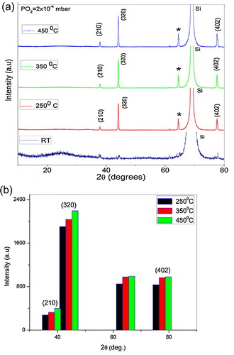
The structure of the WO3 thin films was analyzed using a Philips X-ray diffractometer with a Cu Kα (λ = 1.5418 A0) target between the scanning angles of 10-800 in continuous scan mode. The system was operated at a voltage of 40 KV and a current of 30 mA. . (a) shows the X-ray diffraction patterns of the WO3 thin films deposited by electron beam evaporation in an oxygen partial pressure of 2 × 10⁻⁴ mbar and at substrate temperatures ranging from RT to 450 °C. The XRD pattern for the film deposited at RT shows a broad hump near 2θ = 230, which indicates the amorphous nature of the film [Citation10]. As the substrate temperature was increased, the crystallinity of the films improves. The films deposited at substrate temperatures 250 °C, 350 °C and 450 °C, exhibited two crystal phases, namely hexagonal and orthorhombic phases, which are shown in . (a). The diffraction peaks (210) and (402) indicate a hexagonal phase (JCPDS 33-1387) with corresponding values of 2θ of 37.840 and 77.540, respectively. The inter planar spacing d-values were measured as 2.3880Ao and 1.2280Ao. The diffraction peak observed at (320) with 2θ at 44.080 indicates that the tungsten trioxide has an orthorhombic structure (JCPDS 20-1324) and corresponds to the d-value of 2.0560Ao. The peak at 64.440 marked with an asterisk shifts toward higher 2θ values as the substrate temperature increases. This peak is assumed to be a transitional phase from hexagonal to orthorhombic and leads to the orthorhombic phase. Among the peaks, (320) is the most intense peak which confirms the orthorhombic phase is predominant in WO3. Also, the intensity of the diffraction peaks increases with increasing substrate temperature and the peaks broaden [Citation16,Citation23]. The variation of the peak intensity with substrate temperature is shown in . (b).
Fig. 1 (a) XRD patterns of the WO3 films grown at substrate temperatures (Ts) from RT to 450 °C. (b) Intensity vs 2θ.
3.2 AFM Measurement
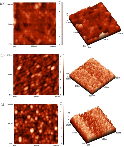
AFM is used to study the effect of substrate temperature on the surface morphology of the thin films. shows the two-dimensional (2D) and three-dimensional (3D) AFM images of the WO3 thin films deposited at substrate temperatures ranging from RT to 450 °C. The films deposited at RT have a smooth surface compared to the others which confirms its amorphous nature agreeing with Metin Usta [Citation11]. The surface roughness and grain sizes increase with increasing substrate temperature [Citation10]. The root mean square roughness increases from 1.8 to 4.20 nm and average grain size also increases from 42.5 to 86.52 nm as the substrate temperature is increased from RT- 450 °C. At higher substrate temperatures, atoms agglomerate on the surface which may cause the formation of large grains.
Fig. 2 AFM images of the WO3 thin film with substrate temperatures of (a) Ts = RT, (b) Ts = 250 °C, (c) Ts = 350 °C and (d) Ts = 450 °C, under a PO2 = 2 × 10⁻⁴ mbar.
3.3 Optical properties
. (a) displays the optical transmission spectra of the WO3 thin films prepared at an oxygen partial pressure of 2 × 10⁻⁴ mbar with substrate temperatures ranging from RT – 450 °C. The films prepared at room temperature have a transparent bluish color indicating the amorphous nature of the films. The relatively high transmittance of these films are due to their feeble absorbance. The increase in the peak in . (a) at wavelengths shorter than 300 nm was unexpected and is due to the instrument default, which can be ignored. The transmittance of the films decreases slightly at the fundamental absorption edge at approximately 350 nm, and the transmittance also decreases with increasing substrate temperature. This may be attributed to oxygen deficiencies present at higher substrate temperatures [Citation10]. This leads to higher charge carrier concentrations and hence the free carrier absorption of light increases with substrate temperature.
Fig. 3 (a) Transmission spectra of the WO3 films deposited at different substrate temperatures (Ts). (b) (αhυ)1/2 versus hυ plots for WO3 thin films deposited at different substrate temperatures (Ts).
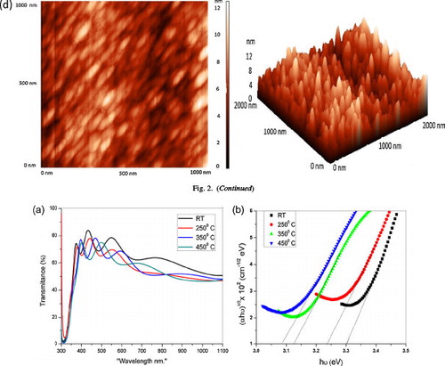
The optical absorption coefficient of these films was evaluated using the relation, [Citation24]α = 1/t ln[T/(1-R)2] where T is the transmittance, R is the reflectance and t is the film thickness. The optical absorption coefficient of the WO3 films at the fundamental absorption edge is exponentially dependent on the photon energy. The exponential dependence of the optical absorption coefficient may arise from the electronic transitions occurring between localized states, which tail off in the band gap. For incident photon energies greater than the band gap and above the exponential, the optical absorption follows a power law, [Citation10,Citation25](αhυ) = β (hυ − Εg)n where hυ is the incident photon energy, β is the edge with parameter and n is an exponent. The exponent, n, determines the type of electronic transitions causing the absorption and has the values 1/2, 3/2, 2 and 3 for direct allowed, direct forbidden, indirect allowed and indirect forbidden transitions, respectively [Citation10,Citation26].
The deposited WO3 thin films gave a suitable fit for n = 2, as shown in . (b), which indicates an indirect allowed transition like those reported by Vemuri [Citation27] for sputtered WO3 thin films. The extrapolation of the straight-line graph from α1⁄2 = 0 gave a value for optical band gap ‘Eg’. The optical energy band gap value for the films deposited at room temperature is 3.302 eV. The estimated bandgap value for the films deposited at room temperature is marginally higher than the reported value of 3.25 eV by Deb [Citation28]. The optical energy band gap (Eg) diminished from 3.302 – 3.084 eV when the substrate temperature increased from RT to 450 °C. [Citation10,Citation16,Citation29]. The reported band gap for the films deposited at 250 °C is approximately the same as the value reported by Nakamura [Citation30] with the same pattern of diminishing bandgap values. These values are also in agreement with the thinner films deposited using CVD by Davazoglou [Citation31].
4 Conclusions
The structural, morphological and optical properties of the WO3 thin films deposited by electron beam evaporation were strongly dependent on the substrate temperature. The XRD and AFM studies showed that the structure and morphology of the films could be changed by the substrate temperature. The films deposited at RT are amorphous and an increase in crystallinity occurs as the substrate temperature increases from 250 – 450 °C. The XRD peaks at (320), (210) and (402) represent the mixed orthorhombic and hexagonal phases of the WO3 thin films. The peak at (320) is the most predominant, confirming the orthorhombic phase of WO3. From the AFM studies, the surface roughness and grain sizes were observed to increase with increasing substrate temperature. The transmittance of the films decreased slightly at 350 nm coinciding with the fundamental absorption edges. The optical energy band gap, Eg, decreases from 3.302-3.084 eV as the substrate temperature increases from RT-450 °C.
Acknowledgement
This work was supported by the Department of Science & Technology (DST-SB/FTP/ETA-43/2013), New Delhi India.
Notes
Peer review under responsibility of Taibah University.
Related Research Data
References
- M.C.RaoO.M.HussainRes. J. Chem. Sci.1Oct. (7)20117678
- E.S.LeeD.L.DiBartolomeoSol. Energy Mater. Sol. Cells712002465
- K.Hari KrishnaO.M.HussainC.GuillenOptoelectronics and Advanced Materials–Rapid Communications2Apr. (no. 4)2008242246
- Y.A.YangJ.N.YaoJournal of Physics and Chemistry of Solids612000647650
- GuangzhongXieJunshengYuXiChenYadongJiangSensors and Actuators B1232007909914
- A.SubramanyamA.KaruppasamySolar Energy Materials & Solar cells912007266274
- A.KaruppasamyApplied Surface Science3592015841846
- C.G.GranqvistHandbook of Inorganic Electrochromic Materials1995Elsevier ScienceAmsterdam reprinted (2002)
- K.MasekJ.LibraT.SkalaM.CabalaV.MatolicV.ChabK.C.PrinceSurface Science60020061624
- K.J.PatelC.J.PanchalV.A.KherajM.S.DesaiMaterials Chemistry and Physics1142009475478
- MetinUstaSuleymanKahramanFatihBayansalHaci A.CetinkaraSuperlattices and Microelectronics522012326335
- A.A.JoraidS.N.AlamriPhysics B.3912007199205
- R.SivakumarR.GopalkrishnaM.JayachandranC.SanjeevirajaOptical Materials.292007679687
- M.StankovaVilanovaE.LlobetJ.CaldererC.BittencourtJ.J.PireauxX.CorreigSensors and Actuators B1052005271277
- CelineLemireDava B.B.LollmanAhmadAl MohammadEvelineGilletKhalifeAguirSensors and Actuators B842002
- K.J.LethyD.BeenaR.Vinod KumarV.P.Mahadevan PillaiV.GanesanVasant SatheApplied Surface Science254200823692376
- P.TagtstromU.JanssonThin Solid Films3521999107113
- K.L.HardeeA.J.BardJ. Electrochem. Soc.1241977215224
- J.M.BerakM.J.SienkoJournal of Solid State Chemistry21970109133
- MasoomehSharbatdaranAbdoljavadNovinroozNoorkojaouriIron. J. Chem. Chem. Eng.220062529
- G.LeftheriotisP.YianoulisSolid State Ionics179200821922197
- S.S.KalagiS.S.MaliD.S.DalaviA.I.InamdarH.ImP.S.PatilElectrochmica Acta852012501508
- O.AlmL.LandstromM.BomanC.G.GranqvistP.HeszlerAppl. Surf. Sci.2472005262267
- K.J.ChopraThin film Phenomena1969Mc Graw-HillNew yark p. 734
- N.KennyC.R.KannewurtS.H.WhitemoreJ.PhysChem. Solids2719661237
- E.A.DavisN.F.MottPhil. Mag.221970903
- R.S.VemuriM.H.EngelhardC.V.RamanaApplied Materials Interfaces4201213711377
- S.K.DebPhilosophical Magazine271973801822
- K.MiyakeH.KanekoM.SanoN.SuedomiJ. Appl. Phys.5519842747
- A.NakamuraS.YamadaAppl. Phys.2419815559
- D.DavazoglouG.LevequeA.DonnadieuSolar Energy Materials171988379390