
 ?Mathematical formulae have been encoded as MathML and are displayed in this HTML version using MathJax in order to improve their display. Uncheck the box to turn MathJax off. This feature requires Javascript. Click on a formula to zoom.
Abstract
The paper reports the role of Ag additives on light induced metastable defects in Se–In glassy alloys using a well-known thermally stimulated current (TSC) technique. Amorphous thin films of Se90In10−xAgx (x = 0, 2, 4, 8) were prepared by thermal evaporation. Measurements were made in the given thin films prior to and after exposing amorphous thin films to white light for different exposure times (0–1.5 hrs). The density of light induced metastable defects increases with exposure time, and the fractional increase in light induced metastable defect density decreases as Ag concentration increases.
1 Introduction
Chalcogenide materials are intrinsically metastable, because they can attain a long range order, and the structure can be easily changed from one metastable state to another due to structural flexibility. The most interesting property of these materials is how light illumination affects them. These materials show a variety of light induced effects [Citation1,Citation2], which may be due to changes in volume, optical constants, optical band gap, refractive index, optical absorption coefficient or density. The primary effects are photo-induced anisotropy [Citation3], photo crystallization [Citation4], photo contraction [Citation5], photo expansion [Citation6], photo volumetric changes [Citation7], photo-induced amorphization [Citation8], photo vaporisation [Citation9], photo diffusion [Citation10], photo polymerisation [Citation11], photo darkening [Citation12], photo bleaching [Citation13], change in elastic constants [Citation14], and photodecomposition [Citation15]. Some of these light-induced effects are due to light induced metastable defects. Therefore, the study of these defects is a very interesting problem in the case of chalcogenide glassy semiconductors.
Table 1 Values of trap density and fractional increases for various exposure times in a-Se90In10 thin films.
Table 2 Values of trap density and fractional increases for various exposure times in a-Se90In8Ag2 thin films.
Table 3 Values of trap density and fractional increases for various exposure times in a-Se90In6Ag4 thin films.
Table 4 Values of trap density and fractional increases for various exposure times in a-Se90In2Ag8 thin films.
Recently, Se-based chalcogenide glasses have become more important from a research and application point-of-view. Several researchers [Citation16–Citation18] have found that Se-based glasses are more useful than pure Se due to higher photosensitivity, greater hardness, higher crystallization temperature and a lower ageing effect. Matsushita et al. [Citation18] observed that a Se–In binary glassy system was very interesting for applications in solar cells. Various researchers have also reported that some metallic additives change the conduction from p-type to n-type in Ge–Se and Se–In glassy systems [Citation19]. Therefore, the study of these glassy systems is very important.
Frumar and Wagner [Citation20] reported that chalcogenide glasses containing Ag change the electrical conductivity of the glasses by several orders of magnitude. The electrical and optical properties of Ag-doped chalcogenide glasses have been studied [Citation21,Citation22]. These glasses have many potential applications [Citation23] in optoelectronics, basic sciences, cell devices, optical elements, gratings, optical memories, micro-lenses, waveguides, biological and electrochemical sensors, solid electrolytes and batteries, among others. Recently, it has been reported that a variety of light induced effects are also observed in these glasses [Citation24–Citation26].
The present communication reports the role of Ag additives on light induced metastable defects in a Se–In chalcogenide glassy system. The thermally stimulated current (TSC) technique has been used here to quantitatively estimate light induced metastable defects.
2 Experimental details
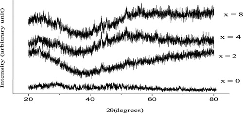
Glassy alloys of Se90In10−xAgx (x = 0, 2, 4, 8) are prepared by the well-known melt quenching technique. High purity 5 N materials are sealed in quartz ampoules (length ∼5 cm and internal diameter ∼8 mm) in a vacuum, ∼10−5 Torr. The ampoules containing the high purity 5N material in vacuum are held in a furnace at 900 °C for 12 hrs, where the ampoules are constantly rocked to make the melt homogeneous. The melt is rapidly cooled by removing the ampoules from the furnace and dropping them into ice-cooled water. The quenched samples are removed from the ampoules by breaking the quartz ampoules. The X-ray diffraction (XRD) pattern of the prepared sample, having no sharp peaks, confirmed the amorphous nature of present system, as shown in .
Fig. 1 X-ray diffraction pattern of Se90In10−xAgx (x = 0, 2, 4, 8) glassy alloys.
Thin films of glassy alloys are prepared by the vacuum evaporation technique, maintaining the glass substrates at room temperature. Vacuum evaporated indium electrodes at the bottom are used for electrical contact. The thickness of the film is ∼500 nm. The films are maintained in the deposition chamber in the dark for 24 hrs before mounting in the sample holder to allow sufficient annealing at room temperature so that a metastable thermodynamic equilibrium may be attained in the samples.
For thermally stimulated current (TSC) measurements, thin films are mounted in a specially designed sample holder containing a transparent window for shining light; a vacuum of 10−2 Torr is maintained throughout the measurements. The temperature of the film is measured by a calibrated copper constantan thermocouple mounted very near to the film. The films were annealed at approximately 360 K for one hour in a vacuum of 10−2 Torr before the measurements. To expose the films to 1200 lux white light for different exposure times, a 200 W tungsten lamp is used as light source. Light intensity is measured by a digital lux metre. Proper care was taken to avoid the thermal effects of light so that the temperature of the film does not change significantly.
The temperature dependence of the thermally stimulated current (TSC) is measured in two states at a fixed voltage of 100 V in the ohmic region. In state −I, the sample is heated at a constant heating rate from room temperature, 300 K–368 K without any light exposure; the current is measured during heating. However, the state-II sample is heated with the same heating rate after two minutes with the light shining at room temperature; the decay of photoconductivity was allowed for 10 minutes after switching off the light to allow sufficient time for decay. The difference of currents of these two states the TSC and plotted as a function of temperature to generate the TSC curve.
3 Results and discussion
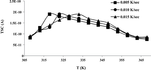
The experimental TSC curves are generated for Se90In10−xAgx (x = 0, 2, 4, 8) thin films at different heating rates (0.005 K/Sec, 0.010 K/Sec, and 0.015 K/Sec). shows TSC curves from Se90In6Ag4 (similar results are obtained for other samples). From this graph, it is clear that the TSC peaks shift to higher temperatures as the heating rate increases. Shifts of this peak as a function of heating rate confirm the observations of TSC [Citation27] that were also observed other researchers [Citation28,Citation29] in chalcogenide glasses. To study the effect of prolonged exposure to light, TSC measurements were made before and after exposing the samples for different exposure times. To study the effects of prolonged exposure to light, TSC measurements were first made at different exposure times at a heating rate of 0.010 K/Sec.
Fig. 2 Experimental TSC curve of a-Se90In6Ag4 thin films at various heating rates.
This was performed to observe changes in the density of defect states due to light exposure. The trap density was calculated using the area of the TSC curve from the following equation [Citation30]:(1)
(1) where Q represents the quantity of the charge released during the TSC experiment. This can be calculated from the area under TSC peak. L and A are the thickness and area of the sample, respectively, e is the electronic charge and G represents the photoconductivity gain estimated using the expression [Citation31]
(2)
(2) where τ represents the carrier life time, and ttr represents the carrier transit time between electrodes. In the present TSC measurements, the carrier life time and carrier transit time values were not measured; the carrier life time and carrier transit time were assumed to be equal, which is the same assumption as previous researchers for a-Si-H and chalcogenide glasses [Citation32,Citation33]. Thus, using Eq(2), the conductivity gain (G) was taken to be 1 for the present measurements.
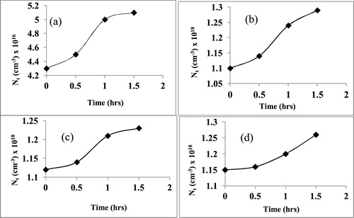
The TSC curves from the Se90In6Ag4 thin films for different exposure times (0, 0.5, 1, 1.5 hrs) are plotted in , and similar results are obtained for other samples x = 0, 2, 8 in Se90In10−xAgx. Trap density was evaluated using equation Equation(1)(1)
(1) , and the results are given in – for various compositions. (a–d) demonstrates the concentration of trap density as a function of exposure time for the Se90In10−xAgx (x = 0, 2, 4, 8) glassy system. From these figures, it is clear that trap density increases with the increasing of exposure time of light for all the samples. Comparing these results to previous results in the field, D. K. Biegelsen and R.A. Street [Citation34] have observed that due to optical irradiation, the generation of coordination defects in chalcogenide glasses oppose the excitation of pre-existing defects. They also suggested light induced electron spin resonance (LESR) experiments in which self-trapped excitons, that is, conjugate pairs of charged defects, are induced by light exposure. The formation of a self-trapped exciton (STE) state is symmetric, and such STE states do not act as trapping centres for electrons or holes because they are effectively neutral; therefore, they do not affect prolonged exposure conductivity. Alternatively, random pairs (RP) of D+, D− defects may result from bond switching reactions at STE centres, therefore, acting as electron or hole trapping centres would act to decrease prolonged exposure conductivity.
Fig. 3 TSC curve of a-Se90In6Ag4 thin films at various exposure times (0, .5, 1, 1.5 hrs).
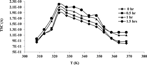
Fig. 4 Variation of trap density as a function of exposure time for (a) Se90In10, (b) Se90In8Ag2, (c) Se90In6Ag4 and (d) Se90In2Ag8 thin films.
Shimakawa et al. proposed a microscopic model for LIMD creation [Citation35,Citation36]. This model has explained many photo-induced phenomenon. The initiation of defect creation was assumed to be the formation of STE in the form of intimate alternation pair (IP), which is stable at lower temperatures. Accordingly, fatigue of the primary peak accompanying the low energy peak and a part of LESR can be related to this Ips, since these phenomena are completely removed by annealing approximately 300 K. Following this, defect conserve bond switching, which is increased by light exposure leading to defect separation and migration, results in the formation of metastable well-separated charged defects known as random pairs (RP). These RPs are only removed by annealing near the glass transition temperature. These RPs dominate photoconductivity as recombination centres, and these IPs and RPs are increase AC transport [Citation35,Citation37].
In the charged defect model or the valence alternation pair model, bonding defects can have three charged states, which are denoted by D+, D− and D0, where D denotes the defect state or a dangling bond, and the superscript denotes the respective charge states. The neutral dangling bond D0, for example, a singly coordinated chain-end Se atom, would normally possess spin, but it is unstable [Citation38]. Here, the photo-induced creation of D0 centres from normal bonding state (NB) first occurs, and it is important that the energy minimum of the photoexcited state is located above the D0 centres. These D0 centres are considered to be quasi stable, and the decrease in photocurrent with the exposure time observed at room temperature can be related to the creation of D− and D+ from D0 centres. In this case, the existence of D+ centres is not essential here, and the D− centre can be transferred from the D0 centre at room temperature according to the following equation:where h denotes hole. These photo-induced charge defects are metastable and can be removed by annealing near the glass transition temperature.
Ovshinsky and Adler [Citation39] explained the importance of the interaction between the lone pair electrons of the chalcogenide atoms that belong to different segmental and/or fragmental clusters. The quasi stable states D0 and D− can be replaced by the structures D1 and D2, respectively. Upon illumination with light in chalcogenide glasses, the electron hole pair is excited, the hole can diffuse, and the electron is left behind, which is less mobile.
The hole may be captured by a hole trap, which, in turn, traps by modifying intercluster interactions, that is, the lattice relaxation occurs at room temperature. Thermal energy can excite the trapped electrons, leaving the atomic structure unchanged. The electrons can diffuse, and it can recombine with the trapped hole. In the present case, the atomic structure of the hole trap will be partially relaxed; therefore, the number of hole traps increases, which causes the decrease in the photocurrent as a function of exposure time during illumination.
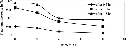
We observed an increase in the density of defects with light shining at room temperature. These defects may act as traps and affect thermally stimulated currents. The observed defects could be random pairs, as suggested by Shimakawa et al. [Citation40]. The fractional increase in the density of traps due to light exposure has been calculated for each exposure in all alloys studied, and the results are shown in – and plotted in .
Fig. 5 Fractional increase in Nt vs. light exposure time for Se90In10−xAgx (x = 0, 2, 4, 8) thin films.
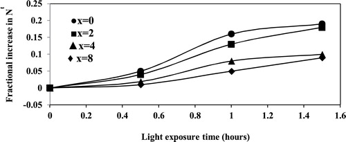
These results demonstrate that fractional increases in trap density decreases as Ag concentration increases (See ). Thus, light induced metastable defects decrease as Ag concentration increases in the Se–In glassy system; hence, Ag doped materials are suitable for optoelectronic device applications. In our previous communication [Citation41] estimating light induced defects in the same samples, the space charge conduction technique was used, and similar results were obtained.
Fig. 6 Fractional increase in Nt vs. at.% of Ag concentration for Se90In10−xAgx (x = 0, 2, 4, 8) thin films.
4 Conclusions
In the present communication, TSC measurements have been performed to estimate light-induced metastable defects in Se90In10−xAgx (x = 0, 2, 4, 8) thin films. The results show that the density of light-induced metastable defects increases with the exposure time. The fractional increase in the density of light-induced metastable defects also decreases as Ag additives increase. A microscopic model of Shimakawa has been used to explain the generation of light-induced metastable defects and in terms of valence alternation pairs. The results also demonstrate that the fractional increase in defect density decreases as Ag concentration increases, indicating their suitability in processing and applications with optoelectronic devices.
Notes
Peer review under responsibility of Taibah University.
References
- A.GanjooH.JainS.KhalidAtomistic observation of photoexpansion and photocontraction in chalcogenide films by in-situ EXAFSJ. Non Cryst. Solids35420082673
- T.MoriN.HosokawaK.ShimakawaDynamics of photodarkening in amorphous As2Se3 films: in situ simultaneous measurements of optical transmittance and photocurrentJ. Non Cryst. Solids354200826832686
- V.K.TikhomirovG.J.AdriaenssensTemperature dependence of the photoinduced anisotropy in chalcogenide glasses: activation energies and their interpretationPhys. Rev. B551997R660R663
- J.DresnerG.B.StringfellowElectronic processes in the photo-crystallization of vitreous seleniumJ. Phys. Chem. Solids291968303304
- L.CalvezZ.YangP.LucasReversible giant photocontraction in chalcogenide glassOpt. Exp.1720091858118589
- H.HamakaK.TanakaA.MatsudaS.LikimaReversible photo-induced volume changes in evaporated As2S3 and As4Se5Ge1 filmsSolid State Commun.191976499501
- H.HisakuniK.TanakaGiant photoexpansion in As2S3 glassAppl. Phys. Lett.65199429252927
- M.FrumarA.P.FirthA.E.OwenOptically induced crystal-to-amorphous-state transition in As2S3J. Non Cryst. Solids192&1931995447450
- M.JanaiPhotolithographic processes in amorphous semiconductorsJ. Phys.42198111051114
- M.MitkovaA.KovalskiyH.JainY.SakaguchiEffect of photo-oxidation on the photodiffusion of silver in germanium chalcogenide glassesJ. Opt. Adv. Mater.11200918991906
- R.A.StreetNon-radiative recombination in chalcogenide glassesSolid State Commun.241977363365
- M.BabachevaS.D.BaranovskiV.M.LyubinM.A.TaghirdjanovV.A.FedorovInfluence of photostructural transformations in As2S3 films on the urbach absorption edgeFiz. Tverd. Tela.26198413311336
- V.L.AveryanovA.V.KolobovB.T.KolomietsV.M.LyubinThermal and optical bleaching in darkened films of chalcogenide vitreous semiconductorsPhys. State Solid5719808188
- K.TanakaY.OhtsukaK.ImaivY.AbeThe variation of sound-wave velocity in amorphous As–S films under photostructural transformationThin Solid Films311976L15L17
- J.S.BerkesS.W.IngW.J.HillegasPhotodecomposition of amorphous As2Se3 and As2S3J. Appl. Phys.42197149084916
- J.Y.ShimS.W.ParkH.K.BaikSilicide formation in cobalt/amorphous silicon, amorphous Co Si and bias-induced Co Si filmsThin Solid Films29219973139
- S.ShuklaS.KumarRole of Sb incorporation on the electrical and photoelectrical properties of Se–In glassy alloyJ. Non Cryst. Solids3572011847850
- T.MatsushitaA.SuzukiM.OkudaT.SakaiPhotovoltaic effect of amorphous InxSe1−x film-SnO2 structureJpn. J. Appl. Phys.S191980123126
- N.TohgeM.HideakiT.MinamiElectrical properties of n-type semiconducting chalcogenide glasses in the system Pb–Ge–SeJ. Non Cryst. Solids95–961987809816
- M.FrumarT.WagnerAg doped chalcogenide glasses and their applicationsCurr. Opin. Solid State Mater. Sci.72003117123
- A.ShrivastavaV.S.KushwahaN.MehtaEffect of Ag incorporation on the correlation between pre-exponential factor and activation energy of thermally activated high field conduction in Ge20Se80 alloyJ. Adv. Phys.22014265269
- K.RameshS.AsokanK.S.SangunniE.S.R.GopalGlass forming ability of germanium telluride glasses with metallic impuritiesJ. Phys. Chem. Solids61200095101
- M.MitkowaM.N.KozickiSilver incorporation in Ge–Se glasses used in programmable metallization cell devicesJ. Non Cryst. Solids299–302200210231027
- T.OhtaN.AkahiraS.OharaI.SatohOpt. Electron. Rev.101995361
- M.NakamuraY.WangO.MatsudaK.InowK.MuraseLaser spot size dependence of photo-induced crystallization process in amorphous GeSe2 filmJ. Non Cryst. Solids198–2001996740743
- AnjaniKumarA.KumarLight-induced metastable defects in a-Se90X10 (X = Sb, In and Ag) thin filmsPhase Transit.882015939949
- J.G.SimmonsG.W.TaylorM.C.TamThermally stimulated currents in semiconductors and insulators having arbitrary trap distributionsPhys. Rev. B7197337143718
- S.YadavD.KumarR.K.PalS.K.SharmaA.KumarTSC measurements in a-Ge22Se78−xBi x thin filmsPhysica B405201049824985
- D.KumarS.KumarThermally stimulated currents in amorphous Se60Te20Ge20J. Optolectron. Adv. Mater.62004413420
- C.ManfredottiR.MurriA.QuiriniL.VasanelliPhotoelectronic properties of n-GaSePhys. Status Solidi A381976685693
- R.H.BubePhotoelectronic Properties of Semiconductorsvol. 201992Cambridge PressCambridge
- D.S.MishraA.KumarS.C.AgarwalStudy of distribution of localized states in a-Si–H using thermally stimulated current techniquePhys. Rev. B31198510471054
- SarishyadavS.K.SharmaA.KumarParameters of trapping centers in amorphous Se70Te30−xZnx thin filmsChalcogenide Lett.72010241248
- D.K.BiegelsenR.A.StreetPhotoinduced defects in chalcogenide glassesPhys. Rev. Lett.441980803807
- K.ShimakawaS.InamiT.KatoS.R.ElliotOrigin of photoinduced metastable defects in amorphous chalcogenidesPhys. Rev. B4619921006210069
- S.R.ElliottK.ShimakawaModel for bond-breaking mechanisms in amorphous arsenic chalcogenides leading to light-induced electron-spin resonancePhys. Rev. B.42199097669770
- K.ShimakawaK.HattoriS.R.ElliottPhotoinduced changes of ac transport in amorphous As2S3 filmsPhys. Rev. B36198777417743
- N.ToyosavaK.TanakaPhotocurrent enhancement in light-soaked As2S3 glassSolid State Commun.971996623626
- S.R.OvshinskyD.AdlerLocal structure bonding, and electronic properties of covalent amorphous semiconductorsContemp. Phys.191978109126
- K.ShimakawaA.KondoK.HayashiS.A.KahoriT.KatoS.R.ElliotPhotoinduced metastable defects in amorphous semiconductors: communality between hydrogenated amorphous silicon and chalcogenidesJ. Non Cryst. Solids1641993387390
- AnjaniKumarS.K.TripathiR.K.ShuklaA.KumarImpact of Ag content on the light induced defects of Se–In thin filmsActa Phys. Pol. A2016 in preparation