
 ?Mathematical formulae have been encoded as MathML and are displayed in this HTML version using MathJax in order to improve their display. Uncheck the box to turn MathJax off. This feature requires Javascript. Click on a formula to zoom.
ABSTRACT
In this paper, solar fed single-input two-output Converter is discussed in the application of low power. The single-diode model is chosen for the solar panel modelling. The performance of this model is better in case of varying solar irradiation. It is operated with Maximum Power Point Tracking (MPPT) algorithm to achieve better efficiency. This paper also discusses the comparative study of two important MPPT algorithms such as Advanced Perturb and Observation (APO) and Incremental Conductance (IC) methods. The characteristics curves between power and voltage as well as between current and voltage are obtained from simulation work and these curves are compared with the actual characteristics curve. The solar-fed Zeta-Buck Boost and SEPIC-Cuk converters are analysed as a two output converter. Moreover, the converter has a DC bipolar output voltage with the ground connected power switch. The ground connected switch reduces the sparks on the switch. The system is simulated and modelled using MATLAB software and its performance is tested using real-time simulator using OP-5142.
1. Introduction
Nowadays, solar energy is commonly used for energy conversion [Citation1]. However, the solar energy power generation has low effectiveness in energy conversion and high cost as compared to other natural energy resources [Citation2]. The solar energy is commonly used for battery charging applications. In this article, a solution to the current power crisis is overcome by using solar energy as a means of implementing some state of art techniques [Citation3]. The use of efficient charge control of the battery helped to obtain the highest power point. Another renewable energy source, like wind, can also be used for battery charging application. In [Citation4] design and implementation of a small wind turbine for battery charging application are discussed. Like solar energy conversion, the method for extracting maximum power from the wind turbine is also explained in [Citation5]. In this paper, a high efficiency buck converter and a control algorithm based on a microcontroller are used for achieving the highest power from the turbine. The modelling of a PV module for laboratory purpose is a very challenging area. The three important parameters while designing a solar panel are change in solar irradiation, voltage and current. In [Citation6,Citation7] they analysed the solar panel by a single diode model with parasitic resistances by using mathematical relations. Design of a solar powered battery charger is discussed in [Citation8,Citation9]. In order to get maximum efficiency, they followed an optimal control method. For obtaining the highest power, different power tracking methods are employed such as P & O, IC, Constant voltage method, etc. Among those methods the Perturb and Observe method is the best cost-effective method [Citation10]. While designing a solar panel for battery charging, the protection of the battery must be considered. The charging current to the battery is decided depending on the SOC [Citation11].
The voltage obtained from the panel can be converting into another voltage levels by using the DC–DC converters [Citation12]. The operating principles and conversion formulae are given in [Citation13]. The modelling, different classifications and analysis of DC-DC converter switched modes are discussed in [Citation14]. In this paper for analysis, different types of converter cells are explained. The paper [Citation15] explains the network complexity and conversion efficiency of the converters. Nowadays two inductor converter topologies getting more popular than that of normal converters [Citation16–19].
Apart from the conventional non-isolated converters, a new topology of single input many outputs DC–DC converters is explained in [Citation20]. Nowadays the power supply voltages are reduced in the digital systems. For the application which requires high voltage or regulated voltages from a low voltage, a single input regulated multiple output converters are used in [Citation21]. The different topology and control strategy of this type of converters based on diode-clamped converters are given in [Citation22,Citation23]. This type of converters can use in both low and high power applications. To verify this converter topology, the steady-state analysis is also done in this work. The same idea is used for buck boost converter and is explained in [Citation24] for different load and input voltage changes. The advancement in the field of switching technology is the modified time-sharing switching technique which is given in [Citation25]. This single input multiple output converters can be fed by natural energy resources [Citation26] and can be used for the hybrid electric vehicle as well as dc micro-grid applications [Citation27–29].
In this paper, solar fed Zeta-Buck Boost and SEPIC-Cuk combination converters are discussed. Both these converters will provide DC bipolar outputs. The input and output currents of the Zeta-Buck Boost converter is discontinuous and continuous for SEPIC-Cuk combination converter. For obtaining the highest power from the solar panel, the MPPT control technique is implemented for the switching operation. These converters are analysed by using Advanced P & O (APO), IC MPPT techniques with solar. From performance analysis, converter with better efficiency is suggested. The switch control terminals are connected to ground to reduce the spark on the switch. These types of single-input two-output converters are capable of producing DC bipolar outputs of a magnitude of +24 and −24 V. This +24 V is used in different types of lightings, battery for electric vehicles etc. and −24 V is used as a supply for amplifiers.
2. Single input two output DC–DC converter
A converter which utilizes one input power stage and two isolated output stages are called single-input two-outputs DC–DC converters. Small size and high efficiency are the basic requirements for the converter. The elevated switching frequency is essential when designing a converter to achieve high effectiveness. The soft switching over hard switching is preferred for reducing the switching losses. But it is very difficult to analyse the converters having a combination with three full bridge converters even though it has reduced switching losses. Therefore a new design of single-input many-output dc-to-dc converters is evolved. So that cost and achievement of high efficiency are also increased. In this article, two different single-input two-output dc-to-dc combination converters are discussed such as Zeta-Buck-Boost and SEPIC-Cuk combination converters. Both the converters are producing a dc bipolar output.
2.1. Solar-fed Zeta-Buck-Boost combination converter [12]
A combination converter Zeta-Buck-Boost is intended by combining a distinct Zeta and a Buck-Boost converter with a common switch. The Buck-Boost converter produces a negative polarity output voltage whereas Zeta produces a positive polarity output voltage. Combining the converters will produce a DC bipolar output. The circuit diagram of a Zeta-Buck Boost combination converter is displayed in Figure (a). The circuit operation can be explained in three modes. The behaviour of the converter in each mode is displayed in Figure (b–d).
Figure 1. (a) Connection diagram of a Solar-fed Zeta-Buck Boost Combination Converter. (b) Mode 1 operation of Solar-fed Zeta-Buck Boost Combination Converter. (c) Mode 2 operation of Solar-fed Zeta-Buck Boost Combination Converter. (d) Mode 3 operation of Solar-fed Zeta-Buck Boost Combination Converter.
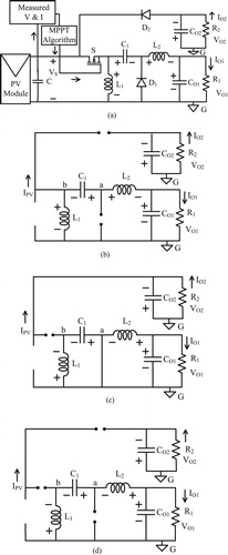
Mode 1: In this mode, the operation is explained for on condition of the switch. Which is displayed in Figure (b). During turn-on time, the supply will pass current through the inductor L1 and it will start charging up to a voltage equal to the supply voltage, VS. The voltage across inductor L2 will also be equal to VS. During this mode of operation, both D1 and D2 diodes are biased in reverse. The operation in mode 2, the switch is made off, and the inductor L1 will release the stored energy with a polarity opposite to the mode 1 operation which is displayed in Figure (c). Inductor L1will release the energy by passing the current through the capacitors CO1& C1 and diodes D1 and D2. The current flows through the inductor L2 through the diode D1 during turn-off. At this time the voltage at point “a” becomes zero. If the voltage drops across the diode D1 is neglected, then the voltage at “a” will be VO1 and the coupling capacitor C1will start charging with a polarity displayed in Figure (c). It implies that the voltage at point “b” will be –VO1. Therefore voltage across L2 will also be –VO1. In this mode, the capacitor CO2 will charge with a lower plate as positive. When inductor, L1 removes all its energy, all devices are turned off and it will enter into mode 3 of operation. So in mode 3 operation, the current does not flow through the L1 inductor. Due to this, the diodes, D1 and D2 will be reverse biased. It is displayed in Figure (d). In Buck-Boost converter because of the reverse biased diodes, the capacitor current will flow through the load from the ground terminal. Therefore the output produced by the buck-boost converter always will have a negative polarity. In Zeta converter the current flow through the load to the ground. Therefore the output produced by the Zeta converter always will have a positive polarity and Buck-Boost converter always will have a negative polarity. Therefore the combination of the Zeta and Buck-Boost will produce a bipolar DC output.
2.2. Solar-fed SEPIC-Cuk combination converter [12]
Both the SEPIC and Cuk converters have the ability of both bucking and boosting of the voltage. This is governed by the duty ratio control. The main advantages of the Cuk converter are that it can provide good characteristics (in terms of filtering on the input and output sides) of both the Buck and Boost converters. Similar to the basic Buck-Boost converter, Cuk converter also produces a negative terminal voltage whereas a SEPIC converter produces a positive polarity output. The energy transfer in the circuit from input to output happens through a coupling capacitor. Here both C1 and C2 are coupling capacitors. The value of coupling capacitors is assumed to be large enough to approximate its voltage to be constant DC in steady-state operation. The circuit diagram of a SEPIC-Cuk combination converter is displayed in Figure (a). Both the inductors L1 and L2 ensure the currents are non-pulsating in the case of Cuk converter whereas; the output currents are pulsating in the case of SEPIC converter. When the switch is made on the diodes D1 and D2 get reverse biased by the large voltage across the coupling capacitors displayed in Figure (b). If the voltage across the diode D2 is neglected, then during turn-on time, the voltage across the coupling capacitor C2 will become VS + VO2. Then the current through the inductor L1 will increase upto a value equal to the supply voltage, VS. At the same time, the condenser, C1 because of its energy stored from the previous cycle also feeds the current to the load and also increases the L2 inductor current.
Figure 2. (a) Circuit diagram of Solar-fed SEPIC-Cuk Combination Converter. (b) Mode 1 operation (during turn ON) of Solar-fed SEPIC-Cuk Combination Converter. (c) Mode 2 operation (during turn OFF) of Solar-fed SEPIC-Cuk Combination Converter.
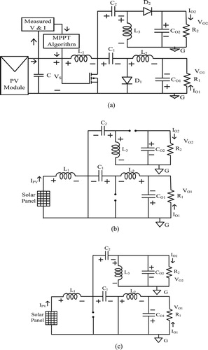
During turn off, the current of the L1 and L2 inductors forces the D1 diode to become conduction. Similarly, the current flowing through the inductor L1 will also force the diode D2 to become forward biased. Here both the inductor currents will flow through the diode D1 in the case of Cuk converter. During this, the current through L1 starts charging the coupling capacitors. And the current through the inductors L2 and L3 will flow through the output capacitor and load and is displayed in Figure (c). In Cuk converter during the turn on and turn off conditions, the current that flows through the load from the ground. Therefore it produces an output with negative polarity. In the case of SEPIC converter, during turn on and turn off conditions, the current is flowing through the load to the ground, therefore, it will produce a positive output voltage across the load.
3. Design of solar fed Zeta-Buck Boost and SEPIC-Cuk Converters
Solar cells are used to convert solar energy into electricity. It is made up of semiconductor materials and which is not required high temperature for the energy conversion. These waves move towards the earth when the sun shines and touches the surface of the solar cells. The various solar cells are connected to form a solar panel. It takes several solar panels to produce sufficient electricity to power a household or high-power application.
3.1. PV cell modelling [1]
A single diode model is used in this document to analyse a solar cell's features under distinct environmental and electrical circumstances. It is displayed in Figure .
Figure 3. Practical single-diode solar cell model.
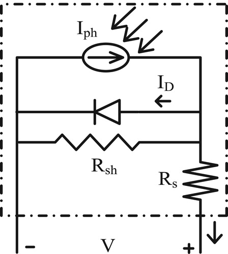
An ideal PV cell contains a sunlight-generated source of current and is called an Iph. Solar irradiance amount has an effect on Iph's value. A P-N diode is a parallel connection to the current source and the final current at the terminal of the circuit displayed as “I”. It is the distinction between the photon current and the current flowing through the diode. V is the terminal voltage of the circuit.
The diode current (ID) is given as,
(1)
(1)
where T = Temperature in K; q = Charge of an electron in coulombs (1.602e-19); k = Boltzmann constant (1.38e-23 J/K); Io = Dark current or Reverse saturation current of the diode at T; VD = Diode voltage in V; n = Ideality factor of the diode (normally between 1 and 2).
The combined resistances of contacts, PN layers and metal grid are termed as series resistance, RS. Leakage current of the PN junction models the shunt resistance, Rsh.
The three demands for solar energy generation are (1) that it should have material capable of absorbing sunlight energy and producing electrons (2) capable of enabling electron movement through the internal circuit and producing the current and (3) that is sufficiently big to generate power. When the incident the energy of sunlight is higher than the energy gap of the material and it will be prepared to release an electron into the conductive band from the valence band. The equations analysing a solar panel is given by,
(2)
(2)
where b = Temperature coefficient; Voc_ref = Reference voltage in the open circuit condition of the solar panel in V.
(3)
(3)
where G, Gr = Measured and reference solar irradiation in W/m2; Isc = Short circuit current in A.
(4)
(4)
(5)
(5)
(6)
(6)
where T, Tr = Measured and reference temperature in K; Rs = Series resistance in ohms; Rsh = Shunt resistance in ohms; Ns, Np = Number of series and parallel solar cells linked; V = Output voltage in V; n = Ideality factor of the diode (normally between 1 and 2).
In this paper, a peak power output capacity of 10 W is analysed. Therefore a PV module capable of producing 10 W with 36 series connected cells is selected. Its open circuit voltage and short circuit currents are 21.6 V and 0.68 A respectively. Theoretically, the highest power will be obtained at 85% of Voc and Isc.
i.e.
Desired output voltage and currents are 24 V and 0.16A respectively.
The designed parameters of the solar panel are mentioned in Appendix 1.
3.2. Design of solar fed Zeta-Buck Boost combination converter [12]
For finding out the maximum switching current, it is necessary to derive an expression for duty ratio. The Zeta converter is a derived Buck-Boost converter topology. Therefore the expression for the duty ratio of normal buck-boost converter holds true for the zeta converter also. So, the same duty ratio expression is valid for the combination converter also.
The expression for the duty ratio (D) of Zeta-Buck-Boost combination converter working in the continuous current conduction Mode can be represented as a function of the output voltage (VO) and the input voltage (VS), and it is given by,
(7)
(7)
The main factor should be considered at the designing of zeta converter is the ripple current (ΔIL) through the inductors L1 and L2.
(8)
(8)
where K = ripple current constant (0.2–0.4)
The expression for the minimum value of inductors L1 and L2 is,
(9)
(9)
The peak current flowing through the inductors L1 and L2 can be defined as a function of duty ratio and the ripple current through it,
(10)
(10)
The minimum value of the output capacitance or the filtering capacitance (CO1) is,
(11)
(11)
= Output ripple voltage (typically 1% of
).
The output capacitor CO2 of the buck-boost converter is required to supply the energy to the load during the time when energy is increasing in the inductor because of the discontinuous nature of the output current. The minimum value of the output capacitor CO2 can be calculated as,
(12)
(12)
where
is the Equivalent Series Resistance of the output capacitor CO2.
The designed parameters of the converter according to the equations explained above are mentioned in Appendix 1.
3.3. Design of solar fed SEPIC-Cuk combination converter [12]
The SEPIC and Cuk converters are also derived Buck-Boost converter topologies. Therefore the expression for the duty ratio of normal Buck-Boost converter holds true for these converters. The duty ratio will help to find out the maximum switching current in a circuit. Therefore the expression for the duty ratio (D) of SEPIC-Cuk combination converter is given as,
(13)
(13)
where Vfwd = forward voltage drop of the Schottky diode.
If the diode voltage drop is neglected, then the Equation (13) can be re-written as,
(14)
(14)
By rearranging the above expression the duty ratio can be represented in terms of the input current (IS) and output current (IO) as,
(15)
(15)
The maximum and minimum duty ratio occurs at a minimum and maximum input voltage. From the Equation (15) it is observed that the duty ratio also can be represented in terms of the input current (IS) and output current (IO).
The ripple current (ΔIL) through the inductor as a function of efficiency (η) can be calculated as,
(16)
(16)
For a desired ripple value of the current, the minimum inductor value of SEPIC converter can be found as,
(17)
(17)
The expression for peak current flowing through these inductors is,
(18)
(18)
The expression for finding the values of the Coupling capacitor C2 and filter capacitor C02 is,
(19)
(19)
where
= Ripple voltage in coupling capacitor C2 (1% of VS)
(20)
(20)
where
= Output ripple voltage (typically 1% of
).
For the Cuk converter, the minimum value of L2 is calculated as,
(21)
(21)
where
is the ripple current through the inductor L2 and it is typically taken as 10–20% of IS.
The maximum current flowing through L2 is,
(22)
(22)
The output capacitor (CO2) can be design identical to that of a normal buck converter and it is given as,
(23)
(23)
where
is the allowed peak to peak ripple in the output voltage of Cuk Converter (VO1)
The coupling capacitor C1 of Cuk converter design is based on limiting the peak-to-peak voltage ripple, and it can be defined as,
(24)
(24)
The design parameters of the converters obtained according to the equations explained above are mentioned in Appendix 1.
4. Control schemes for solar fed converters
In order to get the highest efficiency from the solar panel, it is required to drive the solar panel at its highest power point. The highest power points of any solar panel will change according to the change in the solar irradiation. Therefore, the control scheme which is used to get maximum efficiency from the solar panel is MPPT techniques. The pulses produced by the MPPT, will compare with the switching frequency of the converter and produces corresponding duty ratio to control the switch. The usually used MPPT techniques are P & O, IC, APO etc. among these methods the IC and APO method is discussed in this paper.
4.1. Advanced Perturb and Observe (APO) method [1]
Advanced Perturb and Observation method is an enhanced version of the P & O method. The algorithm starts by measuring the present value of voltage and current and it will calculate the current power. After the power calculation, it will perturb in the direction according to the next tracking of the power point. The flow chart of this algorithm is displayed in Figure (a).
Figure 4. (a) Flow chart of Advanced Perturb and Observation MPPT technique. (b) Flow chart of IC MPPT technique.
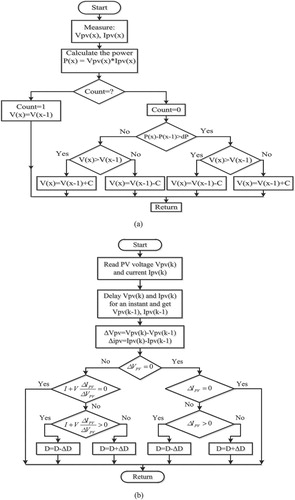
In this method, the number of stages of P & O is increased by (x–1), (x–2) and (x–3). This can increase the tracking velocity of the MPPT controller. The efficiency of the P&O algorithm is therefore enhanced.
4.2. Incremental Conductance (IC) method [1]
There are lot of drawbacks for the P and O algorithm. The IC MPPT technique will overcomes these drawbacks and tracks the power efficiently. In this scheme, the highest power from the panel is extracted by comparing the incremental conductance to the present conductance values. i.e.
(25)
(25)
where
= Instantaneous conductance;
= Incremental conductance.
The IC MPPT technique will be stable at its highest power point and it will change only when the insolation changes are occurred. Here at every time, it will calculate the ratio of power to voltage. Whenever the value of this ratio becomes equal to zero, it indicates that the highest power point is reached. After that, it will be stable at that point till next change in the solar irradiation. According to the rule of derivatives, the power relation can be written as,
Since at MPP, therefore by rearranging the equation,
The highest power point is obtained when this incremental conductance becomes equal to the negative of the instantaneous conductance.
(26)
(26)
The flow chart of this algorithm is displayed in Figure (b).
If , it means that the PV voltage is less than the MPP. In this case, the duty cycle should be increased. If
then the PV voltage is equal to the MPP and if
it means that the PV voltage is greater than the MPP so duty cycle should be decreased.
Both the APO and IC MPPT algorithms will find the actual highest power from the solar panel. Comparatively IC method gives more accuracy than the APO method. That is, when the atmospheric conditions fixed or varying with slow rate, the APO control will oscillates at the highest power point but the IC MPPT gives the suitable quantity at varying nature of atmosphere.
5. Simulation work
MATLAB software is used to simulate the suggested converter. A discrete mode of operation with a 10 µs sampling time is kept. The converter's switching frequency is set to 5 kHz. The solar module is designed for normal test circumstances like 1000 W/m2 and 25°C. It is also tested for varying irradiation. The static performance of the converter is analysed. The converters are operated under Advanced P & O MPPT and IC MPPT control schemes and the results are also compared. From these MPPT techniques, it is observed that the IC method is more efficient than that of Advanced P & O method.
5.1. Performance analysis of Advanced Perturb and Observation (APO) and Incremental Conductance (IC) MPPT technique
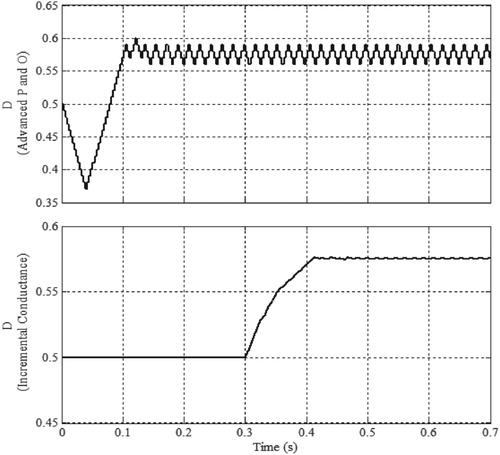
Figure illustrates the comparison between Advanced P & O and IC MPPT Techniques. The waveforms displayed in the figure is Duty ratio, D. from the design, it is found that the highest and lowest values of the duty ratio are 0.6 and 0.55, respectively. And the duty ratio corresponds to the highest power is 0.57. From the figure given below, it is clear that the APO algorithm helps to reach the highest power point faster than the IC algorithm. The APO algorithm takes nearly 0.1s to reach the highest power point whereas the IC algorithm takes 0.3 s. In APO method the duty ratio varying in the range of actual duty ratio value and it is not able to attain stability at actual duty ratio. Therefore by implementing the APO MPPT technique, it will always oscillate nearer to the highest power point. Therefore the efficiency will be lesser than the IC method. In the IC method, it takes more time to reach the actual duty ratio comparing to APO. But after reaching the actual duty ratio it holds for the entire operation. Therefore the efficiency will become higher than that of APO. But implementation of IC MPPT is costlier than APO MPPT. Because in IC MPPT two sensors are required, one for voltage and another for current, whereas in APO only voltage is sensing.
Figure 5. Performance analysis of Advanced Perturb and Observation (APO) and Incremental Conductance (IC) MPPTs.
5.2. Performance of solar-fed Zeta-Buck Boost and SEPIC-Cuk combination converter under Advanced Perturb and Observe MPPT technique
Figure (a) illustrates the performance analysis of Zeta-Buck Boost and SEPIC-Cuk converters under Advanced P and O MPPT technique. The waveforms displayed in Figures are Duty ratio (D), supply or voltage obtained from the PV panel (VPV), panel current (IPV), output voltage, current and power of first converter (VO1, IO1 and PO1), output voltage, current and power of second converter (VO2, IO2 and PO2). From the performance, it is observed that the photovoltaic system has non-linearly varying voltage. The input current (IPV) of the Zeta-Buck Boost converter is discontinuous and of SEPIC-Cuk converter is continuous which is displayed in Figure (a,b). The gate pulse for the switch is generated by the APO MPPT technique. The APO algorithm is executed by measuring the VPV from the solar panel. In Zeta-Buck Boost converter, Zeta has an inductor series to the output preventing the sudden change of the output current that would otherwise increase the ripple terminal voltage. The duty ratio is oscillating at the highest power point.
Figure 6. (a) Performance analysis of Solar-fed Zeta-Buck Boost Combination Converter under Advanced Perturb and Observation (APO) MPPT technique. (b) Performance analysis of Solar-fed SEPIC-Cuk Combination Converter under Advanced Perturb and Observation (APO) MPPT technique
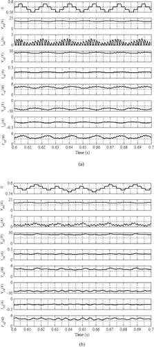
In Zeta-Buck Boost converter, they generate DC bipolar voltages of 25.23 and −25.85 V. The total output power obtained from the converter will be the sum of the output power of Zeta (PO1) and Buck-Boost (PO2) converters. It is obtained as 8.043 W and efficiency of the Zeta-Buck Boost converter is obtained as 79.97%.
Similarly, in SEPIC-Cuk converter, they generate DC bipolar voltages of 24.36 and −23.45 V. The total output power obtained is 7.61 W and the efficiency becomes 76.06%.
5.3. Performance analysis of solar-fed Zeta-Buck Boost and SEPIC-Cuk combination converter under Incremental Conductance (IC) MPPT technique
The performance analysis of Zeta-Buck Boost and SEPIC-Cuk converters controlled by the Incremental Conductance (IC) MPPT technique is given in Figure (a,b). The waveforms displayed in Figures are Duty ratio (D), supply or voltage obtained from the PV panel (VPV), panel current (IPV), output voltage, current and power of first converter (VO1, IO1 and PO1), output voltage, current and power of second converter (VO2, IO2 and PO2). From the performance, it is observed that the photovoltaic system has non-linearly varying voltage. The input current (IPV) of the Zeta-Buck Boost converter is discontinuous and of SEPIC-Cuk converter is continuous which is displayed in Figure (a,b). The gate pulse for the switch is generated by the IC MPPT technique. The IC algorithm is executed by measuring the VPV and IPV from the solar panel. By comparing the IC and APO control techniques, it is observed that IC gives a stable duty ratio which is able to extract highest power from the panel. Moreover, the APO oscillating at the peak power point throughout the operation. It can be observed from the D waveform in Figures and . Therefore, the IC MPPT gives more accurate values than APO MPPT and efficiency is also improved.
Figure 7. (a) Performance analysis of Solar-fed Zeta-Buck Boost Combination Converter under Incremental Conductance (IC) MPPT technique. (b) Performance analysis of Solar-fed Zeta-Buck Boost Combination Converter under Incremental Conductance (IC) MPPT technique
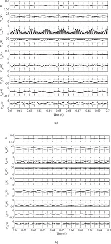
In Zeta-Buck Boost converter, they generate DC bipolar voltages of 25.21 and −25.05 V. The total output power obtained from the converter will be the sum of the output power of Zeta (PO1) and Buck-Boost (PO2) converters which is obtained as 8.596 W. And the efficiency of the Zeta-Buck Boost converter is obtained as 85.47%. Similarly in SEPIC-Cuk converter; they generate DC bipolar voltages of 25.52 and −24.74 V. The total output power obtained is 8.4205 W and the efficiency becomes 83.29%. The improvement in the efficiencies while implementing IC over APO MPPT method is, 5.5% in the case of Zeta-Buck Boost and 7.2% in the case of SEPIC-Cuk converters. The comparative analysis of both the converters under both the MPPT techniques is shown in Table .
Table 1. Performance of solar fed Zeta-Buck Boost and SEPIC-Cuk combination converters at 1000 W/m2 solar irradiation.
5.4. Dynamic performance of Zeta-Buck Boost and SEPIC-Cuk converter under varying solar irradiation
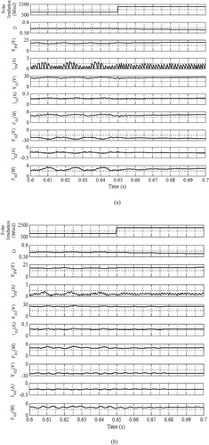
From the above analysis, it is observed that converters with Incremental Conductance (IC) MPPT algorithm has higher efficiency than that of Advanced Perturb and Observation (APO) MPPT algorithm. Therefore the varying solar irradiation is applied only for Zeta-Buck Boost and SEPIC-Cuk converters with IC MPPT and it is displayed in Figure (a,b). While varying the solar irradiation from 1000 to 2000 W/m2, the output voltage from the PV panel is increased. This increased the converter output also. It means that, while increasing the radiation, the panel will be able to operate at its maximum designed power level. So the power taken by the converter input side will be increase and effectively the converted power at output side will also increase as shown in Figure (a,b). For this, the simulation model is run at 1000 W/m2 irradiation till 0.65 s. Again, level of Irradiation is increased to 2000 from 0.65 till 0.7 s at end of simulation performance. From this dynamic performance, it is observed that system is working satisfactory even this large variation.
Figure 8. (a) Performance of Zeta-Buck Boost converter with IC MPPT under varying solar irradiation from 1000 to 2000 W/m2. (b) Performance of SEPIC-Cuk converter with IC MPPT under varying solar irradiation from 1000 to 2000 W/m2.
6. Test results
The solar fed Zeta-Buck Boost and SEPIC-Cuk converters for small power application are implemented. The Incremental Conductance (IC) MPPT algorithm is programmed using OP-5142 based real-time simulator. OP-5142 allows the integration of the FPGA technologies in the simulator for implementation of HDL functions and high speed and high-density digital inputs/ outputs in real-time models. It allows the connectivity of 4 digital and/ or analog output modules. It provides high precision switching with a maximum capacity of 100 MHz. The maximum output voltage of analog channel is 16 volt. The performance waveforms have been captured with Digital Storage Oscilloscope (DSO). The switching frequency of the converter is chosen as 5 kHz throughout the implementation. The performance waveforms are displayed in Figures and with the discussion.
Figure 9. (a–c) Hardware performance analysis of Zeta-Buck Boost converter under Incremental Conductance MPPT. (a) In y-axis: CH1-500 mV/div, CH2-10 V/div, CH3-1A/div; In x-axis:500 µs/div, (b) In y-axis: CH1-10 V/div, CH2-500 mA/div, CH3-5 V/div; In x-axis:5 ms/div, (c) In y-axis: CH1-10 V/div, CH2-500 mA/div, CH3-5 V/div; In x-axis:5 ms/div.
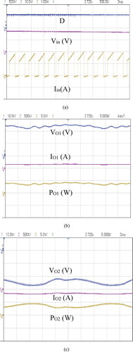
Figure 10. (a–c) Hardware performance analysis of SEPIC-Cuk converter under Incremental Conductance MPPT. (a) In y-axis: CH1-500 mV/div, CH2-10 V/div, and CH3-1A/div; In x-axis:10 ms/div, (b) In y-axis: CH1-10 V/div, CH2-500 mA/div, and CH3-5 V/div; In x-axis:10 ms/div, (c) In y-axis: CH1-10 V/div, CH2-500 mA/div, and CH3-5 V/div; In x-axis:10 ms/div.
6.1. Performance of solar-fed Zeta-Buck Boost converter with Incremental Conductance MPPT
The performance analysis of implemented Zeta-Buck Boost converter is displayed in Figure . Figure (a) shows Duty ratio (D), the Input voltage (Vin) and input current (Iin). The duty ratio equivalent to the highest power is obtained at 0.57. From this test setup, the solar panel is capable of working at highest power point and the voltage corresponding to the highest power point is 17 V. The nature of input current drawn by the Zeta-Buck Boost converter is discontinuous and it is displayed in CH3 of Figure (a). The hardware is tested for constant solar irradiation of 1000 W/m2 and a temperature of 25°C.
The outputs obtained from Zeta-Buck Boost converter is separately displayed in Figure (b,c). Figure (b) gives the output of Zeta converter and Figure (c) shows the outputs of the Buck-Boost converter. VO1, IO1 and PO1 represent the voltage, current and power obtained from the Zeta converter and VO2, IO2 and PO2 represents the voltage, current and power obtained from the Buck-Boost converter. In both the waveforms, the CH1, CH2 and CH3 denotes the output voltage (VO1 and VO2), output current (IO1 and IO2) and output power (PO1 and PO2). The VO1 and VO2 of the Zeta and Buck-Boost converters are DC bipolar of value 25 V. The total power delivered from the converter is 8.5965 W. The total losses in this converter are less compared to the APO implemented Zeta-Buck Boost converter. Therefore efficiency is improved by 5%.
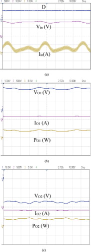
6.2. Performance of solar-fed SEPIC-Cuk converter with IC MPPT
The performance analysis of implemented SEPIC-Cuk converter is displayed in Figure . Figure (a) shows Duty ratio (D), the Input voltage (Vin) and input current (Iin). The duty ratio equivalent to the highest power is obtained at 0.57. The solar panel is able to deliver the highest power throughout the operation and the available maximum voltage is 17 V. The input current waveform of the SEPIC-Cuk converter is continuous in nature and it is displayed in Figure (a) in CH3. The hardware is tested for constant solar irradiation of 1000 W/m2 and a temperature of 25°C.
The outputs obtained from SEPIC-Cuk converter are separately displayed in Figure (b,c). Figure (b) gives the output of the SEPIC converter and Figure (c) shows the outputs of the Cuk converter. VO1, IO1 and PO1 represent the voltage, current and power obtained from the SEPIC converter and VO2, IO2 and PO2 represents the voltage, current and power obtained from the Cuk converter. In both the waveforms CH1, CH2 and CH3 denotes the output voltage (VO1 and VO2), output current (IO1 and IO2) and output power (PO1 and PO2). The VO1 and VO2 of the SEPIC and Cuk converters are DC bipolar of values of 25 and −24.7 V. And the total power delivered from the converter is 8.42 W. The total losses in this converter are less compared to the APO implemented SEPIC-Cuk converter. Therefore efficiency is improved 7% more. The results obtained from the hardware implementation of both Zeta-Buck Boost and SEPIC-Cuk combination converter is shown in Table .
Table 2. Performance of solar Fedzeta-Buck Boost and SEPIC-Cuk converters at 1000 W/m2 solar irradiation.
7. Conclusion
The single-input and two-output converter implemented with Incremental Conductance (IC) MPPT has more efficiency than that implemented with Advanced Perturb and Observation (APO) method. The IC MPPT algorithm always gives a stable duty ratio corresponds to the highest power whereas APO algorithm is varying in nature. Moreover, the time taken for reaching the highest power point is more in IC compared to the APO method. An improvement in efficiency of 5% and 7% is achieved in the proposed Zeta-Buck Boost and SEPIC-Cuk combination converter while implementing with IC MPPT. The solar panel produces exact characteristics curves given in the datasheet. One of the disadvantages found out while designing the converters is that the setup will become bulkier due to more number of the components. To lower the spark on the switch, the switch terminals are connected to ground during the implementation. These converters are useful in the field of battery charging, 24 V power supplies, telecommunications, microelectronics, electric vehicles and other small power level applications.
Disclosure statement
Authors do have any conflict of interest.
References
- Solanki Chetan S. Solar photovoltaics: fundamentals, technologies and applications. New Delhi: PHI Learning Pvt.; 2015.
- Tariq M, Bharadwaj S, Rashid M. Effective battery charging system by solar energy using C programming and microcontroller. Am J Electr Power Energy Syst. 2013;2(2):41–43. doi: 10.11648/j.epes.20130202.12
- Nikolova S, Causevski A, Al-Salaymeh A. Optimal operation of conventional power plants in power system with integrated renewable energy sources. J Energy Convers Manag. 2002;65:697–703. doi: 10.1016/j.enconman.2011.11.035
- Alawekar PP, Bombale UL, Shinde NN. MPPT based charge controller for off-grid small wind machine using PWM technique. Int J Comput Appl. 2013;81(9):22–25.
- Siva ChenthilRajan SM. A new method for rapid maximum power point tracking of PMSG wind generator using PI fuzzy logic. Int J Eng Trends Technol. 2016;36(2):76–81. doi: 10.14445/22315381/IJETT-V36P214
- Bellia H, Youcef R, Fatima M. A detailed modelling of photovoltaic module using MATLAB. NRIAG J Astron and Geophys. 2014;3:53–61. doi: 10.1016/j.nrjag.2014.04.001
- Nguyen XH, Nguyen MP. Mathematical modelling of photovoltaic cell/module/arrays with tags in Matlab/ Simulink. Nguyen Nguyen Environ Syst Res. 2015;4(24):234–239.
- Rakib Hasan M, Sabbir Hossain M, Rahman KP. Design and construction of a portable charger by using solar cap. Glob J Res Eng. Mech Mech Eng. 2017;17(5):14–18.
- Ferrera Prieto MB, Litran SP, Aranda ED, et al. New single-input multiple-output converter topologies: combining single switch non-isolated DC-DC converters for single-input, multiple output applications. IEEE Ind Electron Mag. 2016;10(2):6–20. doi: 10.1109/MIE.2016.2550000
- Xing Y, Ma EWM, Tsui KL, et al. Battery management systems in electric and hybrid vehicles. Energies. 2011;4(11):1840–1857. doi: 10.3390/en4111840
- Napoles J, Leon JI, Franquelo LG, et al. Selective harmonic mitigation technique for multilevel cascaded H-bridge converters. 35th Annual Conference of IEEE Industrial Electronics, Porto, Portugal; 2009. p. 806–811 .
- Mohan N, Undeland TM, Robbins WP. Power electronics: converters, applications, and design. New York (NY): John Wiley & Sons Inc; 1995.
- Rashid MH. Power electronics: circuits, devices and applications. New York (NY): Pearson Education Asia; 2009.
- Williams BW. Generation and analysis of canonical switching cell dc-to-dc converters. IEEE Trans Ind Electron. 2013;61:329–346. doi: 10.1109/TIE.2013.2240633
- Tse KK, Chung HS, Hui SYR, et al. Spectral characteristics of randomly switched PWM DC/DC converters operating in discontinuous conduction mode. IEEE Trans Ind Electron. 2000;47:759–769. doi: 10.1109/41.857956
- Williams BW. Unified synthesis of tapped-inductor DC-DC converters. IEEE Trans Power Electron. 2014;29(10):5370–5383. doi: 10.1109/TPEL.2013.2291561
- Grant DA, Darroman Y, Sutter J. Synthesis of tapped-inductor switched mode converters. IEEE Trans Power Electron. 2007;22(5):1964–1969. doi: 10.1109/TPEL.2007.904215
- Oropeza F, Lorea L, Macias-Diaz Aa. Two inductor boost converter start-up and steady-state operation. Braz J Power Electron. 2010;15:143–149.
- Chen J, Maksimovic D, Erickson R. Buck-boost PWM converters having two independently controlled switches. Proceedings of IEEE 32nd Annual Power Electronics Specialists Conference, Vancouver, BC, Canada, Vol. 2; 2001 . p. 736–741.
- Patra P, Patra A, Misra N. A single-inductor multiple-output switcher with a simultaneous buck, boost and inverted outputs. IEEE Trans Power Electron. 2012;27(4):1936–1951. doi: 10.1109/TPEL.2011.2169813
- Chakraborty S, Jain AK, Mohan N. A novel converter topology for multiple individually regulated outputs. IEEE Trans Power Electron. 2006;21(2):361–369. doi: 10.1109/TPEL.2005.869741
- Nami A, Zare F, Ghosh A, et al. Multi-output DC-DC converters based on diode-clamped converters configuration topology and control strategy. IET Power Electron. 2009;3(2):197–208. doi: 10.1049/iet-pel.2008.0341
- Mishra SK, Nayak KK. Boost topology based multi-output converters. IEEE Trans Ind Electron. 2005;5(19):76–83.
- Boora AA, Zare F, Ghosh A. Multi-output buck-boost converter with enhanced dynamic response to load and input voltage changes. IET Power Electron. 2011;4(2):194–208. doi: 10.1049/iet-pel.2009.0269
- Onwuchekwa CN, Kwasinski A. A modified-time-sharing switching technique for multiple-input DC-DC converters. IEEE Trans Power Electron. 2012;27(11):4492–4502. doi: 10.1109/TPEL.2011.2180740
- Gavriş M, Cornea O, Muntean N. Multiple input DC-DC topologies in renewable energy systems – a general review. Proceedings of 3rd IEEE International Symposium on Exploitation of Renewable Energy Sources, Subotica, Serbia, Vol. 6; 2011 .p. 123–128.
- Yalamanchili KP, Ferdowsi M. Review of multiple input DC-DC converters for electric and hybrid vehicles. IEEE Trans Power Electron. 2005;10(25):552–555.
- Dahalea S, Aakriti Dasb N, Pindoriya M, et al. An overview of DC-DC converter topologies and controls in dc micro-grid. Proceedings of 7th International Conference on Power Systems (ICPS), Pune, India, Vol. 13; 2017 . p. 410 −415.
- Xi Y, Jain P, Liu Y-F. A precisely regulated multiple output forward converter topology. Proceedings of IEEE Applied Power Electronics Conference, New Orleans, LA, USA, Vol. 2, No. 8, June 2000 .p. 986–992.
Appendix 1
A.1 System parameters for simulation of solar panel
The electrical requirements are subject to normal testing circumstances of 1000 W/m2 and a panel temperature of 250C.
A.2 System parameters for Zeta-Buck Boost combination converter
PV voltage of 17 V and current of 0.58A, Linear load with R1, R2 = 150 Ω, L1, L2 = 5.208 mH, ESR of L1, L2 = 83 mΩ, C1 = 208.3 µF, ESR of C1 = 5 mΩ, CO1, CO2 = 21.69 µF, ESR of CO1, CO2 = 5 mΩ, on resistance of MOSFET is 1.2 mΩ, internal diode resistance of MOSFET is 0.01 Ω, switching frequency (fs) = 5 kHz.
A.3. System parameters for SEPIC-Cuk combination converter
PV voltage of 17 V and current of 0.58A, Linear load with R1, R2 = 150 Ω, L1, L2, L3 = 4.309 mH, ESR of L1, L2, L3 = 83 mΩ, C1, C2 = 315 µF, CO1, CO2 = 210 uF, ESR of C1, C2, CO1, CO2 = 5 mΩ, on resistance of MOSFET is 1.2 mΩ, internal diode resistance of MOSFET is 0.01 Ω, switching frequency (fs) = 5 kHz.