
 ?Mathematical formulae have been encoded as MathML and are displayed in this HTML version using MathJax in order to improve their display. Uncheck the box to turn MathJax off. This feature requires Javascript. Click on a formula to zoom.
Abstract
This paper focuses on experimented space projects run by universities, offering an effective design process to improve learning methods in space engineering. The approach used for the design of CubeSat Electrical Power System (EPS) will go through estimations, sizing, simulations, PCB design and end with an experimental test procedure for design validation. The main design criteria presented in this paper are low costs and effective reliability. To meet the first criterion, the Commercial-Off-The-Shelf (COTS) components are used during the design, which has become an effective path to put experimental payloads in orbit for minimal cost. In the second criterion, the function of some critical EPS components was replicated, such as circuits used for power maximization and battery charge regulation, by following a suitable algorithm embedded in MCU and hot/cold redundant analog integrated circuits. However, the choice was made on the state of the art of CubeSat components already tested. This approach of working will help new space engineers to think about optimal solutions for the design of the appropriate EPS for a CubeSat university project achievable on a limited budget. Finally, the necessary experiments of the designed EPS were carried out and the results were illustrated in the context below.
1. Introduction
This last decade has seen a significant development of small and nanosatellites launched and put into orbit. These nanosatellites are mostly designed, built, tested, and operated according to the CubeSat standard, which was developed in 2000 by California Polytechnic State University and Stanford University [Citation1]. A nanosatellite with the dimensions of one, two, up to three cubes that can be built and launched is named, a single CubeSat (denoted 1U), a double CubeSat (denoted 2U), or a triple CubeSat (denoted 3U), respectively. To offer more flexible mission profiles (interplanetary missions, communication, astrochemistry, and astrobiology research with larger payload), a sextuple CubeSat (denoted 6U) up to 12U nanosatellite is nowadays being considered, while preserving the advantages offered by standardization, by varying the profile of the CubeSats deployed into orbits [Citation2,Citation3]. Space agencies, especially NASA, are experimenting with using CubeSats to deal with scientific problems, such as 6U nanosatellites launched in 2018 towards Mars for a telecommunications experiment [Citation4]. CubeSats are placed in their orbits using a closed deployer, such as Poly PicoSatellite Orbital Deployer (PPOD), which can be loaded with three-1U CubeSat, one 2U and one 1U or one 3U nanosatellite. While 6U or 12U nanosatellite are generally designed for deployment from International Space Station (ISS) via NanoRacks [Citation5]. Compared with large-scale satellites projects, CubeSats are low-cost for the launch and the hardware, with a short period of development and fast delivery [Citation6].
Such satellites are more appropriate in universities and have become an operative tool in astronautical sciences, space engineering education, and training. This is a good initiative for new engineers and universities related to space engineering, with the cooperation of different start-up space companies, on the one hand, to design and develop nanosatellite projects that can be adopted by certain developing countries. On the other hand, the successful development of these nanosatellites, technologies, and associated methods would allow for easier access to space, creation or development of inexperienced aerospace sectors, leading to new markets and applications [Citation7,Citation8]. While the developed spaceframe must follow the CubeSat design specifications, as well as meet the customer’s needs [Citation9]. Intelligent manufacturing with shared and efficient transfer of technological advancements will continuously ensure and satisfy the market trends regarding nanosatellites components [Citation10]. It should be noted that the active pursuit and development of small launchers is one of the reasons for the reduction in launch costs and the opportunities for nanosatellite flights. Many initiatives and the first successful result took place in January 2018: on its second flight, Rocket Lab's Electron rocket reached orbit and deployed three CubeSats [Citation11,Citation12].
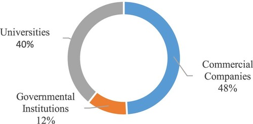
For countries with emerging technology sectors, nanosatellites can raise private business development with reasonably small capital investments, or offer growth markets for remaining companies. Moreover, in these countries, a nanosatellite development programme at university is an ideal first step to establish such a basic capacity. Experience gained through on-the-job training, working through the complete project phases from designing, assembling, and testing a satellite, is decisive to gain this industrial space capacity [Citation13–16]. For developed countries, nanosatellite projects are focusing on learning methodology and training students; to do similar work to that established in different companies and space agencies. In the preliminary phases of a satellite project, experts in each of the space areas come from, for example, the ESA Concurrent Design Facilities (CDF), CNES, Airbus Defense and Space, to supervise students at a limited time for the development of a feasibility phase of space missions [Citation17–19]. According to the statistics presented in Figure , in 2019, about 438 nanosatellites were launched, of which commercial companies and universities have launched a significant number of nanosatellites compared to governmental institutions [Citation20].
Figure 1. Categories of launched nanosatellites.
Some objectives of University Nanosatellite Projects were identified incrementally:
Teaching students and future space engineers with theoretical as well as efficient hands-on experience in satellites design and manufacturing,
Real experience in satellite control and payload operations,
Low-cost space applications,
Testing and understanding first-hand designs, technologies, and prototypes,
Validation and test of new components,
Obtain comprehensive housekeeping data for subsystem evaluation [Citation21],
Implication of radio amateur society for receiving beacons from nanosatellites.
The increased launch of nanosatellites is due to the rapid advances in miniature technologies, which have made several low-cost Commercial-Off-The-Shelf (COTS) subsystems and components available in areas such as telecommunications, data handling, and acquisition, power electronics, and instrumentation. The subsystems and components selection criteria also take into consideration the space environment tests results and heritage of earlier space missions, while maintaining subsystems’ low-cost [Citation22,Citation23]. Therefore, in nanosatellites projects, components’ selection is based on low-cost COTS technology with considering the volume constraints and the limitations of the budget. Generally, the nanosatellite subsystems are considered to be assembled by publicly available COTS components in many markets and using fast manufacturing services to reduce the duration of the project (such as CNC machines and 3D printers) [Citation24].
One of the crucial parts of any satellite mission is the Electrical Power System (EPS), which is responsible for power conversion from solar panels, energy storage in batteries, and power distribution to other subsystems. Therefore, together with the system backplane, an EPS prototype designed for the nanosatellite project has the following principal functions:
Power source regulation,
Power storage,
Power distribution.
Telemetry measurements and conditioning,
Control of antenna’s deployment system,
Over-current protection.
In the literature, some universal surveys on Nanosatellites/CubeSats have focused on mission characteristics, implemented technologies and overall success rates [Citation2,Citation3]. However, design methods and testing processes have rather been discussed to be useful for CubeSat university projects only. Therefore, the main contribution of this paper is to present suitable EPS design (components sizing and selection) and test procedures. The reliable PPT circuit is used based on the Maximum Power Point Tracking (MPPT) algorithm combined with Battery Charge Regulation (BCR) method, which is implemented in MicroController Unit (MCU) and a redundant analogue circuit. While, in case of MCU failure, the redundant MPPT and BCR, which is available in analogue Integrated Circuit (IC), is used for power optimization, charge regulator, and overvoltage protection of the battery.
Some requirements that should be considered for the EPS design are:
EPS power capability shall cover the mission power budget in nominal cases, during an eclipse and high-power consumption periods,
Lasts during the mission lifetime,
Reliability and robustness against harsh space environment.
Figure 2. Design process for EPS of CubeSat.
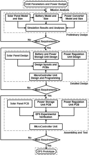
Based on the above flowchart, the remainder of this paper is structured as follows:
In section 2, a mission analysis including the power budget of the proposed CubeSat is presented. For the preliminary design of this engineering prototype, the power consumption of the subsystems is estimated from the associated design reports and datasheets, which will be then used for sizing the EPS parts. Section 3 is dedicated to the proposed EPS components (solar panel, power regulator, battery, power storage, and microcontroller) configuration design for CubeSat. Then, in section 4, the preliminary and the detailed design based on simulations are presented to check the sizing parameters and components selection of each EPS unit. The experimental verification of the designed EPS units is presented in section 5. The power production calculations from the proposed solar generator, used in the preliminary design previously presented, can be iteratively corrected and tuned, based on the experimental testing of the proposed assembled PV panel. In section 6, the cost of each EPS component is evaluated. The conclusion and outcomes of this work are discussed in the last section.
2. Mission analysis and power budget
The studied nanosatellite is 1U CubeSat that has dimensions of 10cm of width, 10cm of length, and 10cm of height. The mass is not exceeding 1.33Kg. The CubeSat surface is covered with solar cells and different surface coatings. The structure of 1U CubeSat is shown in Figure . The main mission of this CubeSat is to test a camera for astronomical observation such as stars and phenomena in space (airglow).
Figure 3. 1U CubeSat structure [Citation27].
![Figure 3. 1U CubeSat structure [Citation27].](/cms/asset/1098b63c-9a0d-4906-98a9-d99478ecd681/taut_a_2065420_f0003_oc.jpg)
The chosen mission orbit is a Sun Synchronous Orbit (SSO) with an altitude of 500km and an LTDN of 10.30 AM. The orbit parameters are shown in Table , which are obtained by calculations from the developed model based on the literature [Citation12]. As an additional feature, those parameters have been compared with System Tool Kit (STK) results obtained in the numerical simulations. For the nanosatellite visibility analysis, the ground station is supposed to be located at Beihang University (39.9824° N, 116.3488° E). On the one hand, if there is a problem at the main ground station (Beihang University) that makes it unable to operate, backup ground stations can be used from which radio contact can be maintained. For the continuity of operations plan, commands can also be authorized from these redundant ground stations. On the other hand, other stations in the amateur radio community may be allowed to listen to, download, and decode CubeSat data. For this purpose, the frequencies and operating modes of this CubeSat can be published.
Table 1. Mission parameters.
The EPS is designed to meet the mission requirements, survive during the mission lifetime, and to supply the subsystems that have been defined as:
On-Board Data Handling (OBDH),
Communication system (Transceiver (Tx) and Receiver (Rx)),
Attitude Determination & Control System (ADCS),
Payload (low power camera for a test).
Table 2. Power consumption of subsystems.
The power consumed by the EPS represents the losses when supplying the subsystems and charging the battery. In this study, there are also three different mission power modes (see Table ), defined as follows:
Table 3. Power of different mission modes.
Common mode: the CubeSat is in orbit with no operational payload and communication; sleep OBDH, and low power consumption by ADCS. Therefore, in this mode, for the power budget calculation, OBDH is activated with minimum power consumption, ADCS is activated with minimum power consumption. The EPS is supposed to consume, at the minimum and the maximum in each common mode, respectively 300mW during eclipse period and 400mW during sunlight period.
Mission mode: the CubeSat fulfils its missions by exploiting its payload with the full activation of OBDH and the function of ADCS. Then in this mode, for the power budget calculation, OBDH is activated with maximum power consumption. While the camera is processing, ADCS is activated with minimal power consumption, and the CubeSat is in mission mode with minimal power. Whereas the ADCS is at its maximum power consumption when pointing the camera for image acquisition at the target, and the CubeSat is in mission mode with maximal power. The EPS is supposed to consume, at the minimum and the maximum in each mission mode, respectively 300mW during eclipse period and 400mW during sunlight period.
Communication mode: mission and telemetry data are sent to the ground station and remote commands are received from the ground station. Therefore, in this mode, for the calculation of the power budget, OBDH is activated with maximum power consumption. While ADCS is activated with minimum power consumption when receiving commands from the ground station and maximum power consumption when the CubeSat is pointed towards the ground station to downlink data. The EPS is supposed to consume, at the minimum and the maximum in each communication mode, respectively 300mW during eclipse period and 400mW during sunlight period.
The above mission power modes can be changed even their power consumption (see Table ). The decision of which system is activated, how will work (maximum or minimum) and its activation period is subject to many changes depending on the concept of operations and mission plan. However, in the design stage for the initial start-up, a rough definition of a preliminary mission analysis is necessary to establish the design and sizing of the EPS. Accordingly, after many iterations, the worst-case power consumption will be considered for the rest of the design and sizing calculation.
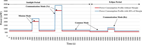
According to ECSS standards and SMAD, a margin from 5% up to 20% or 25% has to be applied to meet the mission power budget used for sizing depending on the level of the design maturity [Citation28,Citation29]. Based on the different power consumption modes of the CubeSat, Figure shows, during one orbit, the simulated baseline scenario of the power consumption profile with both 20% of the margin and without margin. In this simulation, the mission mode and the two different communication modes (Tx and Rx) are taken into account, which means a worst-case orbit scenario.
Figure 4. Mission power consumption profile, baseline scenario (worst-case).
The total energy required, during one orbit, from both solar panel and battery power sources is expressed in the following equation:
(1)
(1) Where Eday,need is the energy needed during the daylight period, Eecl,need is the energy needed during the eclipse period. Pi, i = 1, 2, … .n, gives the typical power profile for subsystems and payload operation during one orbit. The efficiency factors are
(from PV panels to loads) and
(from batteries to loads). According to the literature [Citation30] and with the consideration of a PPT circuit,
and
can be chosen. However, due to the fact that the losses of the various power converters have already been considered for power budget and that a margin of 20% will also be taken into account for the sizing, these coefficients are assumed to be equal to 1.
3. Proposed EPS configuration design
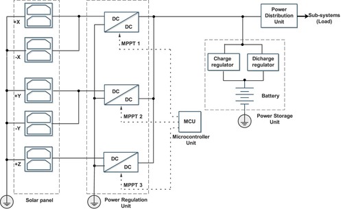
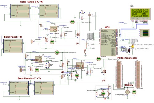
The EPS configuration is shown in Figure .
Figure 5. Proposed EPS configuration for CubeSat with open solar panels structure.
3.1. Hardware design
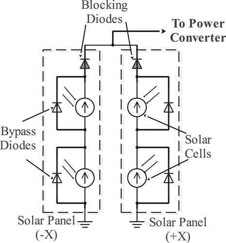
The CubeSat solar cells are mounted on five of the six facets, every two solar panels from opposite sides are connected to one boost converter leading to three DC-DC power converters in total (see Figure ). This proposed configuration presents a good compromise in the use of converters, compared to the use of one converter for each solar panel. In this configuration, only one solar panel per pair can be straight illuminated by the sun at any given time and will be the main power source. The second solar panel provides a small amount of power due to albedo illumination from the Earth. A similar topology is used in commercial CubeSat EPS from ClydeSpace, as presented in [Citation31].
In the above topology (Figure ), the configuration ensuring system reliability is adopted when: the loss of a single DC-DC boost converter or damage to a solar panel does not disable the entire EPS, where the defective part is electrically separated. This fault isolation is guaranteed by the use of bypass diodes and blocking diodes [Citation32]. There is no requirement to regulate the main bus, as the subsystems themselves will separately regulate their specific supply from their decentralized power distribution unit [Citation33,Citation34].
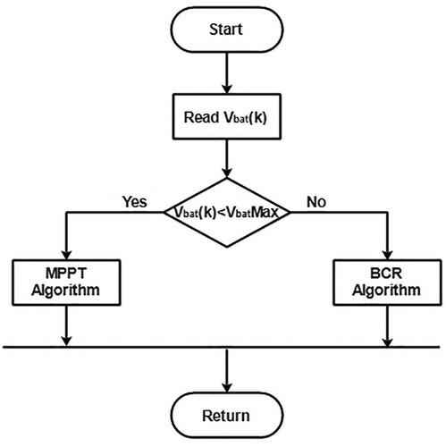
3.2. Software design
The power converters can be connected in parallel, each of them being controlled with its algorithm based on the Maximum Power Point Tracking (MPPT) and Battery Charge Regulator (BCR) implemented in the MicroController Unit (MCU). The proposed MPPT is based on Perturb and Observe (P&O) technique that is widely used for PV application [Citation35,Citation36]. To prevent overcharging and protect the battery, the BCR method is introduced with the MPPT algorithm. The implemented software control strategy is presented in the flowchart shown in Figure .
Figure 6. Flowchart of the implemented control strategy.
4. EPS design and simulation verification
In this section, by the conducted simulation based on the real parameters, the selection and size of the EPS components will be tested.
4.1. Solar panels
For this proposed CubeSat, the triple-junction solar cells based on 3G30A technology InGaP/GaAs/Ge are selected, which are provided by AzurSpace with an integrated bypass diode. The space-qualified solar cells have an efficiency of 29.6% and providing 2.409V of output voltage and 502.9mA of output current when the Maximum Power Point (MPP) is reached [Citation37]. The mathematical model of the solar cell used in this paper can be found in [Citation38–42]. The curves I(V) and P(V) of the AzurSpace solar cell, under the constant irradiance condition of 1367W/m2 and different values of temperature, are shown in Figure .
Figure 7. AzurSpace PV cell characteristics influenced by temperature: Curves of current and power versus voltage.
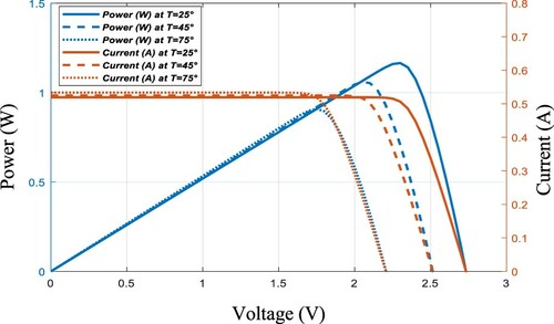
From the characteristics shown in Figure , each cell can produce MPP voltages in the interval of [1.8V-2.3V]. For the proposed application, as shown in Figure , it was decided to use on each PV panel two cells connected in series and then PV panels of two sides connected in parallel for one power converter.
Figure 8. Proposed connection of solar cells for PV panel.
The curves I(V) and P(V) of the solar panel based on AzurSpace cells, under the constant condition of light and different values of temperature, are shown in Figure .
Figure 9. PV panel characteristics based on AzurSpace solar cells influenced by temperature: Curves of current and power versus voltage.
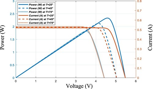
According to the characteristic shown in Figure , based on the series connection configuration (see Figure ), the MPP voltages across the PV panel will be varying in the interval of [3.6V-4.6V].5he rotation around the horizontal plane is defined by variations of angle β. The total generated power by the solar panels whatever the angle β or α (whatever the attitude of the satellite) is shown in Figure .
Figure 10. Generated power as a function of incident light angles: (a) Ideal case;(b) Worst case.
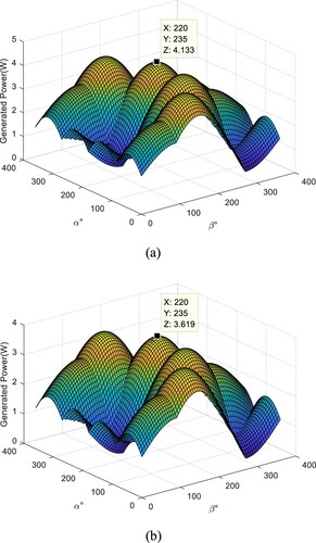
Figure (a) shows the generated power behaviour dependent on the sun incident angles variation in nominal mode. In such conditions, the maximum power that can be generated by the CubeSat is 4.14W, leading to an average value of 2.64W. Whereas, in worst-case conditions (Figure (b)), these values are 3.6W and 2.29W respectively, resulting in a 13% decrease in the available power.
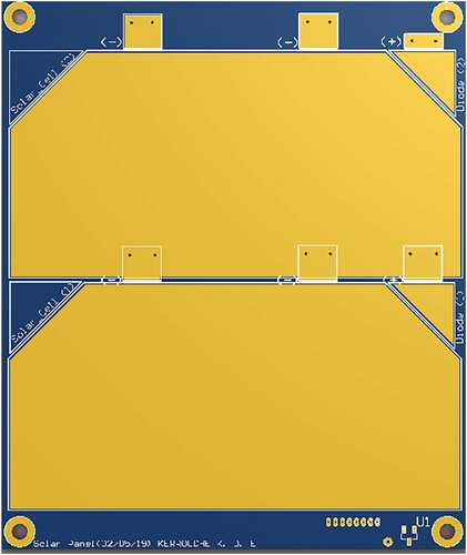
The PCB prototype of the designed solar panel is shown in Figure . This PCB contains two solar cells, as proposed in this study, where they are connected by two bypass diodes. The component U1 is a temperature sensor used for telemetry. The power and telemetry data are connected to the EPS circuit by an eight-pin header. A set of four holes for fastening the solar panel’ PCB to an aluminium panel mounted on CubeSat inner holding structure (see Figure ). The solar panels PCB assembling is presented and well explained in [Citation43].
Figure 11. Solar panel PCB.
4.2. Battery and Power Storage Unit
The power required to charge the battery is calculated as the difference between the generated power to the mission required power in sunlight and eclipse periods (without margin):
(2)
(2)
As a requirement, the accumulated power (Eacc = 1.22Wh) has to be higher than the energy needed during the eclipse (Eecl_needs = 0.39Wh) to overcome any power consumption scenario. Otherwise, for the next orbits, the CubeSat will not have sufficient power and will not be capable to charge the battery as well. The design and technological choice of the battery must take into account many factors (electrical and environmental). The most decisive factor is the capacity of the battery, obtained using the following formula:
(3)
(3) Where Depth of Discharge (DoD) is recommended to be 20% according to the mission lifetime based on existing literature [Citation30]. Then, for the sizing of the battery capacity, a margin of 20% in the total power budget is used, as the EPS is to be developed.
The battery technologies and their characteristics based on Li-Ion chemistries are summarized in Table .
Table 4. Review of the Space commercially available Li-ion cell chemistries and their characteristics [Citation44].
Chin et al. summarized in [Citation44] descriptive COTS battery technologies, as presented in Table , according to their maximum discharge rate capability and nominal capacity. In [Citation45], performances of CubeSat battery technologies, expected in the LEO application, have been tested and compared. When using a Li-Ion battery based on the nanophosphate technology, it is important to take into account the actual orbit conditions. It has been noticed, for Lithium Iron Phosphate (LiFePO4), that the degradation rate, especially at lower temperatures, is much less than the other technologies and it outperforms them.
In this project, the choice was focused on A123 Systems’ LiFePO4 rechargeable APR18650M1A cell [Citation46], which has the highest discharge rate capability, excellent safety, long storage life, and has greater exploitation tolerance due to the use of this technology [Citation47,Citation48]. For LiFePO4 technology [Citation46,Citation49], the apparent voltage and capacity of the battery were found to be less than its total capacity at −20°C compared to that at 25°C. As a result, in this proposed design, the total battery capacity must be doubled; this will balance the capacity reduction of up to 50% when considering the temperature decrease. The accumulators’ selection is based on charge and discharge conducted tests aimed to choose two accumulators that have identical electric performance, as adopted in [Citation50].
Figure illustrates the discharge characteristics of Lithium- Iron Phosphate (LiFePO4) APR18650M1A battery, where, these characteristics can be distinguished into three zones. First, the exponential zone represents the battery voltage overshoot above the rated value. Then, after the no-load mode, the operating point of the battery is in the nominal zone for a period of establishing a fixed discharge current value, where the voltage is changed slightly. Finally, when the nominal capacity of the battery is reached, it is followed by the third operating zone, where the battery voltage decreases rapidly.
Figure 12. Discharge characteristics of rechargeable LiFePO4 APR18650M1A battery.
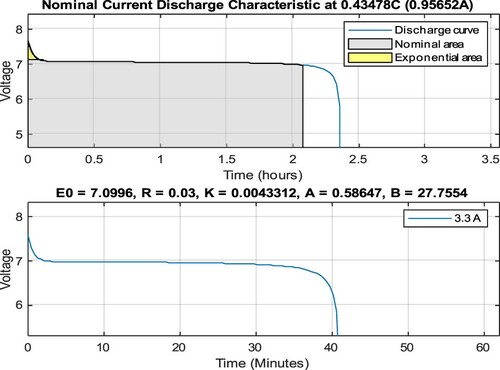
Figure shows the schematic of the PSU.
Figure 13. Electrical schematic of the Power Storage Unit.
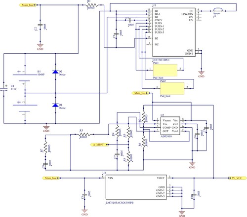
In general, any Power Storage Unit (PSU) design must be following space application standards, such as ECSS-Q-40 [Citation51]. In the proposed electrical schematic shown in Figure , an ADP3310 IC is used as a redundant analogue Battery Charge Regulator (BCR) and analogue MPPT controller. In addition, a UCC3911 IC protection circuit is used against overcharge for the two strings battery. While to meet ECSS standard requirements [Citation52], protection circuit must be taken into account, which is ensured by bypass diode (D1, D2) (MBR1635 Schottky-diodes from ON Semiconductor) against any possible cell damage and electrical insulation between cells to ensure a supply of electrical power to the satellite’s subsystems.
The PCB prototype based on COTS components for the designed PSU is shown in Figure .
Figure 14. Power Storage Unit’s PCB.
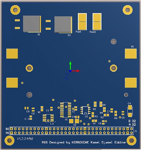
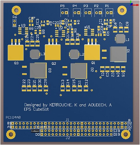
Following the design principles used in CubeSat, the “Plug and Play” method is first applied for PCB electrical connections based on the PC104 standard [Citation23,Citation53]. Then, a set of four holes is also provided for fixing the PSU with the CubeSat structure, and other additional holes are used for fixing the battery (two accumulators) with the PCB of the PSU. The design rules for this PCB comply with ECSS and IEEE standards [Citation54,Citation55].
4.3. Power Regulation Unit
The electrical circuit of the boost converter is shown in Figure .
Figure 15. Electrical circuit of DC-DC boost converter connected with solar panels.
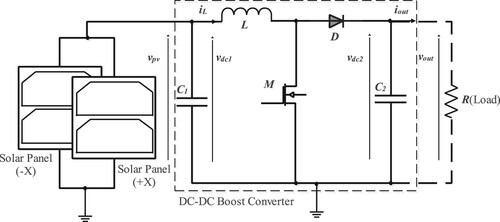
In this electrical circuit of DC-DC boost converter (Figure ), L is the inductance, the power switch M is the MOSFET transistor, and D is the diode. C1 and C2 are the input and the output capacitors.
Based on the electrical circuit shown in Figure , the boost converter can be modelled by a unique system of equations; considering the perfect switches assumption, the instantaneous model is given by [Citation56]:
(4)
(4)
(5)
(5) Where
the switch
is closed and
is open.
The expressions of the inductor current, the resistance, the inductance, and the capacitances of the input and output capacitors are resumed in Table ; all expressions are based on a small ripple approximation calculation during a switching period Ts.
Table 5. Boost converter parameter expressions for high and low duty cycles.
Both input and output voltages ripple ΔV are fixed at 2% according to [Citation52]. During the sunlight period, the PV solar panels supply the main power bus via the boost converter; therefore, two characteristics can be distinguished:
Input characteristics: from the connection of the PV panel previously described, considering the voltage drop in the diode, which can reach the maximum voltages included in the interval between 3.3–4.3V (with the consideration of the voltage drop over the blocking diode).
Output characteristics: In the main power bus, the voltage level varies slowly between 6.6-7.2V due to the changes in the battery charge condition.
Table 6. Parameters of boost converter obtained from the high and low duty cycle.
When calculating the boost converter parameters, the larger value is chosen as design philosophy, to tolerate the components to withstand the span of the whole Duty cycle (D) values. This condition must be fulfilled to avoid Discontinuous Conduction Mode (DCM). Therefore, in this design procedure, the DCM is verified for the chosen D as shown in Table .
Table 7. DMC verification of boost converter obtained for high and low duty cycle.
The simulation results of the boost converter with high and low duty cycles are shown in Figure .
Figure 16. Simulation of the boost converter with high duty cycle and low duty cycle: (Dashed line) Output currents; (Solid line with dots) Output voltages.
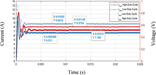
From the results obtained by simulation with a high duty cycle, it is observed that during the steady-state, the current value is approximately 0.57A and the voltage value is approximately 7.2V. Moreover, for the simulation results obtained with a low duty cycle, it is noticed that the current is 0.62A and the voltage is 6.5V. It can also be seen that the converter never goes in DCM even in the startup with the high over-shoot for both low and high duty cycles.
Based on the proposed EPS architecture shown in Figure , the electrical circuit design schematic corresponding to the Power Regulation Unit, boost converter based, is shown in Figure , which is then used to work out the PCB design with appropriate component footprints in Figure .
Figure 17. Electrical schematic of the Power Regulator Unit-based boost converters.
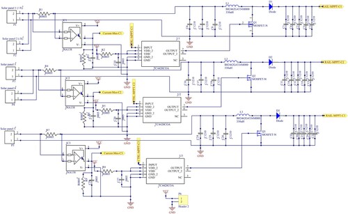
Figure 18. Power Regulation Unit’s PCB.
The electrical schematic shown in Figure is built by the COTS components [Citation57], established on results reported in Table . The MOSFET IRFZ24NS/L from “International Rectifier” is selected, which is driven by TC4420 power driver from “Microchip”. The input and output voltages measurements are ensured by the voltage divider. While the input currents are measured by the high-side shunt monitor INA138 from “Texas Instrument”. To reduce the effect of the voltage drop, Schottky diodes (MBR1635 from “On Semiconductor”) are used. The solar panels are connected using 2 pins connectors. The header PC104 ensures the power, measurements, and control lines [Citation58].
4.4. MicroController Unit
First, the software design to be implemented in the MicroController Unit (MCU) is quite critical and must be carefully defined. In this application, the coded algorithm is based on the Maximum Power Point Tracking (MPPT) and Battery Charge Regulation (BCR) technique. The flowchart of this algorithm is shown in Figure .
Figure 19. Flowchart of power regulation algorithm based on MPPT and BCR implemented in MCU.
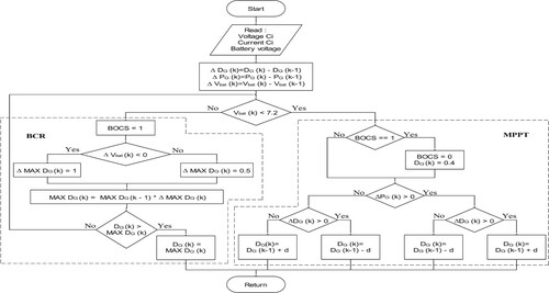
The proposed MPPT is based on Perturb and Observe (P&O) method, where it disturbs the duty cycle by slight increments of operating voltage and observes the variation of power. Then, when the variation of power is positive, it means that the operating voltage is moving to the MPP. At that time, in the same direction as the observed power, a new voltage perturbation will be created. When the algorithm observes a negative power change, the perturbation will move back to the previous operating voltage to retain it at the MPP. On the other hand, due to the resistance instability of the PV panel, the MPP can oscillate during the time [Citation59]. The software BCR technique consists to limit the battery voltage at rated value, as hot redundancy, to prevent battery overcharge so that extending its lifetime.
This control strategy requires some input variables (current and voltages), output variables (Duty cycle (D)), and adequate parameters adaptation (D step size). Therefore, for the MPPT algorithm, certain considerations must be taken into account to define the D interval between measurement points and the frequency at which the algorithm should be executed. Since the proposed MPPT algorithm assumes a stable input current, it cannot make a new measurement, until the converter is stabilized. So that, a minimum step size (d) has to be calculated following MPP variation as given below:
(6)
(6) Where
is related to the boost converter switching speed which depends on the transient response and its settling time responding to a step input. The boost converter switching speed is about 200Hz deduced from Figure . The MPP voltage is likely to vary from 3.6–4.6V during one minimum/maximum cycle; thus, two changes are found for each 360° turn cycle (one for each solar panel). The maximum and minimum duty cycle is likely to be 0.34 and 0.54, respectively, (see section boost sizing and design). According to [Citation60], the nanosatellite maximum speed (
) will be about 3 rounds per minute.
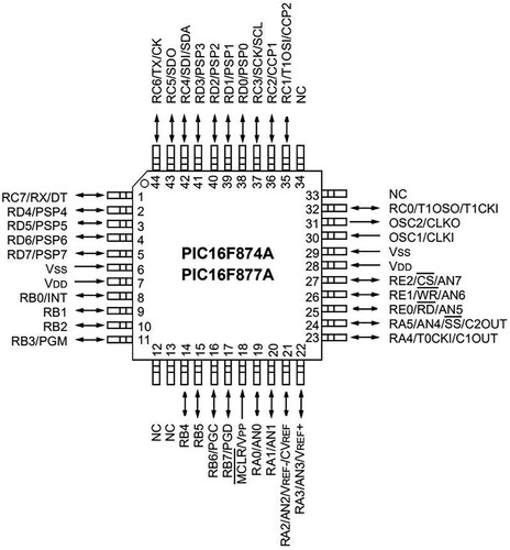
The MCU PIC16F877A hardware is chosen for the software implementation of the power regulation algorithm presented in Figure . In addition to the space heritage and low cost [Citation61–63], this MCU comes with many technical features that make it a good design trade-off, such as:
A built-in Analogue to Digital Converter (ADC) also satisfy the current and voltage sensors number, so no need to add multiplexers or external ADC [Citation61,Citation62].
An appropriate built-in module for Pulse Width Modulation (PWM) to control the boost converters,
The third feature is the existence of the I2C communication protocol, which is the reason behind choosing the PIC16F877A for the communication interface with OBDH,
It also contains a full-speed and low-speed compatible RS-232 Serial Interface Engine (SIE) that allows fast communication between an external host device and the PIC MCU [Citation64].
Figure 20. Simulation of MCU circuit programmed with MPPT and BCR functions.
Two types of control signals (PWM) will be used for the boost converters; one from the MCU and another generated by the IC DP3810 (see Figure ). A sort of selection/arbitration system is needed to decide which MPPT signal will drive the converter. In case of MCU failure, cold redundancy is used for the MPPT technique. As shown in Figure , the decision was made to use the 6->3 multiplexer as an arbitrating system based on the IC 74HCT4052, controlled by the MCU. When the MCU hangs or crashes and will be unable to control the multiplexer, the address to the multiplexer is changed and the analogue MPPT (ADP3810) signal is switched (see the truth table on Table ) to control the boost converter.
Figure 21. Simulation of MCU failure case: Boost converter driven by PWM signal from analogue MPPT selected by the arbitrating system.
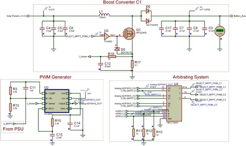
Table 8. Truth table of arbitrating system for cold redundancy.
5. EPS experimental verification
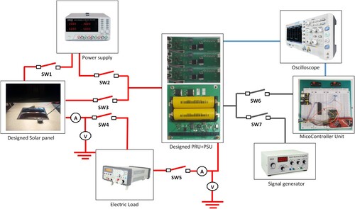
This section describes the experimental testing flow conducted on each part of the designed EPS (namely: Solar panel, PSU, PRU, and MCU) to verify the effectiveness of the proposed design procedures using the Electrical Test Bed (ETB) as shown in ON/OFF devices/switches (SW1 to SW7), which are used to permit testing each EPS part separately (Figure ).
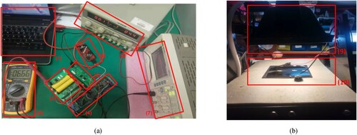
Figure 22. EPS design ETB: (a): (1): Computer; (2): Voltmeter; (3): Battery and Power Storage Unit; (4): MCU; (5): Power Regulation Unit; (6): Programmer and Debugging system; (7): Oscilloscope; (8) Power supply; (b): (9) Lighting system; (10): Assembled solar panel.
5.1. Solar panels test
Solar panels testing is a process aimed to determine any mechanical damage or electrical degradation that may avoid the use of the item as a flight module following ECSS requirements [Citation67]. The process is conducted at cell level as well as panel level depending on the manufacturing phase.
A visual inspection is firstly done on each solar cell to spot out any damages, such as cracks or portion defects. The solar cells that pass the test are then selected for additional testing discussed below.
5.1.1. Electroluminescence Test
To perform the Electroluminescence (EL) test on the solar panel, the switch SW1 is turned ON to connect the regulated power supply to the solar panel (see Figure ). For this purpose, each cell was exposed to the EL testing throughout the integration process. The EL test is a qualitative inspection conducted on large photovoltaic cells [Citation68]. The experiment is based on the same principle as a Light Emitting Diode (LED); it is a practical and non-destructive method of solar cell's visual assessment for the effects of the damage. This test provides a wealth of data about any manufacturing defects or handling damages spotted out via the area uniformity of solar cells. EL test is very effective in identifying each cell mismatch in PV solar panels as cracks, portion defects, and material variations are quickly and non-destructively identified. This type of crack most likely occurred during the manufacturing process and would not be detected in the I-V curves obtained by illumination tests (Section V. A.2) as they do not result in a significant drop in cell performance. With time mission and temperature variations, these cracks are likely to spread and cause degradation in performance.
Figure 23. Line-up test block diagram of all EPS parts.
In this experimentation, a voltage is supplied to a solar cell gradually increased in a forward bias configuration until the cell lights up. Figure shows the results of the EL testing for solar cells and solar panel.
Figure 24. EL testing: (a) one solar cell, (b) one solar panel.
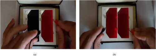
As shown in Figure (a), electroluminescence is caused on the solar cell when the supplied voltage has reached 2.3V and the current has been set to 100mA. Then, the same test was performed on a solar panel composed of two cells, as shown in Figure (b), where this time the solar panel starts to light up when the supplied voltage reaches 4.6V and the current has been set to 100mA. Usually, the dark spots reveal damage to the solar cells while the low light alerts on the degradation of the solar cells before the integration process. Degraded solar cells have a lower intensity EL signal confirming partial cell shading. The EL test can also reveal microcracks that do not significantly affect the output power of the solar panel (obtained by an illumination test) but could over time cause serious damage. Following the visual inspections of Figure (a,b) obtained by the EL tests, the solar cells are very well lighting, which means they are in good working condition and can also be used for the CubeSat flight model. In addition, according to Figure (a,b), by visual checks, there is no presence of microcracks, which confirms that the solar cells used have excellent performance without degradation.
5.1.2. Illumination test
The test aims to analyze the electrical performances and to generate the characteristic curves (I(V) and P(V)) of the solar panel. The proposed illumination test of the solar panel is shown in Figure . According to the schematic diagram test, only the switch SW4 must be set ON to connect the solar panel to the variable electrical load.
The I(V) curves are the most helpful tool used to identify the cell and panel characteristics. These include, in particular, but are not limited to, short circuit current, open-circuit voltage, maximum power output, spectral response, fill factor, series resistance, and temperature coefficients. Measuring solar panels requires a stable light source that closely matches the sunlight’s conditions. The test bench used to carry out the initial measurements, (Figure (b)) is built with an available low-cost Tungsten-Halogen lamp [Citation69], as a source of light of 500W, placed just 25cm over the PV solar panel. This short distance is well defined, to improve the illumination non-uniformity and to leave a distance to avoid the heating of solar cells because at the same time the PV panel is exposed to light and heat; the absorptivity of the PV panel is very high (≤ 0.91). Therefore, the PV cells’ temperature rises to achieve 60°C. The I(V) and P(V) characteristics of the assembled solar panel obtained from the illumination test are shown in Figure .
Figure 25. Solar panel characterization obtained from illumination test.
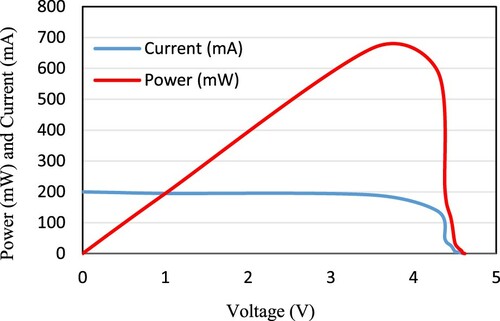
As shown in Figure , the power characteristic of the solar panel reached the maximum of 680mW at the voltage of 3.6V, and the current short circuit reached the value of 200mA under a temperature of about 60°C and the irradiance of 500W. From this experiment, it can be noticed that the designed solar panel can produce enough energy at low irradiance and can also produce more at higher irradiance.
5.2. Power Storage Unit test
The proposed experiment for testing the PSU is presented in Figure . To perform this test, according to the schematic block diagram, only the switches SW2 and SW5 need to be set ON to connect the regulated power supply to the PSU during the charging process, and connect the variable electrical load to the PSU during the discharging process.
The PSU and the included battery have been verified under the following test conditions:
Ambient temperature of 28C°,
Charging/Discharging current: 3300mA (one and half of capacity),
Constant Charging voltage: 7.2V,
Charging/Discharging time: around 40min.
Figure 26. Experimental tests of the batteries: (a) charging characteristic; (b) discharging characteristic.
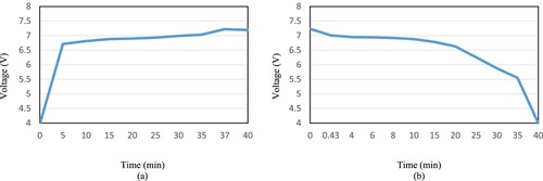
It should be noted that during the charging, the battery voltage is accurately controlled to not exceed the voltage nominal value. So that, a protection circuit incorporated in the PSU is used for this purpose. When discharging the battery, the result obtained from this test is similar to that obtained by simulation (see Figure ). However, the protection circuit disconnects the batteries at Vbat = 6.1V, then the batteries were forced to discharge below this value to stop the test at 4.0V (cut-off voltage).
The battery voltage level and the voltage of the electrical circuits are presented in Figure .
Figure 27. Charged battery level: (a) Battery voltage, (b) Voltage of electrical circuits.
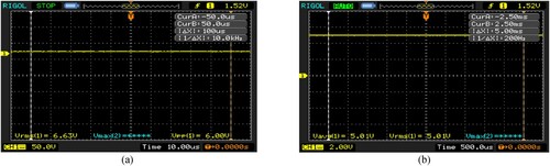
From Figure , when the battery voltage level is at 6.63V, it is shown that the regulator used in the PSU ensures that the voltage of the electric circuit is working well, which gives the accepted voltage level, which is 5V to power the MCU and other circuits.
5.3. Power Regulator Unit test
The proposed experiment for testing the PRU is shown in Figure . To perform this test, according to the test in the schematic diagram, the switches only SW2 and SW6 or SW2 and SW7 need to be set ON to connect the regulated power supply to the PRU and for the connection of the MCU used to generate the PWM signal. The switches SW6 and SW7 have similar signal generation functions and are used for connection with PRU to ensure PWM signal generation.
Based on the simulation of the boost converter (see Figure ) with the available values of the real electronic components, in this experimentation section the input voltages (see Figure ) are updated slightly to be 3.6V and 4.35V, respectively for high and low duty cycles (see Figure ). The high and low duty cycle output voltages are shown in Figure .
Figure 28. (a) Input voltage 3.6V, (b) Input voltage 4.35V.
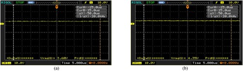
Figure 29. (a) High duty cycle PWM signal, (b) Low duty cycle PWM signal.
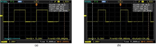
Figure 30. (a) Output voltage obtained by low duty cycle PWM signal, (b) Output voltage obtained by high duty cycle PWM signal.
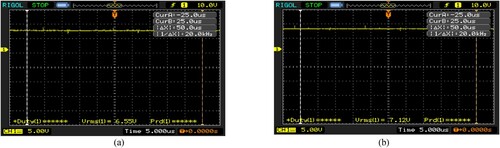
According to the experimental results obtained in Figure and Figure , the values of the output voltages for the low and high duty cycles are 6.55V and 7.12V, respectively. Also note that the voltage signal ripples, for the low and high duty cycles, are very weak. In addition, it can be seen that the boost converter designed with dimensioned parameters avoids DCM and even at start-up there is no overshoot, for both low and high duty cycles. As a result, these output voltages are almost similar to those obtained by simulation (Figure ), confirming that the sizing parameters used in the design meet the EPS requirements in terms of voltage level and low voltage ripples.
5.4. MCU test
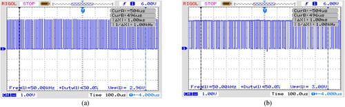
The proposed experiment for testing the MCU is shown in Figure . To perform this experiment, according to the test in the schematic diagram, only the switch SW6 needs to be set ON to connect the MCU for PWM signal generation to the PRU. The oscilloscope is always connected to display and measure the generated PWM signals from the MCU.
The code of the proposed control strategy (MPPT and BCR) was first compiled by MPLAB-X-IDE software and then uploaded to the MCU using Pikit3 hardware. The PWM output signals obtained by the MCU are shown in Figure . The oscilloscope plots (Figure ) confirm that the MCU executed the task without difficulties (low and high PWM signals) and this revealed that the MCU, as well as the development tool and the code downloader, did perform their tasks very well. The PWM signal generated by the MCU is similar to that obtained by simulation and to that generated by the signal generator equipment; therefore, the software implemented in the MCU meets the design requirements.
Figure 31. Output PWM obtained by MCU: (a) Low duty cycle PWM signal, (b) High duty cycle PWM signal.
6. EPS cost evaluation
Cost is always the main critical factor in any design process, as it applies to a CubeSat project. The cost analysis determines a critical gap in the estimation of the costs of nanosatellites, from the literature [Citation70,Citation71], which was observed by comparison between two cost models, the Small Satellite Cost Model (SSCM <50kg) and the NASA/Air Force Cost Model (NAFCOM). Each of these models provides a basic understanding of the elements that go into cost estimation. While to accurately reflect mission costs, Cost Estimating Relationships (CERs) lack sufficient historical data on picosatellites and nanosatellites (50 kg). Because precise cost models require taking into account complex parameters and integrating different aspects (Student, faculty, travel, and facilities costs) to build a database. Estimating the cost of each system by an approximative and reusable cost analysis is beneficial to future system design teams who can use the reusable design without wasting time, money, and energy determining the costs involved. In this paper, an assessment of the total cost of the EPS is required at the early stages of design because managing the cost reduction of this system at the design stage is more effective than at the manufacturing and development stage. 70–80% of the cost of the product is determined during the design phase according to several authors [Citation72,Citation73]. In this project, the CT factor is calculated simply by:
(7)
(7) Where CTi representing the cost of each component and therefore CT representing the total cost of the concept. Based on the available online markets [Citation74–78], the total cost of each EPS unit is presented in Table .
Table 9. Costs of EPS units.
Nowadays, it is possible to find good commercial EPS products provided by space companies. However, designing one is an interesting cost-effective trade-off and a good teaching process for CubeSat engineers at the same time. In this study, the second option is preferred; the following charts (Figure ) are for the distribution cost of solar panel, PSU including the batteries, PRU, and MCU respectively.
Figure 32. Distribution cost: (a) Solar panel, (b) PSU, (c) PRU and (d) MCU.
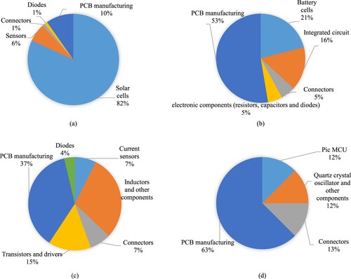
From the distribution cost of the EPS presented in Figure , it is noticed that solar cells are the most expensive component [Citation25]. These prices have been evaluated to the available markets, which depend on many factors such as the quantities purchased and their availability. In this paper, EPS costs related to assembly, integration, testing, and verification are not taken into account.
7. Conclusion
The main objective of this paper is to provide sufficient basic knowledge about certain methods and techniques to enable students and new space engineers to design EPS for nanosatellites on their own without the extra costs related to the standard commercial purchase. Firstly, this paper defined the objectives, the mission requirements, and how to derive them into power system specifications to propose the most suitable and reliable electrical architecture to achieve the successful mission of the CubeSat. The proposed design method will facilitate moving from preliminary to detailed design and will allow flexible iterative experimental validation to have the appropriate EPS design, for the engineering model and the space-qualified model as well.
The dedicated space-grade components are expensive and not easily available. Consequently, all the electronic components used in this project should be low-cost Commercial-Off-The-Shelf (COTS). However, the components based on a semiconductor must have space qualifications or be shielded from the radiation and be robust during the whole mission. In this design approach of the proposed EPS, the selection of components was based on COTS experienced and used in successfully launched nanosatellites, especially during maximum solar activity periods which produce high radiation [Citation79,Citation80]. The typical Total Ionization Dose (TID) for nanosatellites, in LEO missions below the internal radiation belt, is only around 5-10krad, which most newer COTS parts can inherently tolerate. Therefore, the tolerated value of a TID over a specific duration (one year) will be significantly lower than 5krad, which is considered safe for COTS components [Citation81,Citation82]. Moreover, upon choosing the required design elements, an efficiency assessment based on simulations and experimentation is mandatory established to guarantee their suitability for the initial assumption. In this design, both analog Integrated Circuit (IC) and digital MicroController Unit (MCU) are considered as cold/hot redundancy approaches to improve the design reliability. As a hot redundancy strategy, battery charge regulation is implemented in an MCU and operated by an analog IC; the same IC is used for the maximum power point tracking which is also combined in the same algorithm implemented in the MCU as cold redundancy.
According to the experimental verification, the tested solar cells are in good health and can produce the required energy. Thus, in terms of energy produced, the designed solar panel can accomplish the CubeSat mission. Likewise, the power storage unit performed very well, as evidenced by the battery charge and discharge characteristics achieved. The power converters used in the power regulation unit with the proposed control algorithm are also functioning very well and matching the simulation results. Therefore, the effectiveness of the proposed EPS design was proven to be capable of supplying the CubeSat subsystems.
The designed EPS prototype proposed in this work is used as an engineering model; for the space-qualified model, some ideas must be taken into consideration in the upcoming work of this designed EPS as follows:
Make sure to fulfil the recommended environmental qualification (using an ElectroMagnetic Compatibility (EMC) chamber, mechanical vibration, and a thermal vacuum chamber) to decide whether the designed EPS modules are qualified for space or not, so, more luck in the launch opportunity [Citation83],
Come up with more hardware solutions and testing to improve protection against space radiations that are very harmful to the electrical circuits and components on the CubeSat, such as “single event latch-up and total ionization dose” in the semiconductor devices [Citation84] that can burn the component if the power is not turned off quickly enough [Citation85,Citation86],
Consider conducting real-time simulations/measurements of subsystems using Hardware In Loop (HIL) for different scenarios when the CubeSat is simulated in its orbit [Citation87],
Conduct comparative analysis between analogue and digital MPPT by using different microcontroller technologies in terms of the overall efficiency and reliability of the EPS.
Disclosure statement
No potential conflict of interest was reported by the author(s).
Additional information
Funding
References
- R. A. Joost Elstak, Robert Hamann. A comparative analysis of project management and systems engineering techniques in CubeSat projects; 2009.
- Elsaesser A, Merenda F, Lindner R, et al. Spectrocube: a European 6U nanosatellite spectroscopy platform for astrobiology and astrochemistry. Acta Astronaut. 2020;170:275–288.
- Sanchez H, McIntosh D, Cannon H, et al. Starling1: Swarm technology demonstration; 2018.
- Hand E. “Interplanetary small satellites come of age,” ed: American Association for the Advancement of Science; 2018
- Rutter L, Barker R, Bezdan D, et al. A new era for space life science: International standards for space omics processing. Patterns. 2020: 100148.
- Millan RM, Von Steiger R, Ariel M, et al. Small satellites for space science: A COSPAR scientific roadmap. Adv Space Res. 2019;64(8):1466–1517.
- Garcia-Cuadrado G. Nanosatellites-the tool for a new economy of space: opening space Frontiers to a wider audience. J Aeronautics Aerospace Eng. 2017;6(2):1–11.
- Selva D, Golkar A, Korobova O, et al. Distributed earth satellite systems: what is needed to move forward? J Aerospace Inform Syst. 2017;14(8):412–438.
- Oberholzer JF, Uheida E, Oosthuizen G. Resource efficient process chain development of a modular CubeSat spaceframe. Proc Manufact. 2019;35:917–928.
- Wachowicz ME, Bury M. Space technology transfer problems in the context of protecting the space heritage. Space Policy. 2017;42:66–69.
- Denis G, Alary D, Pasco X, et al. From new space to big space: How commercial space dream is becoming a reality. Acta Astronaut. 2020;166:431–443.
- Bôas DJFV, Souza CHM, da Motta Silva F, et al. Proposal of low cost launchers for scientific missions using cubesats. Adv Space Res. 2020;66(1):162–175.
- Woellert K, Ehrenfreund P, Ricco AJ, et al. Cubesats: cost-effective science and technology platforms for emerging and developing nations. Adv Space Res. 2011;47(4):663–684.
- Del Corso D, Passerone C, Reyneri L, et al. Design of a university nano-satellite: The PiCPoT case. IEEE Trans Aerospace Electron Syst. 2011;47(3):1985–2007.
- Cho M, Masui H, Satellite K. Nano-satellite development project and space engineering education at Kyushu Institute of Technology. In: 2013 6th International Conference on Recent Advances in Space Technologies (RAST): IEEE; 2013. p 1059–1063.
- Roman-Gonzalez A, Quiroz-Olivares AE, Vargas-Cuentas NI. Advances in the UCHSat-1 nanosatellite: design and simulation. Adv Astronautics Sci Technol. 2020;3(1):65–74.
- Rodríguez J, Laverón-Simavilla A, del Cura JM, et al. Project based learning experiences in the space engineering education at technical University of Madrid. Adv Space Res. 2015;56(7):1319–1330.
- Walker R, Galeone P, Pageet H, al. “ESA hands-on space education project activities for university students: Attracting and training the next generation of space engineers,” In IEEE EDUCON 2010 Conference: IEEE. p. 1699–1708; 2010.
- Nieto-Peroy C, Emami MR. Cubesat mission: from design to operation. Appl Sci. 2019;9(15):3110.
- Kulu E. Nanosatellite Database. http://www.nanosats.eu/index.html#database; 2019.
- Noca GRM, Jordan F, Scheidegger N, et al. Mission, Space and Ground System Overview. In: Phase B/C Delta-PDR Project, UNINE / HES-SO/EPFL Lausanne Switzerland, 24/08/2007.
- Ali A, Mughal MR, Ali H, et al. Innovative power management, attitude determination and control tile for CubeSat standard nanosatellites. Acta Astronaut. 2014;96:116–127.
- Bouwmeester J, Langer M, Gill E. Survey on the implementation and reliability of CubeSat electrical bus interfaces. CEAS Space J. 2017;9(2):163–173.
- Alanazi A, Straub J. Engineering Methodology for student-driven CubeSats. Aerospace. 2019;6(5):54.
- M. R. Patel, Spacecraft power systems. CRC Press, 2004.
- Seddjar A, Kerrouche KDE, Wang L. Simulation of the proposed combined Fuzzy Logic Control for maximum power point tracking and battery charge regulation used in CubeSat. Arch Electr Eng. 2020;69(3).
- Gonzalez-Llorente J, Rodriguez-Duarte D, Sanchez-Sanjuan S, et al. Improving the efficiency of 3U CubeSat EPS by selecting operating conditions for power converters. In: 2015 IEEE Aerospace Conference: IEEE; 2015. p. 1–7.
- Wertz WJLAJR. Space Mission Analysis and Design; 1999. p 412–415.
- ECSS-E-TM-E-10-25A E. S. E.-E. R. S. Division. Noordwijk, The Netherlands, 20 October 2010.
- Larson WJ, Wertz JR. Space mission analysis and design. Torrance (CA): Microcosm; 1992.
- e. Clyde Space Ltd. User manual: CubeSat 3U Electronic Power System CS-3UEPS2-NB. 22 Oct. 2014.
- Schirone L, Macellari M, Schiaratura A. Modular power conversion systems for body-mounted solar panels. In: Proc. 8th European Space Power Conference; 2008.
- Oredsson M. Electrical power system for the CubeSTAR nanosatellite; 2010.
- Kerrouche KDE, Wang L, Bendoukhad SA, et al. Reliable protection strategy of power distribution module for university CubeSat. In: Fifth IAA Conference on University Satellite Missions and CubeSat Workshop Rome, Italy 2020, vol. 173, Advances in the Astronautical Sciences ed. [Online]. Available: http://www.univelt.com/book=8071.
- Sera D, Mathe L, Kerekes T, et al. On the perturb-and-observe and incremental conductance MPPT methods for PV systems. IEEE J Photovolt. 2013;3(3):1070–1078.
- Lyden S, Galligan H, Haque ME. A hybrid simulated annealing and Perturb and observe maximum power point tracking method. IEEE Syst J. 2020.
- 30% Triple Junction GaAs Solar Cell Assembly. Type: TJ solar cell assembly 3G30A, improved voltage at maximum power point. [Online]. Available: www.azurspace.de.
- Aoudeche A, Zhao X, Kerrouche KD. Design of a high performance electrical power system for an earth observation nano-satellite. In: Proceedings of the 2018 international conference on electronics and electrical engineering technology: ACM, p. 140–146; 2018.
- Faiza A, Eddine Kamel KD. Design of electrical power system for low-cost ecological nanosatellite.
- Veerachary M, Senjyu T, Uezato K. Voltage-based maximum power point tracking control of PV system. IEEE Trans Aerospace Electron Syst. 2002;38(1):262–270.
- Miyatake M, Veerachary M, Toriumi F, et al. Maximum power point tracking of multiple photovoltaic arrays: A PSO approach. IEEE Trans Aerospace Electron Syst. 2011;47(1):367–380.
- Balato M, Costanzo L, Marino P, et al. Modified TEODI MPPT technique: theoretical analysis and experimental validation in uniform and mismatching conditions. IEEE J Photovolt. 2016;7(2):604–613.
- Asundi S, Mahin M, Nagabhushan V, et al. Composite and PCB based implementations of a solar panel design for SwampSat. In: 24th Annual AIAA/USU Conference on Small Satellites, Logan, Utah, United States; 2010.
- Chin KB, Brandon EJ, Bugga RV, et al. Energy storage technologies for small satellite applications. Proc IEEE. 2018;106(3):419–428.
- Cook R, Swan L, Plucknett K. Failure mode analysis of lithium ion batteries operated for low Earth orbit CubeSat applications. J Energy Storage. 2020;31:101561.
- High Power Lithium Ion APR18650M1A. [Online]. Available: www.a123systems.com.
- Hu X, Li S, Peng H, et al. Robustness analysis of state-of-charge estimation methods for two types of Li-ion batteries. J Power Sourc. 2012;217:209–219.
- Reddy TB. Linden's handbook of batteries. New York: Mcgraw-hill; 2011.
- Knap V, Vestergaard LK, Stroe D-I. A Review of battery technology in CubeSats and small satellite solutions. Energies. 2020;13(16):4097.
- Clark C, Simon E. Evaluation of lithium polymer technology for small satellite applications; 2007.
- ECSS-Q-40B, SPACE PRODUCT ASSURANCE, SAFETY (17-AY-2002). ESA. [Online]. Available: http://everyspec.com/ESA/ECSS-Q-40B_9522/; 2018.
- ECSS-E-ST-20C. Space engineering electrical and electronic, E. S. E.-E. R. S. D. Noordwijk, The Netherlands 31 July 2008.
- Voss D, Coombs J, Fritz T, et al. A novel spacecraft standard for a modular nanosatellite bus in an operationally responsive space environment. In: 7th Responsive Space Conference. p. 1–11; 2009.
- Novak F, Biasizzo A. Security extension for IEEE Std 1149.1. J Electron Test. 2006;22(3):301–303.
- ECSS-Q-ST-70-12C – Design rules for printed circuit boards, 14 July 2014.
- Rekioua D, Matagne E. Optimization of photovoltaic power systems: modelization, simulation and control. Cham: Springer Science & Business Media; 2012.
- Hunyadi G, Klumpar DM, Jepsen S, et al. A commercial off the shelf (COTS) packet communications subsystem for the Montana EaRth-Orbiting Pico-Explorer (MEROPE) CubeSat. In: Aerospace Conference Proceedings, 2002. IEEE, vol. 1: IEEE. p. 1; 2002.
- Go S, Bouwmeester J, Brouwer G. Optimized three-unit cubesat structure for Delfi-n3Xt. In: Proceedings of the 59th International Astronautical Congress, Glasgow, Scotland; 2008.
- Durgadevi SAA, Natarajan SP. Study and implementation of maximum power point tracking (MPPT) algorithm for photovoltaic systems. In: Presented at the in 1st International Conference on Electrical Energy Systems; 2011.
- Vinther K, Jensen KF, Larsen JA, et al. Inexpensive cubesat attitude estimation using quaternions and unscented Kalman filtering. Autom Contr Aerospace. 2011;4(1):1–12.
- Ahmed BS, Szasz B, Masanori N. Control system design of an ultra-small deep space probe. Energy Proc. 2016;100:537–550.
- Kuroiwa F, Bendoukha SA, Okuyama K-I, et al. A redundancy and operation of power control system for a deep-space small probe. J Autom Contr Eng. 2016;4(5):353–359.
- Kuroiwa F, Okuyama Ki, Nishio M, et al. A design method of an autonomous control system for a deep-space probe. Trans Jpn Soc Aeronautical Space Sci. 2016;14(30):105–112.
- PIC16F87XA. 28/40/44-Pin Enhanced Flash Microcontrollers.
- Smith DW. PIC in Practice: A project-based approach. Newnes; 2006.
- T. Instrument. INA1(8 high-side measurement current shunt monitor). [Online]. Available: www.ti.com/legal/termsofsale.html.
- ECSS-E-ST-20-08C Rev.1 Space engineering, E. S. E.-E. R. S. Division. Noordwijk, The Netherlands, 18 July 2012. [Online]. Available at http://everyspec.com/ESA/download.php?spec=ECSS-E-ST-20-08C_REV-1.047905.pdf.
- Fontani D, Sansoni P, Francini F, et al. Electroluminescence Test to investigate the humidity effect on solar cells operation. Energies. 2018;11(10):2659.
- Namin A, Jivacate C, Chenvidhya D, et al. Construction of tungsten halogen, pulsed LED, and combined tungsten halogen-LED solar simulators for solar cell-characterization and electrical parameters determination. Int J Photoenergy. 2012;2012:1–9.
- Broder M, Mahr E, Barkmeyeret D, al. Review of three small-satellite cost models. In: AIAA SPACE 2009 conference & exposition. p. 6689; 2009.
- Stahl HP. Survey of cost models for space telescopes. Opt Eng. 2010;49(5):053005.
- Corbett J, Crookall J. Design for economic manufacture. CIRP Ann. 1986;35(1):93–97.
- Mileham A, Currie G, Miles A, et al. A parametric approach to cost estimating at the conceptual stage of design. J Eng Design. 1993;4(2):117–125.
- Worldway Electronics Limited. https://fr.bomeasy.com/pro/microchip-technology/16f877a-ip/2811281 (accessed 2/8/2021).
- Mouser Electronics, Inc. https://www.mouser.fr/new/3m/3mpc104/ (accessed 02/08/2021).
- batt-energy-shop. https://www.batt-energy-shop.de/Akkus/Lithium-Akkus/A123-Systems-APR18650M1–LiFePO4-3-3V-1100mAh.html?language = en (accessed 02/08/2021).
- high quality pcb. https://www.hqpcb.com/ (accessed 02/08/2021).
- AZUR SPACE Solar Power GmbH. http://www.azurspace.com/index.php/en/products/products-space/space-solar-cells (accessed 02/08/2021).
- Suparta W, Zulkeple SK. Investigating space radiation environment effects on communication of Razaksat-1. J Aerospace Technol Manag. 2018;10:1–12.
- Aguilar AC. Characterization of commercial step-down converter performance in the low Earth orbit radiation environment. Massachusetts Institute of Technology; 2019.
- Budroweit J, Patscheider H. Risk assessment for the use of COTS devices in space systems under consideration of radiation effects. Electronics (Basel). 2021;10(9):1008.
- Hodson RF, NESC YC, Pandolf JE, et al. Recommendations on use of commercial-off-the-shelf (COTS) electrical, electronic, and electromechanical (EEE) parts for NASA missions. National Aeronautics and Space Administration, Langley Research Center; 2020.
- Monteiro JP, Rocha RM, Silva A, et al. Integration and verification approach of ISTSat-1 CubeSat. Aerospace. 2019;6(12):131.
- Baumann RC. Radiation-induced soft errors in advanced semiconductor technologies. IEEE Trans Device Mater Reliab. 2005;5(3):305–316.
- Boscherini M, et al. Radiation damage of electronic components in space environment. Nucl Instr Methods Phys Res Sect A Acceler Spectrom Detect Assoc Equip. 2003;514(1-3):112–116.
- Maurer RH, Fraeman ME, Martin MN, et al. RHarsh environments: space radiation. Johns Hopkins APL Techn Dig. 2008;28(1):17.
- Kiesbye J, Messmann D, Preisinger M, et al. Hardware-in-the-loop and software-in-the-loop testing of the move-ii cubesat. Aerospace. 2019;6(12):130.
Appendix
shows the electrical characteristics of solar cells:
Table A1. Electrical characteristics of solar cells [Citation37].
Table A2. Electrical characteristics of battery cells [Citation46].
Figure A1. PIC16F877A pin connections.
shows the acronyms list.
Table A3. Acronyms list.