
 ?Mathematical formulae have been encoded as MathML and are displayed in this HTML version using MathJax in order to improve their display. Uncheck the box to turn MathJax off. This feature requires Javascript. Click on a formula to zoom.
ABSTRACT
This article proposes a dual space vector PWM control technique for a three-phase to five-phase quasi Z-source direct matrix converter (QZSDMC). The proposed circuit consists of a quasi-impedance source network along with a five-phase traditional matrix converter. With the observation of bidirectional operating capability and the utilization of shoot-through duty ratio, the proposed converter can ensure both buck and boost operations. This converter overcomes the voltage transfer ratio restriction and poor voltage regulation of the traditional matrix converter. Also, this converter ensures continuous input current with an absence of input LC filter components. The proposed direct AC to AC power converter gives an alternate solution to the multiphase drive system instead of the traditional voltage source inverter. The developed dual space vector PWM control technique for three-phase to five-phase voltage conversion is derived from the basic space vector PWM approach. The proposed dual space vector PWM technique utilizes 90 active states and 3 zero vector states among 243 switching states. The QZSDMC has been analysed with a dual space vector PWM approach along with the distribution of shoot-through state in the zero vector. The proposed topology along with the control strategy has been simulated using MATLAB/Simulink environment.
1. Introduction
The matrix converter is a bidirectional power flow converter. It’s consisting of semiconductor switches. The switches are arranged like an array or matrix [Citation1]. Recently, the matrix converter attracted more researchers based on its features and advantages such as sinusoidal input and output currents, controlled bidirectional power flow, and operation at unity power factor for all loads [Citation2,Citation3]. The control algorithm plays a major role in the performance of power electronics converters such as AC to AC or AC to DC to AC [Citation4]. There are many modulation schemes are developed for three-phase or more output-based voltage source inverters. In general modulation schemes for matrix, converters are more complex and it's classified based on the circuit configuration like direct and indirect matrix converters [Citation5]. Alesina and Venturini developed a direct PWM control technique for a direct matrix converter (DMC). Initially, this modulation scheme limits the output as half of its inputs [Citation6]. Using the third harmonics injection PWM scheme, this limit is further extended to 0.866. In the linear modulation region, this limit is realized as maximum for a three-phase to three-phase matrix converter [Citation7].
On the other hand, virtual cascaded connections of the three-phase rectifier, imaginary dc-link capacitor and voltage source inverter act as indirect matrix converters [Citation8]. The presence of bulk intermediate capacitor and inductor bank acts as a filtering component will increase the cost, size, weight and switching losses. Also, the reliability of the converter is poor [Citation9]. To overcome these disadvantages, many researchers are choosing the direct matrix converter (DMC). The main advantages of DMC are the absence of an intermediate DC-link capacitor, low switching losses and higher power conversion ratio [Citation10,Citation11]. The limitation of DMC are the voltage transfer ratio of 0.866, the usage of bidirectional switches are more, poor fault ride-through capability, complex power control strategies, increased common-mode voltages and complicated protection circuits [Citation12,Citation13]. Other operation-related limitations are input side is never to be short-circuited and the output side is never to be open-circuited. It has a complex commutation process as a result, the poor quality output waveform will be getting from the set-up [Citation14,Citation15].
The voltage transfer capability can be increased by two methods. The first method is the usage of a transformer. Again the disadvantages are size and cost is increases, efficiency goes to decreases [Citation16]. The second method is the usage of a matrix reactance frequency converter (MRFC). It has two classifications named as integrated matrix reactance frequency converter (IMRFC) and cascaded matrix reactance frequency converter (CMRFC). Both methods of MRFC have their disadvantages such as poor voltage gain, very low input side power factor, complex control algorithm, and distorted input and output current waveforms [Citation17].
All these disadvantages are overcome by introducing an impedance source-based direct matrix converter (ZSDMC) [Citation18]. The major advantages of this converter are minimum-sized LC components, performing both buck and boost operations, better reliability and higher efficiency, as well as being free from the dead zone. The disadvantages of ZSDMC are, the voltage transfer ratio is 1.15, waveform phase shifting, inaccurate control, higher voltage, and current switching stresses, higher system losses, discontinuous input current and higher input current harmonics [Citation19,Citation20].
To overcome these disadvantages, many researchers focused on a quasi Z-source direct matrix converter (QZSDMC). It overcomes voltage gain limitations and offers up to four to five times higher voltage gain. It has low impulse current, no phase shift, low voltage and current switching stress [Citation21,Citation22]. With the addition of a quasi Z-source into a direct matrix converter, the electromagnetic interferences ability will be enhanced. It offers high-quality waveforms, continuous input currents and less capacitor voltage stress [Citation23,Citation24].
The conventional structure for variable speed drive has a three-phase power electronics converter with a three-phase motor. The matrix converter or voltage source inverter is coming under a modular power electronics converter [Citation25,Citation26]. When the motor is connected to any one of the modular power electronics converters and increases legs automatically many phases go to increases. The development of modular power electronics converters makes a degree of freedom in the number of possible phases [Citation27]. The multiphase motor drives have their advantages over traditional three-phase motor drives. The notable advantages are high-frequency torque pulsation with minimum amplitude, minimum rotor harmonic current losses, minimum DC-link current harmonics, improved system reliability and redundant structure [Citation28,Citation29].
The five-phase motor drive system has several salient features. It’s very attractive to industrial applications. The defense, ship propulsion, traction drive, aircraft and hospital applications required high fault-tolerant property [Citation30,Citation31]. If the number of phases increases automatically volume of the motor drive gets reduced. In naval ships and mining applications, space requirements are very stringent. The five-phase system is more suitable for these applications [Citation32,Citation33]. The British naval ship contains a 15-phase induction motor drive built by Alstom. The machine winding has been reconfigured as 5 three phases or 3 five phases by the application of modular power electronics converters [Citation34,Citation35].
In this paper, the dual space vector PWM-based control strategy is proposed based on the space vector model. The proposed dual SVPWM technique applies for a three-phase to five-phase direct matrix converter cascaded with a quasi-impedance source network. This dual SVPWM is more suitable for digital implementation. In this scheme, the output voltage is enhanced up to four to five times the input voltages. Theoretically, the maximum output magnitude was obtained in the linear modulation region using QZSDMC configurations. This paper presents the simulation result using MATLAB/Simulink environment and the same is validated by experimental prototype set-up. The simulation and experimental results are matched with good feasibility by the suggested QZSDMC topology and its control strategy.
2. QZSDMC: Topology, operation and modelling
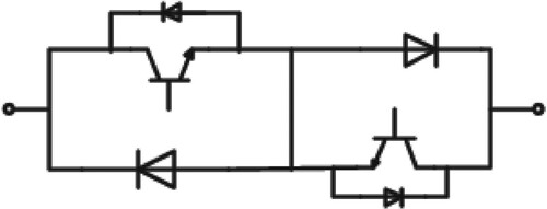
Figure shows the main circuit configuration of QZSDMC. It’s consisting of a three-phase source, input filter, QZS network, direct matrix converter and five-phase RL load. The QZS network consisting of six inductors named Lax, Lbx, Lcx (where x = 1, 2), six capacitors named as Cax, Cbx, Ccx (where x = 1, 2) and three bidirectional switches Sy (where y = a,b,c) with the same switching states, as a result, the switching signal is represented as S0. All inductors having equal values as well as all the capacitors are having equal values [Citation36]. The three-phase to five-phase power circuit topology is connected in series with the Z-source network as presented in Figure . For five-phase, it consists of five legs and each consisting of bidirectional switches. The bidirectional power flow switches consist of two power diodes and two IGBT switches. The power diode and IGBTs are connected in series and the entire switching configuration should be connected in a common-emitter configured bidirectional power flow switch as available in Figure [Citation37]. The output configuration should be odd in phases. The nature of the load connected to the power circuit should be RL load.
Figure 1. Main circuit configuration for three-phase to five-phase QZSDMC.
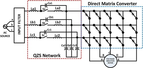
Figure 2. Common-emitter configured bidirectional power flow switch.
The definition for switching function like
Soi = 1 for the switch is in a closed condition
Soi = 0 for the switch is in an open condition
The QZSDMC working principle consists of two states called shoot-through state and non-shoot-through the state. The switch S0 is in an OFF state during shoot through the state as a result the output of QZSDMC is shorted for boost operation. The switch S0 is in an ON state during non-shoot-through the state, and the QZSDMC is working as normal DMC. The equilibrium of the system should be maintained by making all capacitors are equal and all inductors are equal [Citation38,Citation39].
Consider Ts as one switching cycle, consisting of T1 as a shoot-through time interval and T2 as a non-shoot-through time interval. Hence, Ts = T1 + T2 and the shoot-through duty ratio D = T1/Ts. The output voltage equation during shoot through the state can be represented as
(1)
(1)
The output voltage equation during non-shoot-through the state can be represented as
(2)
(2)
During the steady-state condition over one switching cycle in the inductor, the average voltage is zero [Citation40,Citation41]. The symmetrical voltages across three-phase capacitors are
(3)
(3)
The boost factor B for ZSDMC can be expressed as
(4)
(4)
The boost factor B for QZSDMC can be stated as
(5)
(5) where Vo is the amplitude of output voltage and Vi is the amplitude of input voltage.
Thus, the voltage gain “G” for the QZS network using boost factor and modulation index, over one switching cycle is [Citation42]
(6)
(6)
3. SVPMW control algorithm
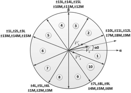
In the space vector plane, the three-phase input current and five-phase output voltages are represented based on the space vector algorithm. In the QZSDMC, there are different switching states are available [Citation43,Citation44]. The switching state represents the connections between the output phases to the input phases. The total numbers of switches including QZS are 18. In that, the main bidirectional switches are 15. The possible combinations of switching states are 215. The following constraints should be followed by QZSDMC for safe switching operations [Citation45,Citation46]. At any switching time do not short circuit at the input side and do not open-circuited at the output side. There are 315 switching combinations are available to satisfy the above-mentioned switching combinations. These 243 possible switching combinations can be categorized into five groups. The combination of switches is represented as [A, B, C], where A, B, C represents the combination of output phases are connected to the input phases a, b, c. The first groups of switching states are zero vectors (i.e. A # B # C [A, B, C € 0, 0, 5]). In this switching state, all the output phases are connected to any one of the same input phases. In the zero vectors, the magnitude and frequency of the output parameters are zero. There are three possible switching combinations are available in this group [Citation47,Citation48].
The second groups of switching states are A # B # C [A, B, C € 0, 1, 4]. In this switching state, any four of the output phases are connected to any one of the same input phases and the remaining one of the output phases is connected to the remaining input phase. One input phase is always not connected to the output phase. There are 30 switching combinations are available in this category. In the space vector, it has a variable amplitude and constant frequency, i.e. amplitude of output voltages depending on the selected input line voltages. In this case, 30 combinations of output voltage and input current space vectors phase angle do not depend on the input voltage and output current phase angle, respectively.
The third groups of switching states are A # B # C [A, B, C € 0, 2, 3]. In this switching state, any three of the output phases are connected to any one of the same input phases and two of the output phases are connected to any one of the remaining input phases. One input phase is always not connected to the output phase. There are 60 switching combinations are available in this category. In the space vector, it has a variable amplitude and constant frequency, i.e. amplitude of output voltages depending on the selected input line voltages. In this case, 30 combinations of output voltage and input current space vectors phase angle do not depend on the input voltage and output current phase angle, respectively [Citation49,Citation50].
The fourth groups of switching states are A # B # C [A, B, C € 0, 2, 3]. In this switching state, any three of the output phases are connected to any one of the same input phases and the remaining two output phases are connected to the remaining two input phases. In this case, all the input phases are engaged with any one of the output phases. There are 60 switching combinations are available in this group. In the space vector, it has a variable amplitude and variable frequency. It says that the amplitude of output voltages depends on the selected input line voltages. In this case, the 60 combinations of output voltage and input current space vectors space angle depend on the input voltage and output current space vector space angles. The output voltage and input current space vectors of these 60 combinations do not have prefixed positions. The locus of the space vector forms ellipses at a different orientation. As a result, the phase angle of input and output vectors cannot be controlled, independently. So the space vector modulation for three-phase to five-phase conversion does not consist of this category of switching states.
The fifth groups of switching states are A # B # C [A, B, C € 1, 2, 2]. In this switching state, any two of the output phases are connected to any one of the same input phases, another two of the output phases are connected to any one of the same input phases and the remaining one output phase is connected to the remaining one input phase. In this case, all the input phases are engaged with any one of the output phases. There are 90 switching combinations are available in this group. In the space vector, it has a variable amplitude and variable frequency. It says that the amplitude of output voltages depends on the selected input line voltages. In this case, the 90 combinations of output voltage and input current space vectors space angle depend on the input voltage and output current space vector space angles. The output voltage and input current space vectors of these 90 combinations do not have prefixed positions. The locus of the space vector forms ellipses at a different orientation. As a result, the phase angle of input and output vectors cannot be controlled, independently. So the space vector modulation for three-phase to five-phase conversion does not consist of this category of switching states. As a result, the effective utilization of the active space vectors for the proposed dual SVPWM for three-phase to five-phase QZSDMC is used in only 93 vector combinations [Citation51,Citation52].
4. Dual space vector PWM control strategy
Figure represents the general topology for three-phase to five-phase QZSDMC. The modulation technique effectively used to control the QZSDMC utilizes only 93 active switching vectors instead of 243. Depending on the output contributions, these active switching states can be grouped into four.
Group 1 [A, B, C € 5, 0, 0]. Three vectors come under this category and it's called zero vectors.
Group 2 [A, B, C € 4, 1, 0]. Thirty vectors come under this category and it's called medium vectors.
Group 3 [A, B, C € 3, 2, 0]. Thirty vectors come under this category and it's called large vectors. In this switching state, any two adjacent output phases are connected to the same input phase.
Group 4 [A, B, C € 3, 2, 0]. The remaining 30 vectors come under this category and it's called large vectors. The major difference in these switching states with the previous case is any two alternate output phases are connected to the same input phase (Figure ).
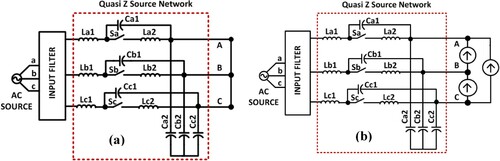
Figure 3. Equivalent circuit of QZSDMC (a) at shoot-through state and (b) at non-shoot-through state.
Figures and represent the input current switching space vectors and output voltage space vectors. Depending on the switching sequences, all the input current space vectors are combined with all the output voltage space vectors. For each combination, the input voltage and current, as well as output voltage and input current space vectors, are defined as
(7)
(7)
(8)
(8)
(9)
(9)
(10)
(10) where Vab, Vbc, Vca are input line voltages; VAB, VBC, VCD, VDE, VEA are output line voltages; Ia, Ib, Ic are input currents; IA, IB, IC, ID, IE are output currents; αi is the input voltage vector space angle; α0 is the output voltage vector space angle; βi is the input current vector phase angle; β0 is the output current vector phase angle.
Figure 4. Group 3: Input current switching space vector.
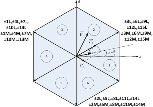
Figure 5. Group 3: Output voltage switching space vector.
Let, M is the medium size space vector; L is the large size space vector; is the desired input line voltage space vector;
is the desired output line voltage space vector;
is the desired input line current space vector;
is the desired output line current space vector and
is the input line to neutral voltage vector, and it’s defined as
(11)
(11)
The proposed space vector control strategy must obey the constraint of unity input power factor for the generation of desired output voltage vectors. So the direction of and
should be the same for obtaining unity input power factor. From Figures and , the identified three-phase input and five-phase output side sectors are 6 and 10, respectively. Consider input and output vectors are in sector-1, the components of
are
(i.e. two adjacent vector directions). Similarly, the components of
. All the output voltage and input current components at sector-1 are given below.
The fundamental SVM algorithm is to select the appropriate switching states and calculate the duty cycle for each switching state during the switching period Ts. To achieve the desired output voltages and input currents, two adjacent switching states should be selected along with zero switching states. This combination will provide maximum output to input voltage transfer ratio. The output voltage and input current vectors can be synthesized by selecting the common switching states. The common switching states are ±10L,±12L,±7M,±9M and ±1L,±3L,±13M,±15M.
The two switching states with the same number with opposite signs, one state should be used based on the duty cycle sign. If the duty cycle is positive, then the positive switching states are used; otherwise, the negative switching states are used if it is negative. From Figures and , the input voltage space vector phase angle is 0 ≤ αi ≤ (π/3) and the output voltage sector phase angle is 0 ≤ α0 ≤ (π/5). In this case, assume line voltage VAB and –VCA are higher values. The large and medium vector configurations are used to obtain the is +10L,−12L,+7M and −9M and for
is +1L,−3L,+13M and −15M. These configurations are associated with the vector directions adjacent to the input current vector positions. Table represents the 60 switching combinations of large and medium vectors for different sectors [Citation53].
Table 1. Space vector choices in SVPWM for various sectors combinations.
Apply the SVM technique and solve the system equation at sector-1, the on-time ratio δ can be calculated for each configuration as
(12)
(12)
(13)
(13)
(14)
(14)
(15)
(15)
(16)
(16)
Consider a balanced three-phase system. The sinusoidal nature supply voltage can be expressed as
(17)
(17)
Now, generate and set the input current vector direction using configurations +10L,−12L and +7M,−9M.
(18)
(18)
Now, generate and set the input current vector direction using configurations +1L,−3L and +13M,−15M.
(19)
(19)
The obtained results are valid only when and for
. The on-time duty cycle ratios should be positive and the sum of duty cycle ratios must be lower than or equal to unity.
(20)
(20)
Some key points in this dual SVPWM control techniques are on-time duty ratio should be positive, some of the duty ratios must be lower than or equal to unity and a similar procedure should be followed for all sectors. In the case of three-phase to five-phase DMC, the maximum value of voltage transfer value can be determined as q = 0.7886.
5. Shoot-through insertion strategy
The conventional dual space vector modulation for QZSDMC was analysed and getting improved by distributing the shoot-through states. The shoot-through state analysis is based on the present 90 active states and 3 zero states. The DMC constrain is, the input side is never to be short-circuited. It will be overcome by connecting the QZS network at the input side of DMC. Now the input sides of DMC can safely short circuit and its acting in the shoot-through state with zero vectors. During non-shoot-through the state, the QZSDMC is working under normal mode or active vectors state. The importance of this technique is the sustainability of active vector states, zero vector states and shoots through states by efficiently reducing the switching time of bidirectional switches [Citation54]. The duty ratio can be calculated as
(21)
(21)
Table represents the shoot-through vectors of a single output phase. Figure shows the switching sequences for QZSDMC with a dual space vector modulation scheme. The dual SVPWM for QZSDMC can be implemented using eight space vectors for the particular vector. For the specific angular sector, the αi and α0 are calculated using phase angle, input line current and output line voltages. For getting the symmetrical switching waveform, the zero space vectors are effectively utilized in each switching cycle. To minimize the number of switching commutations, the switching sequences should be carefully utilized. The eight active switching states and one zero switching state should be ordered to reduce the number of switching commutations. Initially, the switching time Ts get equally halved. For symmetrical switching, zero vector is applied first and followed by active vectors to each half cycle. The mirror images of the switching sequences should be employed for each half cycle of the sampling period. The performance of QZSDMC was improved by adjusting the switching time using shoot-through zero vectors. The switching time of active space vectors remains unchanged. It is observed that in each portion of the sampling period either one or two switching commutations are taking place and a total of 24 commutations are required for each sampling period.
Figure 6. Switching sequences for QZSDMC including shoot-through states with a dual space vector modulation scheme.
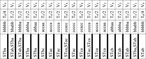
Table 2. Space vector switching sequence execution with commutation representation.
6. Maximum modulation index and voltage gain formulation in N to K phase QZSDMC
The voltage gain of the QZSDMC is given by G = BM, where G is the voltage gain of QZSDMC, B is the boost factor for QZSDMC and M is the modulation index for QZSDMC. Table shows the maximum modulation index formulation for N to K phase QZSDMC. The maximum output in the linear range can be getting for N to K phase QZSDMC as
(22)
(22)
(23)
(23)
Table 3. Maximum modulation index and voltage gain formulation.
7. Simulation results and discussions
The simulation work is supported to study the operation and performance of this converter in the whole range of operations. The suggested modulation scheme for QZSDMC provides excellent performance in all the operating regions. The MATLAB/Simulink platform is used to develop the simulation model by using the library block of the simpowersystem.
The block diagram representation of the suggested PWM is presented in Figure . The MatLab/Simulink environment is used to validate the proposed dual space vector PWM for QZSDMC. Also, the viability of the design is checked by constructing the experimental prototype. Table represents the parameters chosen for various elements used in simulation and real-time hardware equipment. In the simulation part, the QZSDMC waveforms are validated by comparing them with normal DMC waveforms. Figure (b) shows the input phase voltages with a magnitude of 100 V, 50 Hz frequency. Assume 0.66 as modulation index M0 and 0.34 as shoot-through duty ratio D0. Figure (a,b) shows the output five-phase voltages of 145 V (RMS) and 2.45 A load current. The calculated gain of QZSDMC is 2.05. This gain value represents the relationship between output voltages concerning input voltages, i.e. the output voltage is 2.05 times of input voltages with a cut-off frequency of 5 kHz.
Figure 7. Schematic representation of simulation set-up.
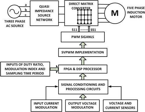
Figure 8. (a) Controlled switching signals generated by a dual SVPWM control technique for each leg. (b) Three-phase input voltages and current for 3φ to 5φ QZSDMC with frequency 50 Hz.
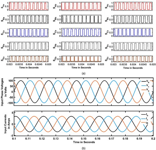
Figure 9. (a) Three-phase output phase voltages and line voltages at frequency 50 Hz. (b) Three-phase output load currents at frequency 50 Hz. (c) Output voltages THD of three-phase to three-phase QZSDMC. (d) Output current THD of three-phase to three-phase QZSDMC.
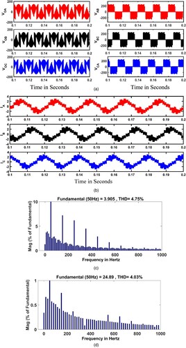
Table 4. MatLab simulation and experimental parameters consideration.
Theoretically, the boost factor B is calculated as 3.125 with a maximum voltage gain of 2.06. Using these parameters, the period for shoot-through duty ratio can be calculated as 0.34 which is the same as the theoretical value. The simulation results for the conventional DMC show the output phase voltages of 86.65 V (RMS). It represents the voltage transfer ratio of conventional DMC is only 0.866 which is less than the voltage transfer capability of QZSDMC. Also, the sinusoidal nature with continuous input current waveforms can be getting from QZSDMC. On the other side, the input current flows through the conventional DMC has pulsating current with higher harmonics voltage and current as shown in Figure (c,d).
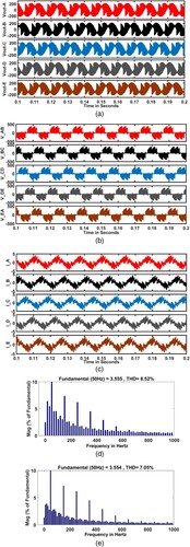
Figure shows the five-phase output voltage and current waveforms with harmonics representations getting from the 3φ to 5φ QZSDMC with the input voltages of 100 V peak at frequency 50 Hz. The 3φ to 5φ QZSDMC has the capability of producing various output voltages and frequencies like 25, 75 and 100 Hz. From Figures , the researcher can observe the inbuild wide range voltage gain capability of QZSDMCS with more than three phases. From the proposed converter, the following points are proven clearly. A wide range of voltage gain, sinusoidal nature of input current with less THD, minimum usage of power switches compared with back-to-back connected multiphase voltage source inverter and the input filter elimination. As per the control law, the output pattern for controlling the output voltage is directly derived and these control signals are given to the switches as shown in Figure (a).
Figure 10. (a) Five-phase output phase voltages at frequency 50 Hz. (b) Five-phase output line voltages at frequency 50 Hz. (c) Five-phase load currents at frequency 50 Hz. (d) Output voltages THD of three-phase to five-phase QZSDMC. (e) Output current THD of three-phase to five-phase QZSDMC.
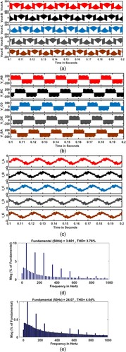
Figure 11. (a) Three-phase output phase voltages and line voltages at frequency 25 Hz. (b) Three-phase output load currents at frequency 25 Hz. (c) Output voltages THD of three-phase to three-phase QZSDMC. (d) Output current THD of three-phase to three-phase QZSDMC.
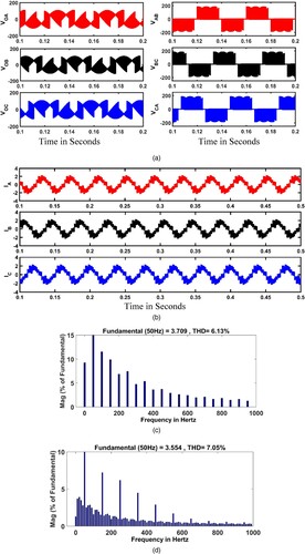
Figure 12. (a) Five-phase output phase voltages at frequency 25 Hz. (b) Five-phase output line voltages at frequency 25 Hz. (c) Five-phase output load currents at frequency 25 Hz. (d) Output voltages THD of three-phase to five-phase QZSDMC. (e) Output current THD of three-phase to five-phase QZSDMC.
Figures show the voltage THD and current THD of conventional DMC and 3φ to 5φ QZSDMC. From that Figures , the observation taken as THD of 3φ to 5φ QZSDMC is less than the THD of conventional DMC by the percentage of 2.5. The voltage THD and current THD of 3φ to 5φ QZSDMC are 3.76 and 4.04%, respectively, and the voltage THD and current THD of conventional DMC are 4.76 and 4.03%, respectively, with a frequency 50 Hz. These THD tolerance limits are specified within the IEEE19-1999 standards. Table shows the consolidated observation getting from Figures like input voltage, output phase voltages, output line voltages, load currents, voltage harmonics and current harmonics of both three-phase output, and five-phase output of dual SVPWM-based QZSDMC with 25, 50, 75 and 100 Hz.
Table 5. Output parameters of dual SVPWM-based QZSDMC with different frequencies.
The proposed experimental prototype set-up structure is shown in Figure . The experimental results are used to validate the proposed concepts of the dual space vector PWM technique for 3φ to 5φ QZSDMC. These experimental results are helpful to analyse and justify the theoretical concepts, reliability, and ease of digital implementation. Hence, the proposed direct ac–ac converter can be used for the wide range of speed control for multiphase drive systems. The schematic blocks for the experimental set-up are as shown in Figure . Figure represents the experimental set-up of a three-phase to five-phase quasi Z-source direct matrix converter. The IXYS-based FIO50-12BD bidirectional switches-based power modules are used to compose the required experimental prototype set-up. It’s an ISOPLUS i4-PAC consisting of fast diode bridges and diagonally connected IGBTs. The IGBTs and diode bridges have the voltage blocking capability of 1200 V and the current-carrying capability of each device are 50 A.
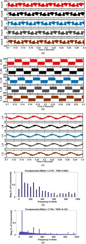
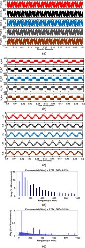
Figure 13. (a) Three-phase output phase voltages and line voltages at frequency 75 Hz. (b) Three-phase output load currents at frequency 75 Hz. (c) Output voltages THD of three-phase to three-phase QZSDMC.(d) Output current THD of three-phase to three-phase QZSDMC.
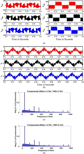
Figure 14. (a) Five-phase output phase voltages at frequency 75 Hz. (b) Five-phase output line voltages at frequency 75 Hz. (c) Five-phase output load currents at frequency 75 Hz. (d) Output voltages THD of three-phase to five-phase QZSDMC. (e) Output current THD of three-phase to five-phase QZSDMC.
This module is available in the market as a single chip with five output pins. Among the five output pins, four pins are used to diode bridges, and one pin is used to IGBT gate drive circuit. Using the single control signal, the bidirectional current flow can be controlled by a single chip module. The QZSDMC consists of 27 bidirectional power switches among that 18 switches are effectively utilized. The spartan 3-A DSP controller and Xilinx XC3SD1800A FPGA are used to generate the control signals for bidirectional switching devices. The FPGA board consists of logic gates, A/D and D/A conversion processors, gate drive signal generator and modulation code processor. The FPGA board has the capability of handling the PWM signals up to 50. The entire power module circuit is protected using damping diode circuits.
The autotransformer is used to provide the input power supply of 100 V, 50 Hz, 3phase AC power. The QZSDMC is made of bidirectional switches with a switching frequency of 5 kHz. Table represents various input side parameters, filter parameters and output side load parameters. Figure (a) shows 3φ to 5φ QZSDMC resulting output per phase voltage waveforms with the fundamental frequency of 25, 50, 75 and 100 Hz. Figure (b) shows 3φ to 5φ QZSDMC resulting output per line voltage waveforms with the fundamental frequency of 25, 50, 75 and 100 Hz. Figure (c) shows the resulting output per phase current waveforms with the fundamental frequency of 25, 50, 75 and 100 Hz. Figure (d) shows 3φ to 5φ QZSDMC experimental output voltage of 145 V (RMS) with the operating frequency of 25, 50, 75 and 100 Hz. In general, Figure shows 3φ to 5φ QZSDMC experimental sample output phase voltage, line voltage, load current of 3.3 A with the operating frequency of 25, 50, 75 and 100 Hz. Referring to Figure , the output voltage and output current of conventional DMC are limited to 86.667 V (RMS) and 2.8 A. From the experimental results, the observation is taken as voltage gain of 3φ to 5φ QZSDMC is superior to the conventional DMC. The reason behind the increased voltage gain of 3φ to 5φ QZSDMC is the distribution of shoot-through states evenly without changing the active states. Figure shows the output phase voltage waveforms are adjusted in-phase with the output load currents. It means the unity power factor is maintained at the load side.
Figure 15. (a) Three-phase output phase voltages and line voltages at frequency 100 Hz. (b) Three-phase output load currents at frequency 100 Hz. (c) Output voltages THD of three-phase to three-phase QZSDMC. (d) Output current THD of three-phase to three-phase QZSDMC.
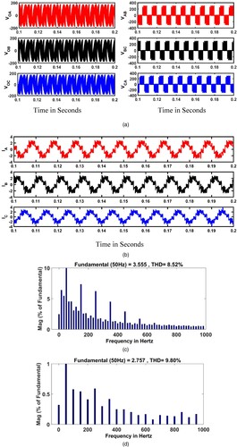
Figure 16. (a) Five-phase output phase voltages at frequency 100 Hz. (b) Five-phase output line voltages at frequency 100 Hz. (c) Five-phase output load currents at frequency 100 Hz. (d) Output voltages THD of three-phase to five-phase QZSDMC. (e) Output current THD of three-phase to five-phase QZSDMC.
Thus, the dual space vector control and modulation algorithm-based QZSDMC hardware results validate its performance better than the conventional DMC. Figure represents the step-by-step procedure of experimental validation in a flowchart form. The implementation of a dual SVPWM control scheme for 3φ to 5φ QZSDMC was represented clearly. Table shows the comparative evaluation of simulated results with the experimental prototype results. Most of the measured results are equating to the theoretical results via simulation. The main constraints followed in the experimental set-up are non-ideal parameters of inductors and capacitors. As a result, unpredicted voltage drops arise across the power devices and inductors. So the expected voltages of the QZS network are less than the simulated output voltages.
Table 6. Comparison between simulation and experiment results of QZSDMC.
The experimental results mostly coincide with the simulation results to a good extent. Figures show an input voltage and current THDs with output voltage and current THDs. The output voltage and current THDs of 3φ to 5φ QZSDMC are 3.76 and 4.04%, respectively. The three-phase input voltage and current THDs are 4.76 and 4.03%, respectively. This result shows the superior performance of 3φ to 5φ QZSDMC with the proposed dual space vector PWM technique. Further at the input side, the current is in phase with the voltage waveforms. The beauty of the proposed converter is prooved by maintaining the unity power factor at the input side.
The prototype module uses bidirectional switches. The major advantage is the utilization of a minimum number of IGBT switches for multiphase operation. The considerable disadvantages are higher conduction losses, two-step commutation, usage of extra line inductance for safe operation, overlapping of current during commutation, and the requirement of clipping circuits and snubbers for dead time compensations. The testing of developed QZSDMC is done over a wide range of fundamental frequencies.
Figure 17. Structure of experimental prototype set-up experimental results and discussions.
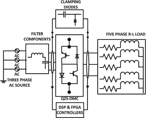
Figure 18. Experimental set-up of a three-phase to five-phase quasi Z-source direct matrix converter.
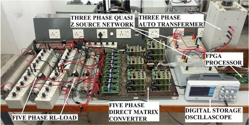
Figure 19. Experimental per phase result of a three-phase to five-phase quasi Z-source direct matrix converter.
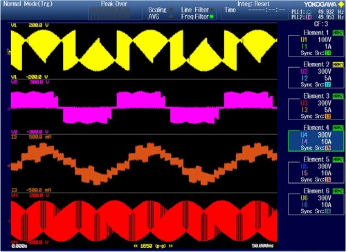
Figure 20. Flowchart for experimental validation of control scheme employed in QZSDMC.
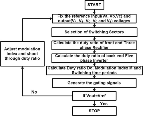
Figure 21. Experimental input current THD of 4.03%.

Figure 22. Experimental input voltage THD of 4.76%.
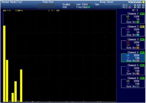
Figure 23. Experimental output voltage THD of 3.76%.
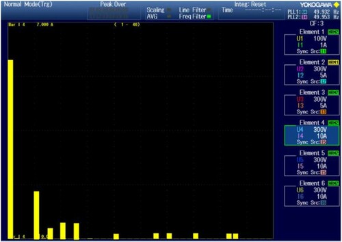
Figure 24. Experimental output current THD of 4.04%.
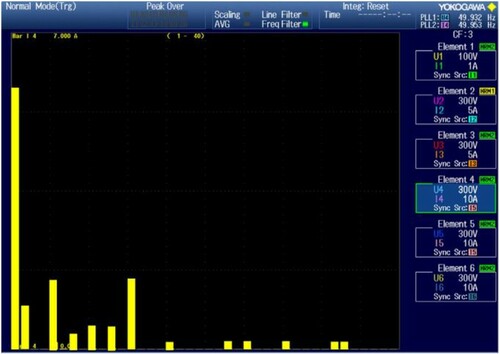
Table shows the comparison of ZSDMC, discontinuous and continuous QZSDMC AC–AC converter topologies. From the comparison, it is ensured that the QZSDMC offers a high voltage boost ratio, good waveform quality, lesser capacitor voltage stress and continuous input current. The simulation and the investigational results of the prototype verify the feasibility of the suggested QZSDMC topology and its control strategy. Comparing the hardware results with the simulation results, that show the proposed modulation scheme for QZSDMC provides better results at all the fundamental frequencies.
Table 7. Quantitative comparison of direct and indirect QZSDMC with discontinuous and continuous mode operations.
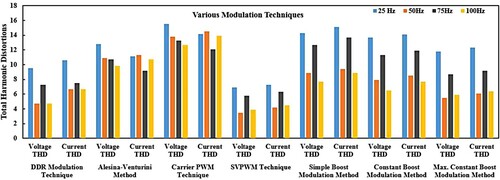
Table shows the comparison of direct duty ratio PWM technique with various classic modulation techniques like Alesina-Venturini modulation technique, Carrier PWM Technique, SVPWM Technique, Simple Boost Modulation Method, Constant Boost Modulation Method and Maximum Constant Boost Modulation Method. This comparison is based on the current and voltage THD getting from each method at different operating frequencies of the QZSDMC. At the operating frequency = 25 Hz, the SVPWM technique-based QZSDMC generated the voltage and current harmonic distortion of 6.9 and 7.3%, respectively. Whereas the DDR-based PWM technique generates the voltage and current harmonic distortion of 9.52 and 10.62%, respectively. The remaining modulation techniques are producing more THD in the mentioned operating frequency. At the operating frequency = 50 Hz, the SVPWM technique-based QZSDMC generating the voltage and current harmonic distortion of 3.5 and 4.2%, respectively. Whereas the DDR-based PWM technique generates the voltage and current harmonic distortion of 4.7 and 6.7%, respectively. The remaining modulation techniques are producing more THD in the mentioned operating frequency [Citation55].
Table 8. Comparison of THD generation by various modulation techniques.
At the operating frequency = 75 Hz, the SVPWM technique-based QZSDMC generated the voltage and current harmonic distortion of 5.8 and 6.3%, respectively. Whereas the DDR-based PWM technique generates the voltage and current harmonic distortion of 7.3 and 7.5%, respectively. The remaining modulation techniques are producing more THD in the mentioned operating frequency. At the operating frequency = 100 Hz, the SVPWM technique-based QZSDMC generates the voltage and current harmonic distortion of 3.9 and 4.5%, respectively. Whereas the DDR-based PWM technique generates the voltage and current harmonic distortion of 4.7 and 6.7%, respectively. The remaining modulation techniques are producing more THD in the mentioned operating frequency.
The comparison represented in Figure represents the performance of each technique implemented in ZSDMC concerning its voltage and current THD values. The comparison figure shows that the proposed modulation technique is better than the classic modulation techniques which are prosed to the various Z-source matrix converter [Citation55].
Figure 25. Comparison of voltage THD and current THD generation by QZSDMC for various classic PWM techniques.
8. Conclusion
In this paper, the dual space vector pulse width modulation control technique was proposed to three-phase to five-phase QZSDMC. Here, the input is three-phase, while the output is five-phase. A five-phase motor drive application can effectively utilize this type of converter. In the proposed dual SVPWM technique, 93 active space vectors are utilized from the possible 243 switching space vectors. For one sampling period, utilization of active vectors, zero vectors, 24 commutations and symmetrical switching of each half period is obtained. The proposed QZSDMC topology was consisting of a three-phase QZS network with five-phase DMC. The restrictions of voltage transfer ratio in the conventional DMC were overcome by 3φ to 5φ QZSDMC. In this paper, the proposed dual SVPWM technique was discussed in detail. The limitation associated with the conventional DMC at linear modulation is voltage gain. The attained voltage boost capability of the proposed QZSDMC is 1.97. In the absence of extra input filters, the voltage gain attainment is greater than unity. The experimental prototype set-up was fabricated to verify the simulation results. Both results are investigated and justified in detail. The simulation and hardware results show the maximum boost output voltage of 145 V (RMS) with a voltage gain of 1.97 and a shoot-through duty ratio of 0.33. By doing a comparison between 3φ to 5φ QZSDMC with conventional DMC, the voltage transfer capability was observed as 1.97 and 0.8667, respectively. The major advantages of the proposed converter are continuous input and output currents during any phase fault, nearly unity power factor at both sides, absence of bulky input LC filters and low input current THD as well as low output voltage THD. In the motor drive applications and the renewable energy applications, the occupation of conventional DMC can be replaced by the proposed 3φ to 5φ QZSDMC with its promising dual space vector PWM control technology. In the future, the performance of the proposed converter under the over modulation region in the SVPWM technique can investigate, the effects of fault tolerance, stability and performance variation during any one phase fault condition can analyse, the performance of proposed modulation schemes for multiphase to three-phase energy conversion systems applied for wind energy systems can investigate, a quasi-impedance source-based multiphase multilevel matrix converter for changing the energy capture and improve the performance of wind energy conversion systems can develop, this converter topology in wind energy conversion system to maintain constant voltages and frequency at load side from continuous variations in the wind speeds can apply, different topologies with improved impedance source network such as T-network could be used to multiphase QZSDMC and the performance evaluation of multiphase motor drive fed by multiphase matrix converter with the proposed control algorithm can evaluate. These are all wide range of areas for the proposed matrix converter can work for better future extraction.
Disclosure statement
No potential conflict of interest was reported by the author(s).
REFERENCES
- Iqbal S, Ahmed M, Abu-Rub H. Space vector PWM technique for a three-to-five-phase matrix converter. IEEE Trans Ind Appl. 2012;48(2):697–707. DOI:https://doi.org/10.1109/TIA.2011.2181469.
- Pipolo S, Formentini A, Trentin A, et al. A novel matrix converter modulation with a reduced number of commutations. IEEE Trans Ind Appl. 2021;57(5):Sept.-Oct. 2021.
- Thangavel MK, Ramasamy BK, Ponnusamy P. Performance analysis of dual space vector modulation technique-based quasi Z-source direct matrix converter. Electr Power Components Syst. 2020;48(11):1–12.
- Chitra & K, Jeevanandham A. High-efficient three-phase on-line UPS by using T-source inverter with third harmonic injected maximum constant boost PWM control. J Chin Inst Eng. 2016;39(2):139–149. DOI:https://doi.org/10.1080/02533839.2015.1082935.
- Chitra K. Modeling and simulation of trans Z-source inverter with maximum constant boost PWM control for solar PV system. Singapore: Intelligent Manufacturing and Energy Sustainability, Springer; 2020.p. 663–673.
- Ahmed SM, Iqbal A, Abu-Rub H, et al. Vector control of a five-phase induction motor supplied by a Non-square 3X5 phase matrix converter. Aust J Electr Electron Eng. 2013;10(1):55–63.
- Chitra K, Prakash VS, Kamatchi KV, et al. Implementation of simple boost PWM controlled T-source inverter for solar PV application. Int J Sci Technol Res. 2019;8(11):717–720.
- Tawfiq KB, Ibrahim MN, EL-Kholy EE, et al. (2021). Performance analysis of a five-phase synchronous reluctance motor connected to matrix converter. In 2021 IEEE International Electric Machines & Drives Conference (IEMDC), p. 1–6.
- Malekjamshidi Z, Jafari M, Zhu J, et al. Bidirectional power flow control with stability analysis of the matrix converter for microgrid applications. Int J Electr Power Energy Syst. 2019;110:725–736.
- Chitra K, Prakash VS. Analytical comparison and implementation of different inverter topologies for three-phase on-line uninterruptible power supply. Int J Ambient Energy. 2019;43(1):1103–1112. doi:https://doi.org/10.1080/01430750.2019.1688678.
- Siwek P, Urbanski K. Improvement of the torque control dynamics of the PMSM drive using the FOC-controlled simple boost QZSDMC converter. In 23rd Int. Conf. Methods Model. Autom. Robot. MMAR 2018; 2018.p. 29–34.
- Guo M, Liu Y, Ge B, et al. Optimum boost control of quasi-Z source indirect matrix converter. IEEE Trans Ind Electron. 2018;65(10):8393–8404.
- Iqbal A, Khan MA, Ahmed SM, et al. Analysis of discontinuous space vector PWM techniques for a five-phase voltage source inverter. Int J Recent Trends Eng. 2009;2(5):222.
- Sayed MA, Iqbal A. Pulse width modulation technique for a three-to-five phase matrix converter with reduced commutations. IET Power Electron. 2016;9(3):466–475.
- Moghadasi N, Esmaeli A, Soleymani S, et al. Quasi-Z-source matrix converters to be used in PMSG-based WECS: modeling, control, and comparison. Int Trans Electr Energy Syst. 2018;28(6):1–27.
- Bozorgi AM, Hakemi A, Farasat M, et al. Modulation techniques for common-mode voltage reduction in the Z-source ultra sparse matrix converters. IEEE Trans Power Electron. 2018;34(1):958–970.
- Ahmed SM, Salam Z, Abu-Rub H. An improved space vector modulation for a three-to-seven-phase matrix converter with a reduced number of switching vectors. IEEE Trans Ind Electron. 2014;62(6):3327–3337.
- Guo M, Liu Y, Ge B, et al. Optimum boost control of quasi-Z source indirect matrix converter. IEEE Trans Ind Electron. 2018;65(10):8393–8404.
- Sri Vidhya D, Venkatesan T. Quasi-Z-source indirect matrix converter fed induction motor drive for flow control of dye in paper mill. IEEE Trans Power Electron. 2018;33(2):1476–1486.
- Li X, Sun Y, Zhang J, et al. Modulation methods for indirect matrix converter extending the input reactive power range. IEEE Trans Power Electron. 2017;32(6):4852–4863.
- Savrun MM, Atay A. The novel multiport bidirectional DC-DC converter for PV powered electric vehicle equipped with battery and supercapacitor. IET Power Electron; 13(17):3931–3939. doi:https://doi.org/10.1049/iet-pel.2020.0759.
- Savrun MM. “Z-source converter integrated dc electric spring for power quality improvement in dc microgrid. Eng Sci Technol. 2021;24(6):1408–1414.
- Ayten K, Savrun MM. Coupled inductor based quasi-Z source converter integrated three-level boost converter with reduced input current ripple. International Arslantepe Scientific Research Congress.
- Alizadeh M, Kojori SS. Small-signal stability analysis, and predictive control of Z-source matrix converter feeding a PMSG-WECS. Int J Electr Power Energy Syst. 2018;95:601–616.
- Khan MA, Iqbal A, Ahmad SM. Space vector pulse width modulation scheme for a seven-phase voltage source inverter. Int J Power Electron Drive Syst. 2011;1(1):7.
- Moinuddin S, Iqbal A, Abu-Rub H, et al. Three-phase to seven-phase power converting transformer. IEEE Trans Energy Convers. 2012;27(3):757–766.
- Khan MA, Iqbal A, Ahmad SM, et al. Analysis of discontinuous space vector PWM techniques for a seven-phase voltage source inverter. Int J Power Electron Drive Syst. 2012;2(2):203.
- Liu Y, Ge B, Abu-Rub H, et al. Single-phase Z-source/quasi-Z-source inverters and converters. IEEE Ind Electron Mag. 2018;12(2):6–23.
- Liu Y, Liang W, Ge B, et al. Quasi-Z-source three-to-single-phase matrix converter and ripple power compensation based on model predictive control. IEEE Trans Ind Electron. 2018;65(6):5146–5156.
- Dabour SM, Abdel-Khalik AS, Ahmed S, et al. Common-mode voltage reduction for space vector modulated three- to five-phase indirect matrix converter. Int J Electr Power Energy Syst. 2018;95:266–274.
- Moinuddin S, Abu-Rub H, Iqbal A, et al. Space vector pulse-width modulation technique for an eleven-phase voltage source inverter with sinusoidal output voltage generation. IET Power Electron. 2015;8(6):1000–1008. DOI:https://doi.org/10.1049/iet-pel.2014.0327.
- Ahmed SM, Abu-Rub H, Salam Z. Common-mode voltage elimination in a three-to-five-phase dual matrix converter feeding a five-phase open-end drive using space-vector modulation technique. IEEE Trans Ind Electron. 2015;62(10):6051–6063. DOI:https://doi.org/10.1109/TIE.2015.2420038.
- Saleh M, Khan MA, Iqbal A, et al. Three-to-seven phase matrix converter supplied seven-phase three-motor drive system. J Innov Electron Commun Eng. 2013;3(2):6–13.
- Ahmed SM, Abu-Rub H, Iqbal A. Pulse width modulation control of a direct AC-AC power converter with five-phase input and three-phase output. Int J Autom Power Eng. 2012;1(8):186–192.
- Zhou M, Sun Y, Su M, et al. A single-phase buck-boost AC-AC converter with three legs. J Electr Eng Technol. 2018;13(2):838–848.
- Saeed N, Ibrar A, Saeed A. A review on industrial applications of Z-source inverter. J Power Energy Eng. 2017;05(09):14–31.
- Li M, Liu Y, Abu-Rub H. Optimizing control strategy of quasi-Z source indirect matrix converter for induction motor drives. IEEE Int Symp Ind Electron. 2017;(DMC):1663–1668.
- Hakemi A, Monfared M. Very high gain three-phase indirect matrix converter with two Z-source networks in its structure. IET Renew Power Gener. 2017;11(5):633–641.
- Alizadeh M, Kojori SS. Modified predictive control for both normal and LVRT operations of a quasi-Z-source matrix converter based WECS. Control Eng Pract. 2017;68:1–14.
- Ellabban O, Abu-Rub H, Bayhan S. Z-source matrix converter: an overview. IEEE Trans Power Electron. 2016;31(11):7436–7450.
- Pinto SF, Mendes PV, Fernando Silva J. Modular matrix converter based solid state transformer for smart grids. Electr Power Syst Res. Jul. 2016;136:189–200.
- Liu S, Ge B, Liu Y, et al. Modeling, analysis, and parameters design of LC-filter-integrated quasi-Z-source indirect matrix converter. IEEE Trans Power Electron. 2016;31(11):7544–7555.
- Liu S, Ge B, You X, et al. A novel quasi-Z-source indirect matrix converter. Int J Circuit Theory Appl. 2015;43(4):438–454.
- Moin Ahmed SK, Abu-Rub H, Iqbal A. Multiphase matrix converter topologies and control. Power Electron Renew Energy Syst Transp Ind Appl. 2014;9781118634:463–502. DOI:https://doi.org/10.1002/9781118755525.ch15.
- Ellabban O, Abu-Rub H, Ge B. A quasi-Z-source direct matrix converter feeding a vector controlled induction motor drive. IEEE J Emerg Sel Top Power Electron. 2015;3(2):339–348.
- Takahashi N, Liu S, Ge B, et al. Modeling, analysis, and motor drive application of quasi-Z-source indirect matrix converter. COMPEL Int J Comput Math Electr Electron Eng. 2014;33(1-2):298–319.
- Empringham L, Kolar JW, Rodriguez J, et al. Technological issues and industrial application of matrix converters: a review. IEEE Trans Ind Electron. 2013;60(10):4260–4271.
- Liu S, Ge B, Jiang X, et al. Comparative evaluation of three Z-source/quasi-Z-source indirect matrix converters. IEEE Trans Ind Electron. 2014;62(2):692–701.
- He L, Duan S, Peng F. Safe-commutation strategy for the novel family of quasi-Z-source AC–AC converter. IEEE Trans Ind Informatics. 2013;9(3):1538–1547.
- Friedli T, Kolar JW, Rodriguez J, et al. Comparative evaluation of three-phase AC–AC matrix converter and voltage DC-link back-to-back converter systems. IEEE Trans Ind Electron. 2012;59(12):4487–4510.
- Nguyen M, Lim Y, Kim Y. A modified single-phase quasi-Z-source AC–AC converter. IEEE Trans Power Electron. 2012;27(1):201–210.
- Bharani Kumar R, Adhisree VV, Nirmal Kumar A. Performance analysis of Z-source matrix converter by implementing different PWM schemes. J Electr Eng. 2012;12(3):193–201.
- Liu X, Loh PC, Wang P, et al. Improved modulation schemes for indirect Z-source matrix converter with sinusoidal input and output waveforms. IEEE Trans Power Electron. 2012;27(9):4039–4050.
- Perez MA, Rojas CA, Rodriguez J, et al. A simple modulation scheme for a three-phase direct matrix converter. IEEE Int Symp Ind Electron. 2012:105–110.
- Manivannan S, Saravanakumar N, Vijeyakumar KN. Three-phase power conversion using quasi Z source direct matrix converter (QZSDMC) for fixed frequency to variable frequency using direct duty ratio based pulse width modulation technique. Int J Electron. 2021. DOI:https://doi.org/10.1080/00207217.2021.1966668.