
 ?Mathematical formulae have been encoded as MathML and are displayed in this HTML version using MathJax in order to improve their display. Uncheck the box to turn MathJax off. This feature requires Javascript. Click on a formula to zoom.
ABSTRACT
The paper proposes an efficient DC-DC converter for renewable energy applications. The proposed high-gain converter is designed with switched inductor cell and voltage multiplier cell. In the proposed converter, the continuous source current is obtained by switched inductor cells, and high-voltage gain is achieved using voltage multiplier cells. The proposed converter provides a voltage gain of 10 when operated with a duty ratio of 27.3%, whereas a voltage gain of 39 is obtained for an 80% duty ratio. The efficiency of 96.54% is achieved in simulation for the rated condition of 24 V/240 V, 120W. The converter operation under steady-state, state-space modelling, and voltage and current stress of the power semiconductor components are analyzed. In addition to that, loss distribution and efficiency analysis are made. The performance of the converter is analyzed using the Matlab Simulink tool. Also, the experimental hardware prototype model is developed to validate the simulated and theoretical analysis.
1. Introduction
The power conversion systems require high-gain DC-DC boost converters. This requirement has increased due to applications of higher efficiency and power density. DC-DC boost converters are used in various applications, including battery charging in uninterruptible power supplies, electric vehicles, and DC distribution systems, since these applications require high-voltage gain converters. The source voltage is increased to match the load's requirements using a DC-DC boost converter. High-performance DC-DC converters have gained significant popularity due to their use in photovoltaic (PV) applications. For DC distributed generation systems, solar photovoltaic is one of the essential energy sources. Based on the system requirement, the converter topologies have been chosen. The selection criteria include switching mechanisms, directions of power flow, type of isolation, voltage/current supplied and system stability. In [Citation1], the converter is designed using passive switched capacitors. Although using a large number of switched capacitors increases gain, it also increases the input current's ripple. In paper [Citation2], the authors focus on a hybrid converter with one switch, one inductor, and several capacitors. The boost structure of the converter provides regulating capability, while the voltage multiplier structure provides gain improvement. In [Citation3], a boost converter with an active switched inductor is proposed. The circuit has low voltage stress across the diode, constant input current and a lower rating of voltages for passive components. It has a gain of 4/(1-D). The main reason for the variations in the theoretical and experimental gain is the parasitic internal resistance of several circuit components. It causes a decline in the converter's efficiency. In [Citation4], the author briefs about a high-gain converter that uses regenerative boost configuration. The gain obtained is (2-D) / (1-D)². A non-isolated non-coupled inductor-based topology for DC microgrids is suggested in [Citation5]. This converter provides a gain of (D2-3D + 3)/(1-D)². The main downside of converter architecture is pulsating output current and relatively high switch current stress. A converter consisting of a high-conversion-ratio interleaved boost stage and multiplier circuit is proposed in [Citation6]. The voltage multiplier cell present in the converter provides a high conversion ratio. It provides a gain of 4/(1-D). In the paper [Citation7], the authors describe a transformerless boost-based DC-DC converter. The components’ normalized peak voltage stress can also be greatly lowered by increasing the number of interleaving stages. The gain of this converter is (2 + 4D)/(1-D). A unique quadratic buck–boost converter is presented in [Citation8]. An interleaved boost type converter is presented in [Citation9]. A coupled inductor with switching capacitors provides a very high-gain. This type of converter is better suited to boost low output voltages. The paper [Citation10] suggests a high step-up transformerless DC-DC converter. The efficiency of this topology is 93% and provides a voltage gain of up to 10 times the input voltage. Various VMCs are used in [Citation11] to improve the gain of interleaved converters. Using more switched capacitors boosts the converter's gain and increases the incoming current's ripple. In the paper [Citation12], the authors describe a non-isolated topology. This design, however, necessitates a larger number of inductors. In [Citation13], a switched capacitor structure is used. However, this structure must be utilized with other DC-DC converters to regulate variable voltage. In [Citation14], the author discusses the DC-DC buck–boost converter. This converter has many switches, which would lead to high switching losses. In [Citation15], authors suggest that increasing the cascaded conventional boost converters can enhance gain. However, the components are subjected to a tremendous amount of voltage stress. Quadratic gain converters can also enhance the output voltage at lower duty cycles. In addition, as the duty cycle increases, the current increases, resulting in larger converter losses. There is a large voltage gain and less component voltage stress [Citation16]; however, the input and output of these circuits are not connected to the same ground. Voltage sampling will become more difficult as a result of this. These issues hamper the implementation of topology. In [Citation17], the authors categorize the topologies into two groups depending on whether or not a transformer is employed. In general, isolation transformers significantly benefit from obtaining a high-gain. The disadvantage is that using such transformers increases the converter's cost and size. At lower duty cycles, quadratic gain converters can increase the output voltage. In [Citation18], a quadratic buck–boost converter is proposed. These converters employ many switching capacitors cells to achieve high-gain without using coupled inductors and transformers. The disadvantage is that there will be high converter losses when the duty cycle increases. A transformerless DC-DC converter is discussed in [Citation19]. This converter has lesser gain and more stress when compared to the converter proposed. In [Citation20], the authors present a non-inverting DC-DC converter. It generates a bigger voltage gain while putting less strain on the switches. The suggested converter has a symmetrical configuration, so choosing the components is easier. The gain of the converter is (3 + D)/(1-D). In paper [Citation21], active switched inductor based boost converter topology is developed. Three power switches operated with two duty ratio is used to achieve high-voltage gain. The switched inductor and switched capacitor based boost converter topology is developed and its operating strategies are explained in [Citation22]. The coupled inductor and diode capacitor multiplier cell based boost converter structure is presented in [Citation23]. This study presents a new high-gain converter to solve these shortcomings. It has two symmetrical voltage multiplier cells and a three-diode gain cell. Compared to other existing converters, it has a better gain and efficiency. The components are easier to choose because the proposed converter has a symmetrical structure.
2. Proposed converter
Figure provides the circuit schematic for the proposed high-gain DC-DC converter. The converter's gain is increased by using two identical switched-inductor-based VMCs. Seven diodes D1 to D7, switches S1 and S2, five capacitors C1 to C5, and four inductors L1 to L4 make up the converter topology. S1 and S2 are operated using the same signal and simultaneously turned on and off. The converter operates in two modes based on the gating signal and is shown in Figure .
Figure 1. Proposed high-gain DC-DC converter.
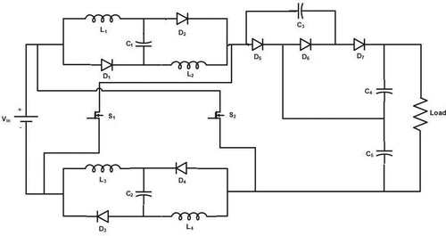
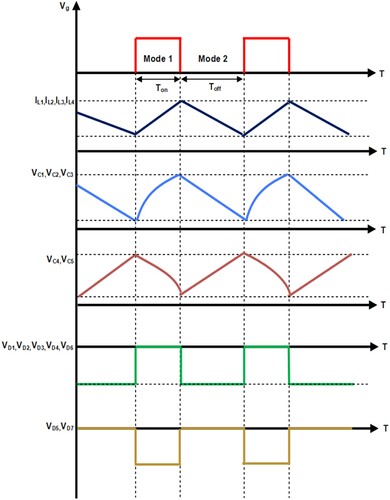
Figure 2. Switching waveform.
2.1. First mode of operation
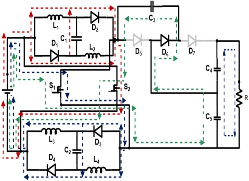
During Ton period, S1 and S2, diodes D1 to D4 and D6 are in forward bias while diodes D5 and D7 are in reverse bias. Also, capacitors C1, C2 and C3 are charging while other capacitors C4 and C5, are discharging. The diagram corresponding to the mode one operation is given in Figure .
Figure 3. First mode of operation.
The voltage expression for the inductors and capacitor current expression in first mode is obtained by applying KVL & KCL in Figure , and the Equations are represented as (1) to (8).
(1)
(1)
(2)
(2)
(3)
(3)
(4)
(4)
(5)
(5)
(6)
(6)
(7)
(7)
(8)
(8)
2.2. Second mode of operation
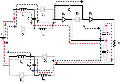
During Toff period, S1 and S2, diodes D1 to D4 and D6 are in reverse bias, diodes D5 and D7 operate and capacitors C4 and C5 are charging while other capacitors C1, C2, and C3 are discharging. The diagram corresponding to the second mode of operation is provided in Figure .
Figure 4. Second mode of operation.
The inductor voltage and capacitor current expression during second mode of operation is obtained from Figure , after applying KVL & KCL, the Equations are given as (9) and (14)
(9)
(9)
(10)
(10)
(11)
(11)
(12)
(12)
(13)
(13)
(14)
(14)
2.3. Voltage gain
By applying the volt–sec balance principle to Equations (1), (2), (9) and (10) the steady-state voltage gain expression of the proposed converter is given in Equation (18).
(15)
(15)
(16)
(16)
(17)
(17)
(18)
(18)
2.4. State space modelling
The generalized state space average behaviour of DC-DC converter over a period can be expressed as
(19)
(19)
(20)
(20)
where A = A1d + A2(1-d), B = B1d + B2(1-d), C =C1d + C2(1-d), D = D1d + D2(1-d) and d is duty cycle.
From Equations (1–8), the state space matrix for first mode of operation is given in Equations (21 & 22).
(21)
(21)
(22)
(22)
Similarly, the state space equations for the second mode of operation are obtained from Equations (9–14) and are given in Equations (23 and 24). The averaged state space equations of the proposed converter are derived from Equations (21–24) is expressed in Equations (25 and 26).
(23)
(23)
(24)
(24)
(25)
(25)
(26)
(26)
3. Design of passive component
3.1. Design of inductor
The inductor design of proposed converter is depends on input current ripple (ΔiL), switching frequency (fs) and duty ratio. The values for the inductors are designed from the Equations (27–31).
(27)
(27)
(28)
(28)
(29)
(29)
(30)
(30)
(31)
(31)
3.2. Selection of capacitor
The capacitor selection is based on switching frequency (fs), duty ratio (d), output current (I0), voltage ripple (ΔVC). The output capacitors C4 & C5 and capacitors C1, C2 and C3 are selected based on the equations (32–36)
(32)
(32)
(33)
(33)
(34)
(34)
(35)
(35)
(36)
(36)
3.3. Stress across the power semiconductor devices
Voltage stress and current stress of the power switches S1 and S2 in terms of output voltage and current during the first and second mode of operation is obtained and given in the equations (37 and 38).
(37)
(37)
(38)
(38)
The voltage across the power diodes and the average diode current in the converter is obtained from Figures and and given in equations (39–41)
(39)
(39)
(40)
(40)
(41)
(41)
The inductor current of the proposed converter is obtained by using the Equation (42).
(42)
(42)
3.4. Power loss calculation
The non-idealities of semiconductor devices are considered as a reason for power loss. The converter performance is verified by doing power loss manipulations. The inductor ripple current and capacitor ripple voltage is neglected to simplify the analysis. The losses in diodes, capacitors, switches, inductors are considered as power losses in DC-DC converters. The parasitic resistance in the inductors (rL), capacitors (rC), ON resistance of the diode (rd) and forward cut-in voltages (Vf) are considered for the power loss calculations. The power losses are calculated for the output power of 120 W, output voltage of 240 V, rd = 0.1Ω, rC = 0.08Ω, rC0 = 0.13Ω,Vf = 0.8V
3.4.1. Power loss in diode
In the proposed converter, power losses due to diodes is due to ON state resistance and forward cut-in voltage and are determined by using the equations (43–45).
(43)
(43)
(44)
(44)
(45)
(45)
(46)
(46)
3.4.2. Power loss in inductor
The power loss in the inductor is calculated by neglecting the ripple current and can be obtained by using the equations (47–49).
(47)
(47)
(48)
(48)
(49)
(49)
3.4.3. Power loss in capacitor
Neglecting the ripple voltage, the power loss in the capacitor is computed by using the equations (50–53).
(50)
(50)
(51)
(51)
(52)
(52)
(53)
(53)
3.4.4. Power loss in switch
The power losses in semiconductor switches are mainly due to conduction loss and switching loss. The switching loss is mainly due to turn on and turn off time. The ON-state resistance of the switch is responsible for conduction loss. The total loss in the switch is calculated by considering d = 0.273, rsw-on = 0.1Ω, ton = 23 ns, toff = 150 ns, fs = 20 kHz. The total power loss due to switches is obtained from the equation (54–56).
(54)
(54)
(55)
(55)
(56)
(56)
The total power loss of the proposed converter is given in Equation (57) and efficiency of the converter for the output power of 120W is calculated by using the Equation (59).
(57)
(57)
(58)
(58)
(59)
(59)
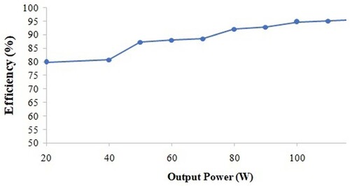
The distribution of power loss of the semiconductor devices are presented in the Figure . The maximum power loss occurs in power diodes followed by switches, capacitors and inductors. The efficiency of the proposed converter using the voltage gain and the total power loss is pictured in Figure . The converter attains the maximum of efficiency of 95.53% at the rated load power condition.
Figure 5. Power loss distribution curve.
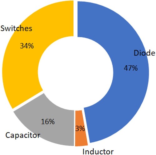
Figure 6. Efficiency against output power.
4. Comparative analysis
The comparative analysis of the proposed converter with the existing converter topology is discussed in this section. The voltage gain, voltage stress, current stresses of the devices, input ripple current are considered as a comparative metrics and are tabulated in Table . Figure depicts a voltage gain comparison of proposed converter with the other converters in the literature. The voltage gain of the proposed converter is 43.59% more than the gain obtained in [Citation1] for the duty ratio of 0.8. Though the number of components in the proposed converter is more when compared with the other converters, the duty ratio of 0.273 is sufficient to get the voltage gain of 10. The voltage stress of the proposed converter is 27% less than the converter in [Citation11]. One of the downside of the proposed converter is the high input current ripple.
Figure 7. Gain comparison with a duty cycle.
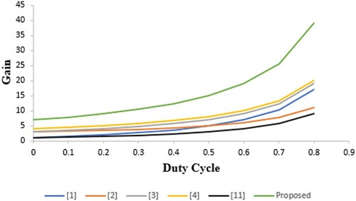
Table 1. Proposed converter comparison with the converters.
5. Simulation results of the proposed converter
The performance of the proposed converter is simulated using MATLAB simulink environment. The converter circuit parameters are calculated using the equations (30–36) and the values are tabulated in Table . The proposed converter is designed to maintain the output voltage of 240 V for the input voltage of 24 V. To maintain the constant output voltage, PI controller is employed. The controller parameters are tuned using Z-N method. The values of Kp and Ki are 0.01, 235 and 0.7687. The block diagram of PI controller is presented in Figure . The closed loop simulink model of proposed converter is shown in Figure .
Figure 8. Block diagram of PI controller.
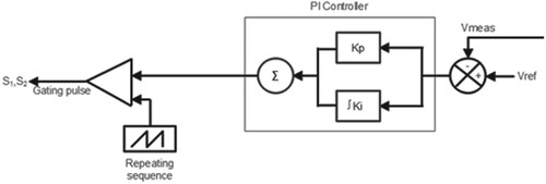
Figure 9. Closed Loop simulink model of proposed converter.
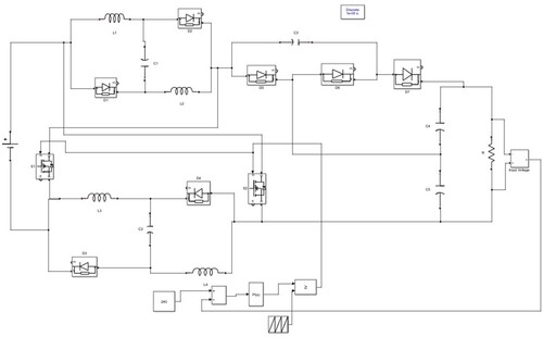
Table 2. Simulated parameters of proposed converter.
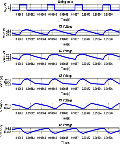
The resistive load is considered for converter performance analysis. The simulated voltage, current and power waveforms at the output of converter is shown in Figure . The PI controller employed in the converter regulates the output voltage and maintain at 240 V. Likewise, the inductor current waveforms are shown in Figure . When the switch is on, the inductors (L1, L2, L3, & L4) in the switched inductor cell get charged and dissipate its stored energy when the switch is off. The voltage waveforms of the capacitors in the switched inductor cell (C1, C2) and voltage multiplier cell (C3, C4, C5) are pictured in Figure .
Figure 10. Closed loop simulated output voltage, current and power waveforms.
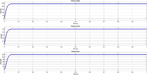
Figure 11. Simulated Inductor current waveforms.
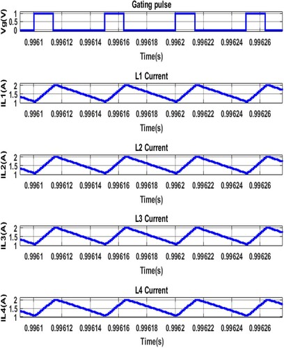
Figure 12. Simulated Capacitor Voltage waveforms.
The performance of the converter with the controller under transient condition is also be analyzed by varying the reference voltage, source voltage and load power.
5.1. Performance analysis of converter under line voltage variation
The line voltage of the converter is varied from 4 V above than the designed input voltage range and 4 V below the designed value. The line voltage is varied at different time intervals. At time t = 0, the line voltage is kept as 24 V, the converter maintains the load voltage of 240 V. At time t = 0.5s, the line voltage is reduced from 24 V to 20 V. The controller has to tracks the change in line voltage and generates the required gate signal to regulate the output voltage to 240 V. The controller takes less than .02s to regulate the output voltage. Likewise, at time t = 1s, the line voltage is varied from 20 V to 24 V. The controller takes the increase in line voltage variation and generates the gating pulse to maintain the output voltage. The voltage, current and power values at both input and output of the converter is noted during these variations and are tabulated in Table and the corresponding waveforms are depicted in Figure .
Figure 13. Simulated Line voltage regulation waveforms.
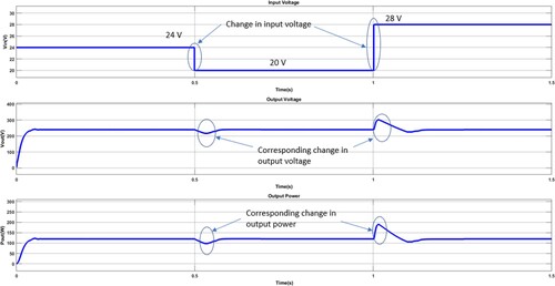
Table 3. Voltage, current and power values under line voltage variation.
5.2. Performance analysis of converter under reference voltage variation
The converter is designed to maintain the output voltage of 240 V. In this case, the controller’s ability is analyzed by varying the reference voltage of the converter. The reference voltage is varied at regular interval of time between 200 V to 280 V. At time t = 0s, the reference voltage is maintained at 240 V, the converter maintains this voltage at the output side. At time t = 0.5s, the reference voltage is made 40 V less that the initial value. The PI controller employed in the converter identifies the change in reference voltage and generates the gating signal to maintain the output voltage of 200 V. The change in reference voltage variations and the corresponding variations in output voltage and power are shown in Figure and the values are tabulated in Table .
Figure 14. Simulated Reference voltage variation waveforms.
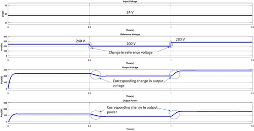
Table 4. Voltage, current and power values under the variation of reference voltage.
5.3. Performance analysis of converter under load power variation
In this case, the load power of the converter is varied from 40%, 60% and 100% of rated load condition. These variations are made at constant time intervals. The controller effectively tracks the change in load power variations and maintains the output voltage. The variation in change in load power and the corresponding variations in output voltage is given in Figure and the corresponding voltage, current and power values are tabulated in Table .
Figure 15. Simulated Load Power variation waveforms.
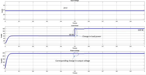
Table 5. Voltage, current and power values under load power variations.
6. Hardware implementation
In section 5, the converter performance is analysed in simulation environment. To validate the simulated results, hardware prototype type model is developed. The experimental model of the proposed converter is developed by considering the parameter values tabulated in Table . The hardware prototype model of the proposed converter is shown in Figure . The gate driver circuit generates the required gating signal for the converter switches. The prototype model is developed for the input voltage of 24 V, output voltage of 240 V and the power rating of 120W.
Figure 16. Hardware setup.
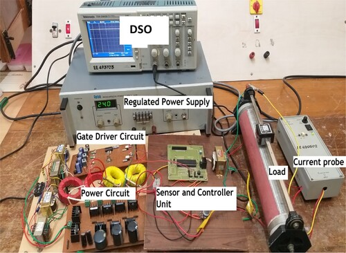
Table 6. Hardware specifications.
Figure 17. Gating pulse waveform.
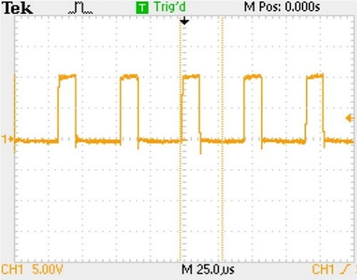
Figure 18. Output voltage Waveform for the source voltage of 24V.
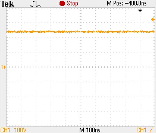
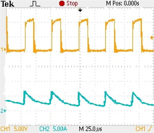
Figure 19. Line Voltage Regulation waveform under dynamic change in Input voltage from 20 V to 24V.
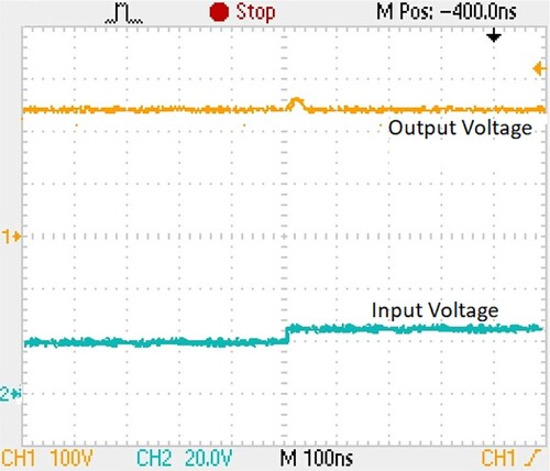
Figure 20. (a): Switch S1 Voltage Waveform. (b): Switch S2 voltage waveform.
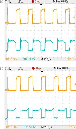
Figure 21. Inductor Current (IL1, IL2, IL3, IL4) Waveforms.
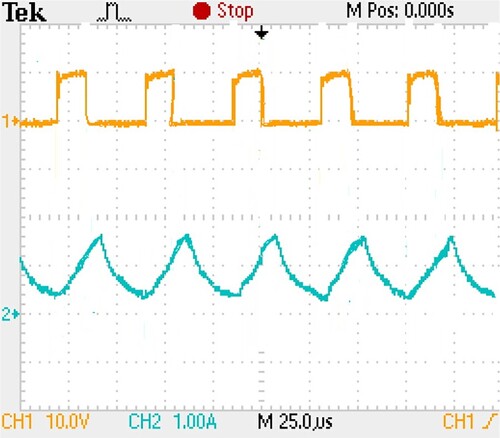
Figure 22. Diodes D1, D2, D3 voltage waveform.
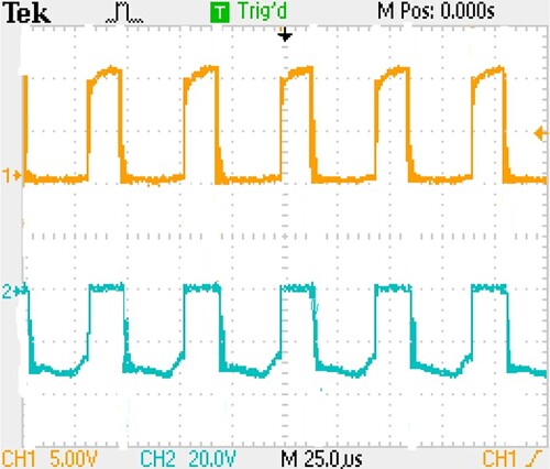
Based on the Equation (18), the output voltage of 240 V is attained for the source volatge of 24 V, duty ratio of 0.273. The gating signal required to achieve the required output voltage is generated using PIC microcontroller and the gate driver IC TL494. The gating pulse waveform is shown in Figure . The theoritical output voltage of 240 V is attained for the duty ratio of 0.273 while the output voltage of about 240 V is generated experimentally and shown in Figure . The result validaes the proposed converter attains the voltage gain of 10 at 0.273 duty ratio. Likewise, the transient behaviour of the converter with the controller is anlaysed experimentally by applying change in source voltage. Initially, the source voltage of 20 V is applied to the converter, the output voltage of 240 V is maintained and the source voltage is varied from from 20 V to 24 V, the controller tracks the change in voltage and ragulates the output voltage of 240 V and shown in Figure . In Figure (a,b) shows the voltage across the switches, S1 and S2. The theoritical value of voltage across the switch is about 61 V. The experimental result validates the same. The inductor current waveforms of the proposed converter is shown in Figure . The diode voltages waveforms are given in Figure , Figure , Figure and Figure . The theoritical diode voltage across the diodes D6 and D7 are 112 V, whereas the experimental values are around 110 V. The source current waveform of proposed converter is depicts in Figure . In Figure , the These experimental results validates the simulated and theoritically calculated values. Thus the operation of the converter has been experimentally validated.
Figure 23. Diode D4, D5 voltage waveform.
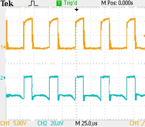
Figure 24. Diode D6 voltage waveform.
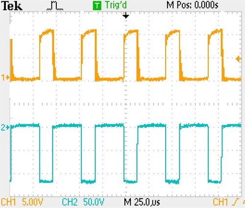
Figure 25. Diode D7 voltage waveform.
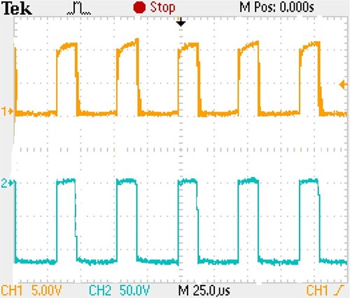
Figure 26. Source current waveform.
7. Conclusion
The non-isolated DC-DC high-gain converter suitable for renewable energy applications is proposed in this work. The power switches in the converter turned ON simultaneously make the inductor in the switched inductor cell charge the inductor with the source voltage. During turn OFF condition, the energy stored in the inductor is delivered to the load. The voltage multiplier cell in the converter is used to increase the output voltage and improves the voltage gain. The operating modes, steady-state analysis, voltage and current stress analysis and efficiency analysis are made. The converter's performance under closed-loop conditions is analyzed for varying source voltage, reference voltage and load power variations. The simulated and experimental efficiency of 96.54% and 95.2%, respectively, is achieved with a duty ratio of 27.3% under rated conditions. The continuous source current at the input side makes the converter suitable for renewable energy applications such as electric vehicles, UPS, light emitting diode and DC distribution systems.
Disclosure statement
No potential conflict of interest was reported by the author(s).
References
- Salvador MA, Lazzarin TB, Coelho RF. High step-up DC-DC converter with active switched-inductor and passive switched-capacitor networks. IEEE Trans Ind Electron. July 2018;65(7):5644–5654.
- Wu B, Li S, Liu Y, et al. A new hybrid boosting converter for renewable energy applications. IEEE Trans Power Electron. February 2016;31(2):1203–1215.
- Sadaf S, Al-Emadi N, Maroti PK, et al. A new high gain active switched network-based boost converter for DC microgrid application. IEEE Access. May 2021;9:68253–68265.
- Karthikeyan V, Kumaravel S, Gurukumar G. High step-up gain DC-DC converter with switched capacitor and regenerative boost configuration for solar PV applications. IEEE Trans Circuits Syst II. December 2019;66(12):2022–2026.
- Varesi K, Hassanpour N, Saeidabadi S. Novel high step-up DC-DC converter with increased voltage gain per device and continuous input current suitable for DC microgrid applications. Int J Circuit Theory Appl. April 2020;48(10):1–17.
- Athikka S, Sehgal K, Mohan U, et al. A voltage multiplier based non-isolated high gain DC-DC converter for DC bus application. International Conference on Futuristic Technologies in Control Systems & Renewable Energy (ICFCR), December 2020.
- Pourfarzad H, Saremi M, Jalilzadeh T. An extended high–voltage–gain DC-DC converter with reduced voltage stress on switches/diodes. Electrical Engineering, Springer, June 2020.
- Zhou M, Fu J, Wu X, et al. A non-isolated high-gain DC/DC converter suitable for fuel cell vehicles. J Electr Eng Technol. May 2021;17(1):271–282.
- Maalandish M, Hosseini SH, Ghasemzadeh S, et al. Six-phase interleaved boost dc/dc converter with high-voltage gain and reduced voltage stress. IET Power Electron. November 2017;10(14):1–11.
- Abdel-Rahim O, Wang H. A new high-gain DC-DC converter with model predictive-control based MPPT technique for photovoltaic systems. CPSS Trans Power Electron Appl. June 2020;5(2):191–200.
- Alzahrani A, Ferdowsi M, Shamsi P. A family of scalable non-isolated interleaved DC-DC Boost converters with voltage multiplier cells. IEEE Access. January 2019;7:11707–11721.
- Wang Y, Qiu Y, Bian Q, et al. A single switch quadratic boost high step-up DC-DC converter. IEEE Trans Ind Electron. June 2019;66(6):4387–4397.
- Pires VF, Cordeiro A, Foito D, et al. High step-up DC-DC converter for fuel cell vehicles based on merged quadratic Boost–Cuk. IEEE Trans Veh Technol. August 2019;68(8):7521–7530.
- Chandrasekar B, Nallaperumal C, Padmanaban S, et al. Non-Isolated high-gain triple port DC-DC Buck-Boost converter with positive output voltage for photovoltaic applications. IEEE Access. June 2020;8:113649–113666.
- Hammoda A, Buamud M, Tamasas ME, et al. Experimental verification and simulation of two stages positive output cascade boost converter super-lift DC/DC Luo- converter. 4th IEEE International Conference on Engineering Technologies and Applied Sciences (ICES), February 2018.
- Nguyen M-K, Duong T-D, Lim Y-C. Switched-capacitor-based dual-switch high-boost DC-DC converter. IEEE transactions on power electronics, May 2018, Vol. 33, Issue: 5, pp: 4181–4189.
- Tofoli FL, de Castro Pereira D, de Paula WJ, et al. Survey on non-isolated high-voltage step-up dc-dc topologies based on the boost converter. IET Power Electron. October 2015;8(10):2044–2057.
- Zhang N, Zhang G, See KW, et al. A single-switch quadratic Buck-Boost converter with continuous input port current and continuous output port current. IEEE Trans Power Electron. May 2018;33(5):4157–4166.
- Yang L-S, Liang T-J, Chen J-F. Transformerless DC-DC converters with High Step-up Voltage Gain. IEEE Trans Ind Electron. August 2015;56(8):3144–3152.
- Ahmad J, Siddique MD, Sarwar A, et al.. A high gain non-inverting DC-DC converter with low voltage stress for industrial applications. 2021;48(12):4212–4230.
- Samiullah M, Bhaskar MS, Meraj M, et al. High gain switched-inductor-double-leg converter with wide duty range for DC microgrid. IEEE Trans Ind Electron. October 2021;68(10):9561–9573.
- Tewari N, Sreedevi VT. A novel single switch DC-DC converter with high voltage gain capability for solar PV based power generation systems. Sol Energy. September 2018;171:466–477.
- Sri Revathi B, Samuel VJ, Mahalingam P. High step-up DC-DC converter based on double self-lift switched-coupled-inductor. Int J Electron. April 2022.