
 ?Mathematical formulae have been encoded as MathML and are displayed in this HTML version using MathJax in order to improve their display. Uncheck the box to turn MathJax off. This feature requires Javascript. Click on a formula to zoom.
ABSTRACT
Electrocatalyst-coated metallic electrodes for electrochemical flow reactors have many applications in electrosynthesis, environmental remediation and energy conversion. This work presents novel nickel-coated titanium-alloy electrodes produced by means of direct metal laser sintering and constant current electrodeposition in an additive-free Wood’s nickel strike then a Watts nickel bath. Several 3D porous architectures were created in Ti-6Al-4 V alloy and coated, their digital design being the subject of previous work. Nickel coatings were macroscopically uniform and adherent with a thickness up to 5.8 µm, depending on the surface area of the electrodes. The morphology of nickel was cauliflower-like, with crystallisation growth occurring as spherical grains, as typically found for deposits from pH buffered Watts baths. Some degree of coating porosity was observed at electrodes of large surface area, indicating the need for longer deposition times. The results open the path for further optimisation of electrodeposition parameters and the development of bath additives to tailor deposit properties.
Introduction
Porous metal electrodes have found diverse applications in electrochemical processing, including industrial electroplating, water electrolysis, treatment of wastewaters, energy storage and large-scale production of commodity chemicals.Citation1,Citation2 Such electrodes offer extended surface area, enhanced mass transfer, robust mechanical properties and a great diversity of materials and functional coatings, making them well-suited for use in electrochemical flow reactors.Citation3 New electrodes, based on metallic substrates, have been increasingly applied in the topical fields of power-to-chemicals, Citation4 water electrolysis,Citation5 flow batteries,Citation6 and carbon dioxide capture.Citation7
3D-printing opens an innovative path to the development of periodic, open-cell porous electrodes to complement or surpass classic metal manufacture techniques.Citation1,Citation8,Citation9 Laser sintering methods are particularly suitable to produce such substrates, as they allow a high degree of surface control and design flexibility.Citation10 These benefits enable the possibility of multi-scale development and aid the validation of mathematical models for structured materials.Citation11 Indeed, 3D-printing permits digital customisation of the shape and size of the open-cells that form the scaffold of the porous electrode, effectively tailoring its electrochemical performance. An iterative, ‘virtuous cycle’ of electrode design incorporating new catalytic coatings is also feasible.Citation12
Several 3D-printed metal electrodes with functional coatings have been recently reported.Citation13 As a coating technique, electrodeposition continues to provide the advantages of relative simplicity and low cost, with many proven and commercial methodologies. Examples of such coatings on 3D-printed electrodes include nickel on stainless steel,Citation12,Citation14,Citation15 platinum on stainless steel,Citation16 nickel on titanium,Citation17 and platinum on titanium.Citation18 These metals provide an electrocatalytic surface for designated electrode reactions in electrochemical flow reactors.Citation19
Nickel-coated titanium (Ti/Ni) has a number of niche applications due to its favourable mechanical properties, low density and good corrosion resistance; an example is orthodontic wires.Citation20 Although less common than for nickel-coated stainless or mild steel production,Citation21,Citation22 the buffered Watts nickel bath has been considered as a robust, well-established route to deposit nickel on titaniumCitation23 and modified versions of it can be used to produce Raney nickel on titanium.Citation24 Bright nickel has been produced on titanium from baths containing chloride and ammonium ions with thiourea as an additive.Citation25 Nickel has also been deposited on the common Ti-6Al-4 V alloy using a modified Watts bath and subjected to a heat treatment for improved wear resistance.Citation26 Following the above trend, a citrate-based bath has been used to deposit nickel on a 3D-printed, Grade 2 titanium texturised surface.Citation17
This work reports the galvanostatic electrodeposition of nickel on 3D-printed, open-cell titanium alloy structures intended for flow-through and flow-across porous electrodes in innovative electrochemical reactors. To the best of the authors’ knowledge, this concept is presented for the first time and builds on previously reported non-cellular arrays of 3D-printed Ti/Ni pillars for water splitting.Citation17 Nickel coatings are applied first from a ‘Wood’s strike’ then from an additive-free ‘Watts bath’, see a). This approach avoids the formation of an oxide layer on the titanium alloy and provides an electrocatalytic surface to support targeted reactions, such as a cathode for water electrolysis, oxidation of pollutants or any other suitable electrode reaction. The porous electrode architectures were developed and optimised in a previous work,Citation27 which considered the determination of surface area and volumetric properties through X-ray computed tomography as well as the measurement of permeability to flowing electrolytes. Future work will demonstrate the performance of optimised, catalytic electrodes in an electrochemical flow cell.
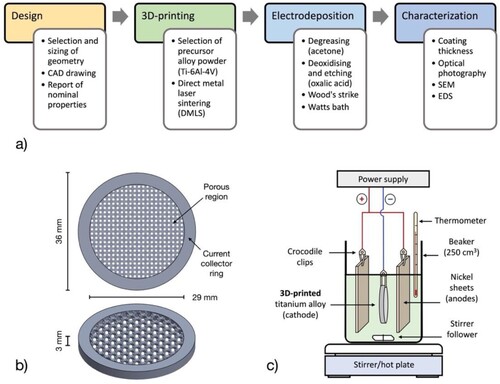
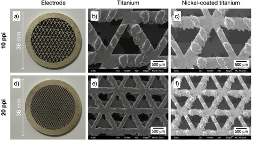
Figure 1. 3D-printed, Ti/Ni porous electrodes for electrochemical flow reactors. a) Design and coating process. b) Configuration of the 3D-printed titanium substrates, front view and perspective (10 ppi rectangular porous architecture as example). c) Experimental arrangement for the electrodeposition of electrocatalytic nickel on titanium substrates.
Materials and methods
Design and manufacture of electrode structures
The porous architectures were developed following a proposed ‘virtuous cycle’ for electrode materials manufacture,Citation28 having rectangular, hexagonal or triangular periodic open-cells. These were organised in a body-centred spatial configuration, with cell sizes between 0.7 mm to 2.6 mm and equivalent to porosity grades of 10, 20 and 30 pores per linear inch (ppi), as is normally reported for off-the-shelf metal and ceramic foams as well as for reticulated vitreous carbon (RVC).Citation29 Full drawings and dimensions for each porous structure can be found elsewhere.Citation27 The geometries were designed using the Solid Works CAD suite (Dassault Systèmes, France), their nominal dimensions and main properties are given in . As shown in b), the 3D-printed electrodes had a thickness of 3 mm and a diameter of 36 mm, the ‘porous region’ being 29 mm in diameter (projected surface area = 6.61 cm2, volume = 1.98 cm3) and surrounded by a solid ‘ring’ used as both structural support and current collector. The nominal, total surface area of each 3D-printed electrode is the sum of the surface area of its porous region and the surface area of the ring. The surface area of each ‘porous region’ is the product of its volumetric surface area (reported previouslyCitation27) and the fixed volume of the ‘porous region’. The surface area of the ‘ring’ (13.27 cm2) is calculated by considering it a rectangular hollow cylinder (external diameter = 36 mm, internal diameter = 29 mm). The CAD designs were sent to a 3D-printing service (Proto Labs, UK) and produced through direct metal laser sintering (DMLS) from a Ti-6Al-4 V alloy powder (maximum of 6.7% aluminium, 4.5% vanadium and 0.3% iron in mass). The layer-by-layer process provided a resolution of 20 µm and a void fraction within the solid material under 5 × 10⁻⁴.
Table 1. Nominal characteristics of the open-cell architectures and relevant surface areas of the coated electrodes according to CAD. Volumetric porosity and volumetric surface area are taken from previous work.Citation27
Solutions and substances
All substances used in pretreatment processes and electrodeposition baths were reagent or analytical grade and used as received. Salts and acids were sourced from Thermo Fisher Scientific, USA, with the exception of oxalic acid, which was sourced from Acros Organics, USA. All the solutions were prepared using deionised water with a conductivity of 18.2 MΩ cm.
Surface pretreatment
The titanium substrates were subjected to a surface pretreatment consisting of immersion for 5 min at 22 °C in acetone, 5 min in 10 mol dm−3 sodium hydroxide and 2 min in 6 mol dm−3 hydrochloric acid.Citation18 This was followed by an etching step to remove surface oxide using a 10% w/v oxalic acid solution at 80 °C for 45 min. During this step, the solution was kept under constant stirring at 150 rev min−1 using a 25 mm long, 5 mm diameter cylindrical, PTFE-coated steel stirring bar and a stirrer hot plate. The etched pieces were thoroughly rinsed with deionised water.
Electrodeposition of nickel
The catalytic nickel coating was applied to the titanium substrates in two galvanostatic steps performed at a temperature of 50 °C immediately after surface pretreatment. Nickel nucleation was first induced in an acidic ‘Wood’s strike’ bath at a current of 2 A for 2 min before proceeding to a more controlled electrodeposition in a buffered ‘Watts bath’ at a current of 1 A for 8 min. The Wood’s bath had a composition of 240 g dm−3 NiCl2•6H2O and 100 cm3 dm−3 concentrated HCl (pH ≈ 0.1), while the Watts bath was a solution of 260 g dm−3 NiSO4•7H2O, 50 g dm−3 NiCl2•6H2O and 30 g dm−3 H3BO3 (pH ≈4.5).Citation21 The reduction of nickel ions takes place along with hydrogen evolution, according to the following electrode reactions:Citation30
(1)
(1)
(2)
(2) It has been reported that nickel reduction on titanium in a Watts bath displays a current efficiency, ϕ, of approximately 98% at current densities under 100 mA cm−2.Citation24 A ϕ value of 95% was assumed for the Wood’s strike. Using these procedures, the titanium substrates were immersed in the centre of a 250 cm3 beaker under constant stirring at 150 rev min−1 and connected as cathodes (negative electrode), see c). Two pieces of 99.5% nickel foil of 5 cm × 10 cm and a thickness of 250 µm (Alfa Aesar, UK) were used as soluble anodes (positive electrodes), each of them facing one side of the 3D-printed electrode with a separation of 2 cm. Nickel-coated steel crocodile clips were used to connect the working electrodes by their edge to a QL355T direct current power supply (ThurlbyThandar, UK). The resulting Ti/Ni electrodes were rinsed with deionised water and dried.
The nominal thickness of the coatings, x, was calculated by applying Faraday’s laws of electrolysis and the knowledge of the density, ρ, of nickel (8.907 g cm−3):Citation31
Where M is the molar mass of nickel (58.69 g mol−1), I is current, t is time, A is surface area, z is electron stoichiometry, and F is Faraday’s constant (96485.3 C mol−1).
SEM imaging
SEM images of the morphologies at the surfaces of interest were obtained with JSM-6500F (JEOL, USA) and EVO50 (Carl Zeiss, Germany) instruments. EDS analysis was performed using a Quantax (Brucker Nano, Germany) detector fitted to the EVO50 microscope.
Results and discussion
Controlled porosity and architecture of titanium substrates
The general appearance of an uncoated titanium alloy substrate and a nickel-coated electrode before and after electrodeposition is shown in . The coated Ti/Ni 3D-printed electrodes are presented grouped by the shape of their open-cell architecture as follows: for the rectangular type, for the hexagonal type, and for the triangular type. Macroscopically, all electrodes have a uniform granular texture and are free of significant distortion. SEM images of the 3D-printed titanium alloy substrates taken after their manufacture and before their pre-treatment are labelled as ‘titanium’ in . These surfaces are relatively smooth, free of laser beam melt lines or clear micropores, consistent with the resolution of 20 µm. In contrast, rough substrates were produced at the same scale in stainless steel 316 specimens of the same electrode architectures.Citation27 In that case, the melt lines were evident and the surfaces were speckled with nodules of molten material under 10 µm in diameter. The surface of 3D-printed titanium substrate is more homogeneous and less rough, likely as a result of dissimilar DMLS parameters in combination with the melting properties of the two alloys in question.
Figure 2. Photographs of the 3D-printed porous electrodes with triangular 20 ppi architecture before and after the coating procedure. a) 3D-printed titanium alloy substrate. b) After nickel electrodeposition.
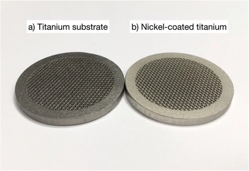
Figure 3. Photographs and SEM images of 3D-printed porous electrodes with rectangular open-cell architecture. SEM magnification 30×. a) Ti/Ni electrode with porosity grade 10 ppi: b) bare titanium alloy, c) nickel-coated. d) Ti/Ni electrode with porosity grade 20 ppi: e) bare titanium alloy, f) nickel-coated. g) Ti/Ni electrode with porosity grade 30 ppi: h) bare titanium alloy, i) nickel-coated.
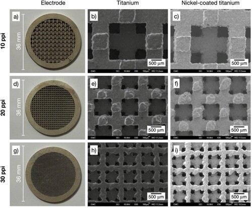
Figure 4. Photographs and SEM images of 3D-printed porous electrodes with hexagonal open-cell architecture. SEM magnification 30×. a) Ti/Ni electrode with porosity grade 10 ppi: b) bare titanium alloy, c) nickel-coated. d) Ti/Ni electrode with porosity grade 20 ppi: e) bare titanium alloy, f) nickel-coated.
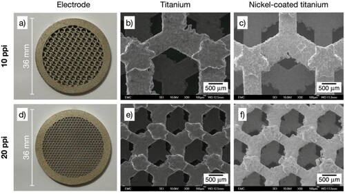
Figure 5. Photographs and SEM images of 3D-printed porous electrodes with triangular open-cell architecture. SEM magnification 30×. a) Ti/Ni electrode with porosity grade 10 ppi: b) bare titanium alloy, c) nickel-coated. d) Ti/Ni electrode with porosity grade 20 ppi: e) bare titanium alloy, f) nickel-coated.
At a sub-millimetre scale, individual open-cells and their struts display the irregularities that are commonly produced by DMLS methods, deviating from straight edges with protrusions of up to approximately 200 µm. Moreover, some overall shape distortion is evident in the 20 ppi hexagonal architecture, see e). However, the electrodes are considered uniform at the relevant scales and suitable for the intended electrochemical applications, noting that common metal foams display random shapes and a much broader distribution of open-cell dimensions.Citation29 Additional manufacture accuracy for 3D-printed metals can be achieved by implementing a finer control of DMLS parameters.
Nickel coatings on titanium substrates
As shown in , the dark grey of a titanium surface was replaced by the slightly gold-tinged silver colour that is characteristic of nickel. Images of the Ti/Ni 3D-printed electrodes are shown in a), 3d), and 3g) for the rectangular architectures, a) and 4d) for the hexagonal architectures, and a) and 5d) for the triangular architectures. SEM images of the Ti/Ni 3D-printed electrodes at a magnification of 30× before and after electrodeposition are labelled as ‘titanium’ and ‘nickel-coated titanium’ in . The presence of the coating is qualitatively confirmed by the increase in the brightness of the SEM image of the Ti/Ni 3D-printed electrodes compared to the bare titanium alloy, which is related to the conductivity of the metal under analysis. See below for EDS analysis.
A slight increase in roughness can be seen at a magnification of 30× in all the ‘nickel-coated titanium’ images as a result of the etching and subsequent growth of nickel on the titanium alloy substrates. However, it is evident that the substrates retain their integrity after the pretreatment in oxalic acid solution under the chosen conditions. The appearance of cracks and unnecessary titanium dissolution is more difficult to control when boiling HCl solutions are used during pretreatment.Citation32 Wood’s strike, originally developed to activate stainless steels, was here intended to induce nucleation of fine grains in a chloride-rich environment,Citation21 although it might have only a small effect on titanium in these conditions since similar deposits to the ones observed here have been produced using Watts bath only.Citation23 Overall, the etching, followed by the Wood’s strike and the electrodeposition in the Watts bath produced thin, adherent nickel deposits.
By considering the total surface area of each 3D-printed electrode, see , the thickness of the nickel coating can be estimated from the knowledge of the applied current and current efficiency. The values are reported in . The nickel thickness at the 3D-printed electrodes ranges from 2.4 µm to 5.8 µm, with the electrodes with larger surface areas having thinner coatings. This is sufficient for non-demanding applications in the laboratory. For perspective, a typical nickel layer for hydrogen evolution research has a thickness of 15 µm.Citation33 However, thicker coatings are certainly needed for improved durability, such as those for corrosion protection, usually at 120 µm for nickel.Citation34
Table 2. Nominal coating thicknesses calculated from the electrodeposition parameters and the nominal surface area of the 3D-printed electrodes under the assumption of a uniform current distribution.
Morphology and composition of nickel coatings
The microstructure of the nickel coatings in different zones of one of the electrodes (20 ppi triangular) is further analysed in . A cauliflower morphology is observed at the relatively planar surface of the current collector ring. The overlapping spherical nickel grains have sizes between 2 and 5 µm, as seen at a magnification of 2000×, c). Very similar deposits have been reported on 3D-printed commercially pure titanium from a nickel sulphate solution containing a citrate additive,Citation17 suggesting a modest effect of citrate under the reported conditions. These morphologies are expected for additive-free Watts baths and contrast with the smooth bright-nickel achieved with commercial baths, e.g. nickel coating on stainless steel.Citation35 The high current efficiency of nickel deposition is supported by the absence of a spongy morphology, which is often found when hydrogen evolution dominates at high current densities.Citation36,Citation37
Figure 6. SEM images of the nickel coating on the 3D-printed porous electrode with triangular 20 ppi architecture at different locations and magnifications. At a mid-point in the current collector: a) 100×, b) 1000×, c) 2000×. At a point near the centre of the porous structure of the electrode: d) 100×, e) 1000×, f) 2000×.
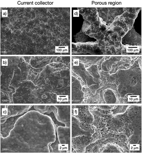
In contrast, coating porosity can be observed on the 20 ppi triangular 3D-printed electrode in the area denominated ‘porous region’, see b). As shown in e) and f), in this area the cauliflower morphology is replaced by an aggregation of spherical nickel grains between 1 and 2 µm in diameter, which are the result of radial growth of nickel nuclei in acidic solutions.Citation38 The coating porosity is likely caused by the low local current density in this part of the electrode, which has also the highest surface area. A strict validation of the coating thickness is outside the scope of this work but it is notable that the apparent thickness of the incomplete coating in f) is consistent with the nominal value of 2.4 µm calculated for this 3D-printed electrode, see .
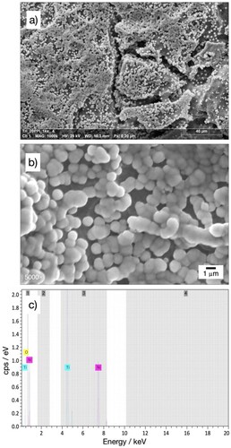
The ‘porous region’ of the 20 ppi triangular 3D-printed electrode is shown in a) and b) together with its corresponding EDS spectrum in c). The coating morphology is similar as above. The spherical grains are characteristic of nickel nucleation on titanium from sulphate-chloride solutions,Citation38 and suggest the predominant preferred orientation is Ni(111).Citation23 This can be contrasted to the faceting and platelet-like morphologies and crystal preferred orientation Ni(100) observed for nickel electrodeposition on copper from a methane sulphonic acid solution.Citation39 Spine growth might eventually form at longer electrodeposition times, as in the case of a nickel substrate coated from a Watts bath.Citation40 The elemental composition of the nickel coating and the underlying titanium substrate is confirmed by the EDS in c). The spectrum confirms a partial exposure of the underlying titanium and is comparable to that of the porous nickel coating on 3D-printed Grade 2 titanium.Citation17 In these cases, a full coating could easily be achieved by extending the duration of electrodeposition. Further modification of the grain shape and size is possible by using appropriate bath additives.Citation41
Figure 7. High magnification SEM images and EDS of the nickel coating on the 3D-printed porous electrode with triangular 20 ppi architecture at a mid-point in the porous region. a)1000× image, and c) corresponding EDS spectra. b) Coating microstructure at 5000× magnification.
Conclusions
Nickel coatings have been successfully electrodeposited on 3D-printed type Ti-6Al-4 V titanium alloy using Wood’s strike followed by an additive-free Watts nickel bath. The production of electrocatalytic nickel coatings on porous cellular titanium substrates for electrochemical reactors by direct metal laser sintering (DMLS) has been demonstrated. The resulting Ti/Ni electrodes can be applied in a flow-across cell configuration as optimised architectures for efficient bipolar flooded or trickle tower electrochemical reactors for electrosynthesis and pollution control.Citation42 This work also confirms the possibility of applying functional nickel coatings on 3D-printed titanium alloy components for a wide range of metal finishing applications.Citation22 The coatings are macroscopically uniform, with a cauliflower-like microstructure. However, some degree of coating porosity was observed in non-planar regions of the electrodes, indicating opportunities for further optimisation of the electrodeposition parameters. The use of more suitable electrodeposition baths should be considered, using levelling and brightening additives to control electrocrystallisation and the morphology of nickel.
Acknowledgements
This work was supported by King Saud University, Riyadh (Saudi Arabia) under Researchers Supporting Project number RSPD2023R612. BMA thanks CONACYT (Mexico) for scholarship number 468574 and for sponsoring a visit to the University of Southampton (UK). LFA thanks Prof. Thomas Turek and Mr. Sascha Genthe for providing access to the SEM facilities at Clausthal University of Technology (Germany).
Disclosure statement
No potential conflict of interest was reported by the author(s).
References
- C.-Y. Lee, A. C. Taylor, A. Nattestad, S. Beirne and G. G. Wallace: Joule, 2019, 3, 1835–1849.
- V. Egorov and C. O’Dwyer: Curr. Opin. Electrochem., 2020, 21, 201–208.
- L. M. Abrantes: Three-dimensional electrode, in ‘Encyclopedia of applied electrochemistry’, Springer, 2014, pp. 2077–2081.
- B. H. R. Suryanto, H.-L. Du, D. Wang, J. Chen, A. N. Simonov and D. R. MacFarlane: Nature Catalysis, 2019, 1–7.
- V. Hoffmann, L. Hoffmann, W. Schade, T. Turek and T. Gimpel: Int. J. Hydrogen Energy, 2022, 47, 20729–20740.
- R. D. Wolf, M. D. Rop and J. Hereijgers: ChemElectroChem, 2022, 9, e202200640.
- M. Park and W. Shin: J. CO2 Utilization, 2021, 45, 101435.
- X. Tian and K. Zhou: Nanoscale., 2020, 12, 7416–7432.
- P. Nyamekye, P. Nieminen, M. R. Bilesan, E. Repo, H. Piili and A. Salminen: Appl. Mater. Today, 2021, 23, 101040.
- D. D. Gu, W. Meiners, K. Wissenbach and R. Poprawe: Int. Mater. Rev., 2012, 57, 133–164.
- S. M. Hashemi, S. Parvizi, H. Baghbanijavid, A. T. L. Tan, M. Nematollahi, A. Ramazani, N. X. Fang and M. Elahinia: Int. Mater. Rev., 2022, 67, 1–46.
- F. C. Walsh, L. F. Arenas and C. Ponce de León: Trans. IMF., 2020, 98, 65–72.
- M. P. Browne, E. Redondo and M. Pumera: Chem. Rev., 2020, 120, 2783–2810.
- L. F. Arenas, C. Ponce de León and F. C. Walsh: Electrochem. Commun., 2017, 77, 133–137.
- A. Ambrosi and M. P. Pumera: ACS Sustainable Chem. Eng., 2018, 6, 16968–16975.
- A. Ambrosi and M. Pumera: Adv. Funct. Mater., 2018, 28, 1700655.
- C.-Y. Lee, A. C. Taylor, S. Beirne and G. G. Wallace: Adv. Mater. Technol., 2019, 4, 1900433.
- L. F. Arenas, N. Kaishubayeva, C. Ponce de León and F. C. Walsh: Trans. IMF., 2020, 98, 48–52.
- A. Ambrosi, R. R. S. Shi and R. D. Webster: J. Mater. Chem. A, 2020, 8, 21902–21929.
- H. Kim and J. W. Johnson: Angle Orthod., 1999, 69, 39–44.
- G. A. Di Bari: Electrodeposition of nickel in ‘Modern electroplating’, 5th edn, Wiley, 2010, pp. 79–114.
- S. Wang, N. Zhou and F. C. Walsh: Trans. IMF, 2016, 94, 274–282.
- C.-C. Hu, C.-Y. Lin and T.-C. Wen: Mater. Chem. Phys., 1996, 44, 233–238.
- M. Cooper and G. G. Botte: J. Mater. Sci., 2006, 41, 5608–5612.
- L. Yuan, J. Hu, Z. Ding and S. Liu: Int. J. Electrochem. Sci., 2017, 12, 7312–7325.
- M. Abdoos, A. A. Amadeh and M. Adabi: Trans. IMF., 2019, 97, 146–154.
- N. Kaishubayeva, C. Ponce de León, F. C. Walsh and L. F. Arenas: J. Chem. Technol. Biotechnol., 2021, 96, 1818–1831.
- F. C. Walsh, L. F. Arenas and C. Ponce de León: Curr. Opin. Electrochem., 2019, 16, 10–18.
- L. F. Arenas, R. P. Boardman, C. Ponce de León and F. C. Walsh: Carbon, 2018, 135, 85–94.
- J. Vazquez-Arenas, L. Altamirano-Garcia, M. Pritzker, R. Luna-Sánchez and R. Cabrera-Sierra: J. Electrochem. Soc., 2011, 158, D33–D41.
- D. Barker and F. C. Walsh: Trans. IMF., 1991, 69, 158–162.
- K. Kugler, M. Luhn, J. A. Schramm, K. Rahimi and M. Wessling: Phys. Chem. Chem. Phys., 2015, 17, 3768–3782.
- D. M. Soares, O. Teschke and I. Torriani: J. Electrochem. Soc., 1992, 139, 98–105.
- S. R. Taylor: Coatings for corrosion protection: Metallic, in ‘Encyclopedia of Materials: Science and Technology’, Pergamon, 2001, pp. 1269–1274.
- M. I. Jaramillo-Gutiérrez, S. M. Sierra-González, C. A. Ramírez-González, J. E. Pedraza-Rosas and J. A. Pedraza-Avella: Int. J. Hydrogen Energy, 2021, 46, 7667–7675.
- K. I. Siwek, S. Eugénio, D. M. F. Santos, M. T. Silva and M. F. Montemor: Int. J. Hydrogen Energy, 2019, 44, 1701–1709.
- N. D. Nikolić, V. M. Maksimović and L. Avramović: Metal, 2021, 11, 859.
- F. Lantelme, A. Seghiouer and A. Derja: J. Appl. Electrochem., 1998, 28, 907–913.
- N. M. Martyak and R. Seefeldt: Plat. Surf. Finish., 2004, 32–37.
- J. Záchenská, M. Ábel, M. Mičušík, V. Jorík and M. Zemanová: J. Appl. Electrochem., 2020, 50, 959–971.
- U. S. Mohanty, B. C. Tripathy, P. Singh, A. Keshavarz and S. Iglauer: J. Appl. Electrochem., 2019, 49, 847–870.
- F. C. Walsh, L. F. Arenas and C. Ponce de León: J. Electrochem. Soc., 2021, 168, 023503.