
ABSTRACT
To understand adhesive bonds and their macroscopic behavior, a new experimental method is presented in this paper that allows to investigate micromechanical effects down to nanometer scale under load. The method combines ion milled cross sections, low-voltage scanning electron microscopy (SEM), digital image correlation, and a miniaturized testing machine in the SEM-chamber. Experimental results from shear-loaded adhesively bonded carbon fiber-reinforced polymer specimens illustrate the method’s benefits. Through a plasma etching process, the specimen cross section is textured, creating a stochastically distributed speckle pattern visible in SEM images. A miniaturized testing machine placed in the SEM is used to apply a load to the specimens while capturing images simultaneously. The resulting image series can be analyzed by image correlation algorithms. This method enables precise statements regarding strain distribution on the specimen at micro- and nanometer scales. While conventional coupon tests on bonded specimens can only depict the effects of a composite in a homogenized manner, the new method allows to gain additional insights into the underlying mechanisms.
1. Introduction
Due to their outstanding lightweight construction properties, carbon fiber-reinforced polymers (CFRP) have become a key component in modern aircraft construction.[Citation1] Adhesive bonding is a joining technology that offers considerable advantages for these types of materials. However, its reproducible and thereby reliable application for structural components in aerospace is still subject of nowadays research. In this context, a fundamental remaining issue is the lack of reliable predictions about crack growth and damage behavior in the bondline.[Citation2,Citation3]
Commonly, material tests on coupon level which are defined by several ASTM International and ISO standards are used for process qualification in aerospace industry.[Citation2] Due to the geometry of these specimens, typically spanning several centimeters, effects at the micrometer-scale can only be gathered in a superimposed manner. This is particularly problematic for a material like CFRP, which is characterized by pronounced microscale heterogeneity. This challenge is further exacerbated when considering structural bonding as a joining technology, introducing yet another additional component at the micrometer scale, namely the adhesive layer.
Digital image correlation (DIC) is a widely employed tool for analyzing materials as well as components and is a promising method to obtain crack paths. DIC provides full-field strain acquisition without direct contact with the specimen.[Citation4] Its use has therefore become extensively established in materials testing, primarily utilizing digital cameras equipped with charge-coupled device sensors. These cameras allow the use of different lenses for various magnifications from several meters to a few millimeters.[Citation5–7] However, at very high magnifications, which are necessary for investigations in the micrometer-scale, these devices encounter limitations. Optical cameras fail to deliver the resolution required for detailed measurement of strain distribution in thin adhesive layers. For this purpose, the utilization of scanning electron microscopy (SEM) to produce images for DIC investigations is of interest. Several publications have demonstrated the successful implementation of DIC on SEM images, as detailed in Chapter 3.1. However, the method of image generation presents challenges, particularly in terms of distortions and noise.[Citation8] What most studies have in common is that, predominantly, only metals and other conductive materials have been investigated, with relatively little attention given to polymers. However, there are particular challenges here as these materials tend to charge in the SEM, and SEMs with high acceleration voltages are not suitable for their investigation. The generation of a stochastic pattern for image recognition is also subject to limitations with polymer materials.
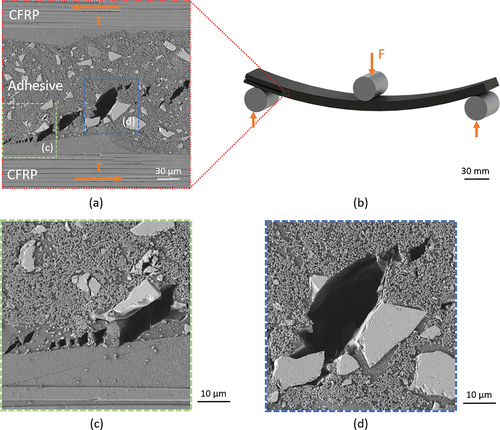
This paper introduces a digital image correlation method for measuring strains in shear-loaded adhesively bonded composites at the micro- and nanometer-scale. In this approach, miniaturized end-notched flexure specimens (ENF) are subjected to in-situ testing within a test chamber of a low-voltage field emission scanning electron microscope. This setup allows for the real-time high-resolution observation of the adhesive bond under load and the formation of micro-damage in detail, e.g. the formation of microcracks in a shear-loaded adhesive layer, as it is shown in . The distinctive hackle pattern observed is characteristic for shear-loaded adhesive layers and has been previously documented on fracture surfaces, as described by Chai.[Citation9] The method can also be used to investigate material inhomogeneities, e.g. the influence of fillers, and the morphology of the joining parts on the damage behavior of the bond. Furthermore, a series of images at different load levels generated in the SEM can be analyzed with image correlation algorithms to quantitatively measure the strain distribution at the micrometer or even nanometer scale.
Figure 1. (a) Formation of microcracks in a shear-loaded adhesively bonded CFRP joint (SEM cross section image). (b) Schematic representation of a conventional ENF sample. Cross section images (c) and (d) show enlarged sections of image (a) respectively.
This paper outlines the manufacturing of the miniaturized specimens, the generation of a speckle pattern for DIC, and the experimental procedure of material testing in a SEM.
2. Materials and manufacturing process
2.1. Materials
The adherends were made of Hexcel 8552/IM7 prepreg (Hexcel Corporation, Stamford/CT, USA), which is an epoxy-based thermoset CFRP that is widely used in aerospace applications. The quasi-isotropic layer build-up with [0/+45/90/-45]s results in 1 mm thick laminates. Curing was carried out according to the manufacturer’s specifications using a vacuum bag and an autoclave at 180°C and 0.5 MPa.[Citation10]
By using different manufacturing aids such as release films and peel ply on top of the prepreg lay-up, different surface morphologies were created. The used products were release film A5000 (Diatex, Lyon, France), peel ply ReleaseEase (Airtech, Huntington Beach/CA, USA), and peel ply 08940 (UTT Indorama Ventures Mobility Group, Krumbach, Germany).
Specimens were bonded using Henkel LOCTITE EA 9396 AERO (Henkel AG & Co. KGaA, Düsseldorf, Germany), an epoxy paste adhesive without fillers.[Citation11]
2.2. Specimen manufacturing
Initially, the CFRP joining parts underwent a surface pretreatment to ensure good adhesion.[Citation12] Therefore, the samples were first cleaned and degreased with isopropanol (>95%, SAV Liquid Production, Flintsbach, Germany) and then pretreated with low-pressure plasma. This physical surface pretreatment consistently results in high adhesive strengths on polymers.[Citation13,Citation14] The low-pressure plasma treatment was performed via the device type Diener Nano SL PC (Diener Electronic GmbH & Co. KG, Ebhausen, Germany) using oxygen as process gas with a treatment duration of 20 minutes. The applied output power was set to 300 W with a gas flow of 200 sccm.
Since the specimens have little dimensions, the shape tolerance must be particularly tight. This applies not only to the external dimensions of the specimens but also to the thickness of the adhesive layer, as well as the position and shape of the artificial crack according to the ENF specimen geometry. For the latter, preliminary tests have revealed that a release film, when placed between the joining parts and subjected to curing under applied pressure, tends to shift out of position. When a self-adhesive film is utilized as an insert, the adhesive of the film forms a soft zone beneath the film and around its tip within the structural adhesive layer. It can be assumed that this soft substance significantly influences the stress state in the investigated area in the structural adhesive layer and should therefore be avoided.
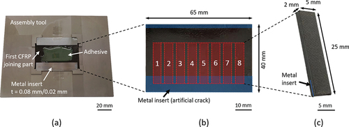
Therefore, a steel insert was used, which was previously coated with Frekote 55NC release agent (Henkel AG & Co. KGaA, Düsseldorf, Germany).[Citation15] This enables a shape-stable artificial crack and a very precisely adjustable adhesive layer thickness. A custom-made assembly tool guarantees the proper fixation of all components in their designated positions ().
Figure 2. Manufacturing of reduced-size end-notched flexure specimens: (a) Assembly of the adhesive joint. (b) Bonded plate after hot pressing and cutting of the red highlighted test specimens. (c) Miniaturized ENF specimen.
The further workflow of the specimen manufacturing is schematically outlined in and is explained in detail in the following.
Figure 3. Workflow for the manufacturing of reduced-size end-notched flexure specimens.
After positioning the lower joining part and the metal inserts in the assembly device, adhesive was applied and spread on the joining part using a spatula. Subsequently, the upper joining part was inserted into the assembly device and the entire assembly was placed in a hot press for curing (66°C for 60 min). Subsequent to the curing process, individual specimens were cut out from the initially bonded plate using a diamond wire saw (). The outer contour of the specimens was then ground to size with a cup grinder, ensuring very high shape accuracy. The specimens were cut in such a manner that the length of the insert was 5 mm (). After cutting, the sides of the specimens were mechanically polished on a grinding disk (1 µm diamond polishing suspension), and an oxygen plasma etching process was applied. This process generates a suitable speckle pattern on the polymer surface for digital image correlation, which will be discussed in more detail in Chapter 3.1.
3. Digital image correlation of loaded specimens inside a SEM
Testing of specimens is realized inside a SEM, as shown schematically in . For this purpose, a Zeiss Ultra Plus SEM (Carl Zeiss AG, Oberkochen, Germany) with a field emission gun was used. This low-voltage SEM allows imaging of polymers without the need of coating the samples with conductive materials beforehand. One advantage of a low acceleration voltage is in this regard that even very fine surface structures can be recorded.[Citation16] Images were captured at a 0.8 kV accelerating voltage using the in-chamber Everhart-Thornley secondary electron (SE) detector, with detector’s collector grid voltage set at 300 V.
Figure 4. Schematic of the specimen preparation and testing procedure: (a) Miniaturization of the test specimens. (b) In-situ testing in the scanning electron microscope. (c) Evaluation of the image series by means of DIC.
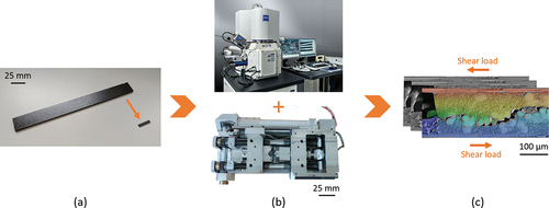
Material testing was conducted using a miniaturized tension-compression module manufactured by Kammrath & Weiss GmbH (Schwerte, Germany). Its compact design enables operation within the vacuum chamber of an SEM, while a custom-made adapter enables the execution of three-point bending tests.
For the evaluation of the SEM images by means of digital image correlation, the software GOM Correlate Pro (Carl Zeiss IQS Deutschland GmbH, Oberkochen, Germany) was employed.
3.1. Pattern generation for DIC
Digital image correlation relies on pattern recognition within the image series. This requires a stochastically distributed pattern with high contrast to be present on the image of the sample. For conventional DIC on a macroscopic scale, spray paint is typically used for this purpose, e.g. applied with an airbrush gun. Nevertheless, the use of spray paint is not feasible on a micrometer scale since a pattern cannot be finely applied with sufficient precision using this method. Moreover, in SEM images, contrast is influenced by factors such as the type of detector, acceleration voltage, sample surface inclination, electrical charges, and the atomic number of the material under investigation.[Citation17] Consequently, a high optical contrast visible to the eye does not necessarily lead to a high contrast level in the SEM image.
Various approaches for the generation of a pattern visible in the SEM can be found in the literature. If the sample exhibits an inhomogeneous structure this can be used as pattern, as it is demonstrated by Jin et al.[Citation18]
If the specimen lacks a high-contrast structure on the required scale, artificial application of particles is conceivable. For example, colloidal silica, zirconia, and yttria-stabilized zirconia in suspension can be used for this purpose, as e.g. described by Wachi et al.[Citation19] and Yin et al.[Citation20]
Physical vapor deposition (PVD) of metallic particles is shown by Hoefnagels et al.[Citation21] The authors use an indium-tin alloy, which spontaneously forms small islands upon deposition onto the surface. This particular alloy eliminates the need for heat treatment of the sample, which would otherwise be required with other metals to induce the transformation of an initially homogeneous layer into individual islands.
Jin et al.[Citation18] demonstrate the utilization of a lithographically fabricated metallic grid as a stencil for creating a pattern through PVD. Various materials can be used in this process, since no island growth needs to occur. However limitations arise from the mesh density of commercially available grids. In addition, the specimens must be flat and the grid must be tight against the specimen to ensure a neat imprint.
Another option is to create a structure within the material. For this purpose, focused ion beam (FIB)[Citation22] or electron beam lithography[Citation23] can be employed.
This, however, requires sophisticated technology and, in the case of FIB, involves extended processing times due to multiple repetitions of the machining process.
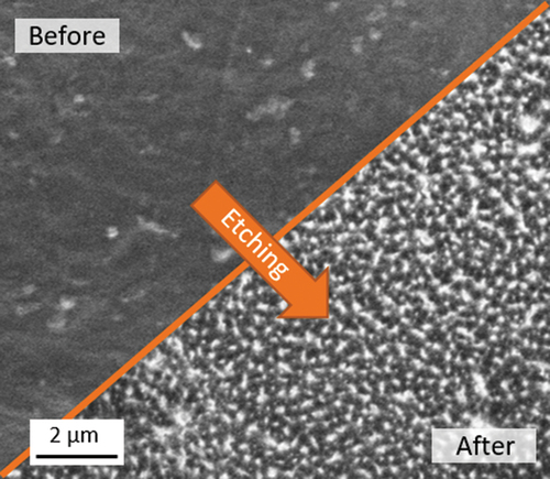
In this study, a method was used to create a non-repetitive and isotropic pattern on polymers without the need for applying any additional material. For this purpose, the specimen was treated with low-pressure oxygen plasma, inducing surface roughening on a nanometer scale. This results in randomly distributed peaks on the surface, as depicted in exemplarily. Due to the edge effect in a SE image, protrusions and edges emit more SE and therefore appear brighter in images.[Citation17] Consequently, the peaks on the surface appear brighter than the background. By appropriately adjusting the brightness and contrast in the SEM, a pattern with high contrast can be achieved, as illustrated in . In addition to being highly effective, this process is simple to perform, inexpensive, and applicable to a large number of specimens simultaneously.
Figure 5. Effect of low-pressure oxygen plasma etching on polymers: Creation of nanometer-scale structures on an adhesive surface (SEM image).
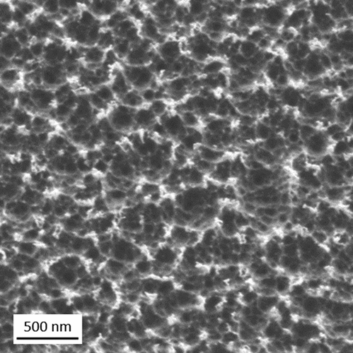
Figure 6. Effect of low-pressure oxygen plasma etching on polymers: Before and after comparison of the treated surface (SEM image).
The treatment duration with low-pressure plasma for pattern generation is not strictly constrained. Prolonged treatment durations primarily result in increased material removal, as a consistent etching rate is maintained.[Citation24] However, the resulting pattern structure remains largely similar. In this study, the identical parameters for the plasma process were used for generating the patterns as those used for pretreating the surfaces of the joining parts before bonding (refer to section 2.2).
Damage to the test specimen due to low-pressure plasma treatment, which could affect its mechanical properties in the ENF test, can be ruled out. This method represents a well-established technique for surface pretreatment of polymers, where maximum temperatures of 50°C are attained.[Citation13]
3.2. Testing procedure inside the SEM
To introduce shear load into the adhesive bondline, three-point bending tests are performed on one-sided notched test specimens. A tension-compression module is utilized which has been expanded with an adapter specifically designed for bending tests. The bearings diameter is 4 mm with a separation distance of 20 mm. The entire test device fits into the vacuum chamber of the SEM and is externally controlled through a data line flange.
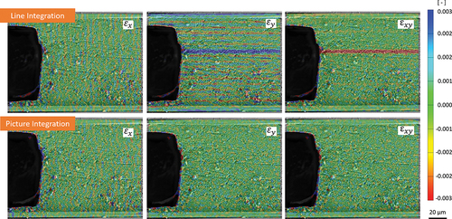
The way in which the SEM image is acquired plays a substantial role for the subsequent application of digital image correlation. Achieving low-noise and high-resolution SEM images demands on appropriate beam scanning and SE detector information processing. It is crucial to ensure that no distortions arise in the image during the SEM acquisition. These could be incorrectly interpreted as strains on the specimens outside. To create SEM images, the SE beam must scan the sample several times. The signal from the SE detector can be integrated either several times sequentially per line (Line Integration) or over entire images (Picture Integration). Line Integration typically provides sharper images but may introduce distortions, as illustrated in . However, these distortions do not occur with Picture Integration. Therefore, this integration method was selected for creating image series for DIC evaluations. An integration time of 30 s − 60 s was found to be reasonable for the examined samples at the selected magnifications, which spanned from approximately 250 µm to 160 µm in image width.
Figure 7. Distortions detected via DIC on two consecutively acquired SEM cross section images of an unloaded sample. Severe distortions due to image acquisition are visible with the line integration method, but not with picture integration.
However, this necessitates that continuous testing is not feasible for such prolonged periods. Consequently, the specimen must be loaded incrementally, and the test device has to be turned off each time an image is acquired. For the ENF specimens, the applied load has ranged from 0 N to failure at a maximum of −800 N. A step size of −100 N was determined to be a favorable compromise solution in terms of time and experimental benefits.
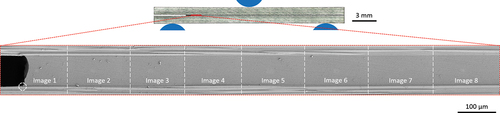
While a SEM can provide highly detailed and high-resolution close-up images of a sample, it is also limited to higher magnifications. Consequently, capturing larger areas of the sample requires stitching of single images. Therefore, for the examination of adhesive layers, the microscope stage is successively moved sideways together with the tension-compression module and an image is acquired at each position step. An overlap of the images of approximately 10% on each side is aimed for. These single images can then be stitched together into one image, which was done manually using the open source software GIMP. Afterwards the images are stacked and aligned on the lower joining part where the artificial crack ends (see white circle in ). Subsequently, the images are cropped to the relevant area around the adhesive layer. A composed high-resolution image of the adhesive layer, including a size comparison to the entire sample, is presented in . It is important for the acquisition of all images across multiple load levels that the settings on the microscope remain unchanged. This ensures the creation of a valid database for subsequent evaluation with DIC.
Figure 8. Side view of an ENF sample (top) with a detailed view of the adhesive layer and the relevant area for image evaluation (bottom). The lower image shows a high-resolution image composition consisting of 8 SEM cross section images with a total of 14,051 x 1377 pixels.
3.3. DIC analysis
The SEM images are analyzed using the DIC software GOM Correlate Pro. In the initial step importing the images and creating a surface component is involved. This requires defining the size of the facets, which combine multiple pixels into one gray value. As facet size increases, the stability of the evaluation improves, but accuracy decreases. Therefore, a suitable balance must be chosen. For the evaluation of the adhesive layers, a facet size of 27 pixels and a point distance of the facets of 17 pixels were chosen based on preliminary tests. The calculation was performed in “standard” mode.
4. Results and discussion
In the following section, we present selected representative examples of strain distributions determined from SEM images of bonded specimens with various geometries. It is observed that pattern recognition exhibits less stability on the fibers compared to the adhesive or resin. This is attributed to a reduced structuring effect of the etching process on the fibers. On polymers such as the adhesive or resin of the CFRP, however, pattern recognition performs very effectively and reliably.
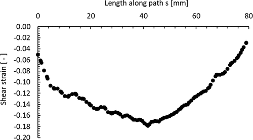
The initial and simplest case under consideration involves a bond comprising two joining parts with flat topography, fabricated using a release film. In , the shear strain distribution in this adhesive layer is depicted at a load of −400 N. This illustrates the method’s capability to capture detailed strain information. Notably, on the left side of the center, a minor delamination has occurred on the lower joining part, visibly influencing the strain distribution. A clear progression of the strain magnitude over the adhesive layer thickness can be seen, with a maximum in the center of the bondline and a decrease in strain towards the edges of the adhesive layer. Detailed views of these regions can be seen in . presents the quantitative evaluation of the shear strain along the path s marked in .
Figure 9. SEM cross section image overlaid with DIC calculation of shear strains in an adhesive layer with plain joining parts at −400 N. On the lower joining part, to the left of the center, the influence of a small delamination on the strain distribution is visible.
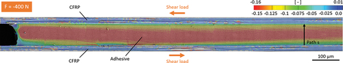
Figure 10. Detailed views of the strain distribution shown in : (a) End of the artificial crack. (b) Delamination, marked with an ellipse. (c) Progression of the strain magnitude over the adhesive layer thickness.
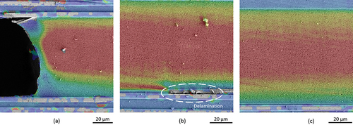
Figure 11. Shear strain across the cross section of the adhesive layer along the path s shown in .
In , the shear strain distribution of a specimen with distinctly structured CFRP joining parts at −300 N, −400 N and −500 N compressive load is illustrated. The use of peel ply in the CFRP manufacturing process has led to a textured surface characterized by resin-rich regions. Since the DIC pattern can be generated directly on the specimen’s surface without additional layers, the actual surface of the specimen is visible throughout. This allows a good differentiation between various areas of the specimen such as adhesive and resin. The images demonstrate the pronounced impact of the topography of the joining parts on the strain within the adhesive layer.
Figure 12. SEM cross section image overlaid with DIC calculation of shear strains in an adhesive layer with structured joining parts at −300 N (top), −400 N (middle) and −500 N (bottom). The distribution of strain is influenced by the structure of the joining parts.
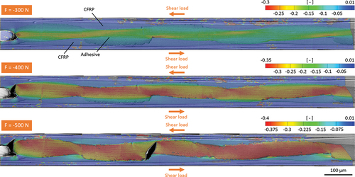
Under a −500 N load, the development of a crack in the adhesive layer induces a notable alteration in the strain distribution. Consequently, the load is redirected to regions that were previously subjected to lower stress. The presented methodology enables a comprehensive quantification of this process.
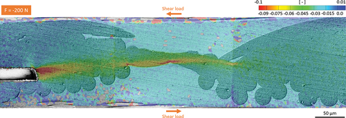
When examining a specimen with a significantly thinner adhesive layer, the formation of shear bands can be visualized. shows the localization of strains in a narrow band in the adhesive layer. The magnification of the region around the tip of the insert at a load level of −200 N is illustrated in , demonstrating the high spatial resolution achievable with this method.
Figure 13. SEM cross section image overlaid with DIC calculation of shear strains in an adhesive layer with structured joining parts at −300 N with visible formation of shear bands.
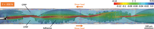
Figure 14. Magnification of the shear strains at −200 N in the vicinity of the insert tip.
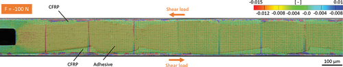
For specimens experiencing low load levels, selecting a very narrow legend scaling can reveal artifacts arising from the SEM image acquisition and composition, as illustrated in . Particularly in the areas where images were stitched together, vertical lines with varying measurement values may appear. A correlation within individual image series and subsequently stitching the results is not feasible, as the test specimen undergoes significant deformation relative to the image frame, leading to its displacement from the image area. However, since this effect occurs only locally and is clearly identifiable, this does not pose a serious concern in the interpretation of the results. In addition, slight pattern-like inhomogeneities can be seen that are due to the scanning nature of the image generation, but this is only the case at very high gains of the strain display colors. Artifacts such as those mentioned above can be reliably distinguished from the specimen’s mechanical information, as they are easily identifiable, often exhibiting periodic repetition. However, discerning potential unknown artifacts from the measured data is not feasible.
Figure 15. SEM cross section image overlaid with DIC calculation of shear strains in an adhesive layer at −100 N. Due to the narrow scaling of the legend with respect to the range of values, vertical lines appear as artifacts of the image composition from single images.
A methodological constraint that necessitates constant consideration during result interpretation is the inherent limitation of solely observing the surface of the sample. Consequently, no statements can be made about the stress and strain state inside the specimen. For example, it is conceivable that micro-damage can occur inside the specimen without this being visible on the outside.
Since stereo images cannot be recorded with an SEM, potential measurement errors may arise due to a backward movement of the specimen. Such errors could erroneously indicate a reduction in the specimen size. Nevertheless, the implementation of a robust test fixture design and the secure stabilization of the specimen significantly mitigate the likelihood of such inaccuracies.
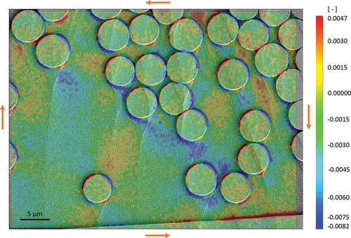
It is noteworthy that this methodology is not limited to the scale of adhesive bondlines and can be effectively applied to different scales. To demonstrate its versatility and robustness across various scales, down to the upper nanometer range, an example of the fiber-matrix interface in CFRP laminate is given here. illustrates the shear strain of the matrix around the carbon fibers under mixed shear and compression loading induced by three-point bending. The specimen preparation involved the use of an ion beam cross section polisher (Ion Milling System ArBlade 5000, Hitachi Ltd., Tokyo, Japan), a crucial step for achieving a clean cut through materials of varying hardness. The advantages of this method for SEM imaging have been previously demonstrated by Holtmannspötter et al..[Citation16] For this load case, it can be observed that the highest distortions occur in the resin between adjacent fibers, particularly in the region of the fiber-matrix interface.
Figure 16. SEM cross section image overlaid with DIC calculation of shear strain distribution in a CFRP laminate subjected to bending load.
The results shown above were chosen to give an overview of the microstructure of the material, but the image correlation also works at higher magnifications. The maximum resolution depends on the microscope used and the quality of the chamber vacuum. At very high magnifications, however, the method is constrained by the stiffness of the materials under investigation. If the observed deformations are too small, the distortions induced by the SEM, such as drift, predominate. A meaningful evaluation is then no longer feasible.
5. Conclusion
A novel method for quantitative micro- and nanometer-scale measurements of loaded ENF specimens inside a SEM has been developed and demonstrated in this work. In our approach, images from a field emission SEM are evaluated using image correlation algorithms. The presented method, which employs an etching process to create a speckle pattern, is particularly well-suited for polymers. This enables the investigation of bondings on a scale that allows thin adhesive layers to be imaged under load with very high resolution for the first time, taking into account the relevant scale at which mechanical processes occur. The method has demonstrated stability, allowing for the observation of micro-damage, strain distribution, and the formation of shear bands in adhesive layers. The measured shear strains appear plausible as they fall within a technically feasible range and exhibit consistency across multiple specimens.
A limitation of the method is the high time expenditure, both in the testing procedure and in the post processing of the individual images. However, the knowledge gained per sample is substantial, necessitating the examination of only a few samples to understand the mechanisms occurring at the micrometer scale. This stands in contrast to the exclusive use of coupon specimens, where effects can only be measured in a superimposed manner, usually requiring the testing of a large number of specimens.
Future plans involve systematic investigations of bonded joints with different joint geometries and fillers using this method. In addition to pure shear loading, other loading modes are of interest. With a small modification, the described specimens can be tested in the fixture as single-leg bending specimens, allowing for the investigation of a mixed-mode loading condition for continuative interfacial fracture toughness testing.[Citation25]
Disclosure statement
No potential conflict of interest was reported by the author(s).
Additional information
Funding
References
- Irving, P. E., ed. Polymer Composites in the Aerospace Industry; Woodhead Publishing: Amsterdam, Heidelberg, 2015.
- Banea, M. D.; Da Silva, L. F. M. Adhesively Bonded Joints in Composite Materials: An Overview. Proc. Inst. Mech. Eng. Part L J Mater. Des. Appl. 2009, 223(1), 1–18. DOI: 10.1243/14644207JMDA219.
- Budhe, S.; Banea, M. D.; de, B. S.; Da Silva, L. An Updated Review of Adhesively Bonded Joints in Composite Materials. Int. J. Adhes. Adhes. 2017, 72, 30–42. DOI: 10.1016/j.ijadhadh.2016.10.010.
- Hild, F.; Roux, S. Digital Image Correlation: From Displacement Measurement to Identification of Elastic Properties - a Review. Strain 2006, 42(2), 69–80. DOI: 10.1111/j.1475-1305.2006.00258.x.
- Oshima, S.; Yoshimura, A.; Hirano, Y.; Ogasawara, T.; Tan, K.-T. In-situ Observation of Microscopic Damage in Adhesively Bonded CFRP Joints Under Mode I and Mode II Loading. Compos. Struct. 2019, 227, 111330. DOI: 10.1016/j.compstruct.2019.111330.
- Thäsler, T.; Holtmannspötter, J.; Gudladt, H.-J. Monitoring the Fatigue Crack Growth Behavior of Composite Joints Using in situ 2D-Digital Image Correlation. J. Adhes. 2019, 95(5–7), 595–613. DOI: 10.1080/00218464.2018.1562923.
- Janeliukstis, R.; Chen, X. Review of Digital Image Correlation Application to Large-Scale Composite Structure Testing. Compos. Struct. 2021, 271, 114143. DOI: 10.1016/j.compstruct.2021.114143.
- Kammers, A. D.; Daly, S. Digital Image Correlation Under Scanning Electron Microscopy: Methodology and Validation. Exp. Mech. 2013, 53(9), 1743–1761. DOI: 10.1007/s11340-013-9782-x.
- Chai, H. Shear Fracture. Int. J. Fract 1988, 37(2), 137–159. DOI: 10.1007/BF00041716.
- Hexcel Corporation. HexPly 8552; Product Data Sheet: Stamford, CT, USA, 2023.
- Henkel Corporation Aerospace. Technical Process Bulletin LOCTITE EA 9396 AERO, 7th ed.; Bay Point, CA, USA, 2013.
- Holtmannspötter, J. How Surfaces of Carbon Fiber Reinforced Plastics with Thermoset Matrices Need to be Treated for Structural Adhesive Bonding. J. Adhes. 2020, 96(9), 839–854. DOI: 10.1080/00218464.2018.1519702.
- Arikan, E.; Holtmannspötter, J.; Zimmer, F.; Hofmann, T.; Gudladt, H.-J. The Role of Chemical Surface Modification for Structural Adhesive Bonding on Polymers - Washability of Chemical Functionalization Without Reducing Adhesion. Int. J. Adhes. Adhes. 2019, 95, 102409. DOI: 10.1016/j.ijadhadh.2019.102409.
- Handbuch Klebtechnik, R. M. München; Hanser: Wien, 2012.
- Henkel. Technical Data Sheet LOCTITE FREKOTE 55-NC; Düsseldorf, Germany, 2017.
- Holtmannspötter, J.; Wetzel, M.; von, C. J.; Brucksch, R. Ultra High-Resolution Imaging of Interface Layers. Adhes. Adhes. Sealants. 2013, 10(4), 22–27. DOI: 10.1365/s35784-013-0233-y.
- Ackermann, J. Handbuch für die Rasterelektronenmikroskope SUPRA(VP) und ULTRA; Oberkochen, Germany, 2004.
- Jin, H.; Lu, W.-Y.; Korellis, J. Micro-Scale Deformation Measurement Using the Digital Image Correlation Technique and Scanning Electron Microscope Imaging. J. Strain Anal. Eng. Des. 2008, 43(8), 719–728. DOI: 10.1243/03093247JSA412.
- Wachi, Y.; Koyanagi, J.; Arikawa, S.; Yoneyama, S. In situ SEM Deformation Behavior Observation at CFRP Fiber-Matrix Interface. In Composite, Hybrid, and Multifunctional Materials, Tandon, G., Ed.; Springer International Publishing: Cham, 2015; Vol. 4, pp. 67–73.
- Yin, Y.; Xie, H.; He, W. In situ SEM-DIC Technique and Its Application to Characterize the High-Temperature Fatigue Crack Closure Effect. Sci. China Technol. Sci. 2020, 63(2), 265–276. DOI: 10.1007/s11431-018-9477-6.
- Hoefnagels, J.; van Maris, M.; Vermeij, T. One-Step Deposition of Nano-To-Micron-Scalable, High-Quality Digital Image Correlation Patterns for High-Strain in-situ Multi-Microscopy Testing. Strain. 2019, 55(6), e12330. DOI: 10.1111/str.12330.
- Mammadi, Y.; Joseph, A.; Joulain, A.; Bonneville, J.; Tromas, C.; Hedan, S.; Valle, V. Nanometric Metrology by FIB-SEM-DIC Measurements of Strain Field and Fracture Separation on Composite Metallic Material. Mater. Des. 2020, 192, 108665. DOI: 10.1016/j.matdes.2020.108665.
- Carter, J. L. W.; Uchic, M. D.; Mills, M. J. Impact of Speckle Pattern Parameters on DIC Strain Resolution Calculated from in-situ SEM Experiments. In Fracture, Fatigue, Failure, and Damage Evolution; Carroll, J., Daly, S., Eds.; Conference Proceedings of the Society for Experimental Mechanics Series. Springer, Cham, 2015; Vol. 5. DOI: 10.1007/978-3-319-06977-7_16.
- Lake, M. Oberflächentechnik in der Kunststoffverarbeitung: Vorbehandeln, Beschichten, Funktionalisieren und Kennzeichnen von Kunststoffoberflächen; Hanser: München, 2009.
- Davidson, B. D.; Sundararaman, V. A Single Leg Bending Test for Interfacial Fracture Toughness Determination. Int. J. Fract. 1996, 78(2), 193–210. DOI: 10.1007/BF00034525.