
Abstract
The gas electron multiplier (GEM) is a gaseous detector that is widely used in many applications. Our glass GEM (G-GEM) comprises a photo-etchable glass (PEG3, HOYA Corporation, Japan). Our research indicated that it shows superior performance compared with other gas detectors. In this article, a new type of G-GEM is introduced. It has a guard-ring structure around the holes in order to improve the spark tolerance by reducing the total capacitance of each hole structure. A measured gas gain of approximately 7500 is attained for this new G-GEM with a single-sided guard-ring structure using a gas mixture of Ar (90%) and CH4 (10%) in the gas flow mode. An energy resolution of 17.3% (FWHM) is also achieved with a collimated 6 keV X-ray beam. The results of a 10 to 12 hour gas gain stability measurements are also shown.
1. Introduction
1.1. Development of G-GEM
The gas electron multiplier (GEM) is one of the most widely used micropattern gaseous detectors (MPGD) [Citation1] and is applied in a variety of fields including high-energy physics [Citation2,3], neutron scattering experiments [Citation4], and medical imaging. The GEM is composed of a thin polyimide insulator, which is sandwiched between thin copper foils. The typical thickness of the GEM is approximately 50 μm. Numerous minute holes are fabricated over the entire surface. High voltages (HV) are applied to the copper foil electrodes, generating a high electric field inside each hole. Thus, each hole of the GEM works as an individual proportional counter. The GEM exhibits superior performance in terms of its high gas gain, high count rate capability, and high position resolution. GEMs have attracted much attention since they were introduced in 1997. Since then, a variety of GEM-derived detectors, including GEMs with different materials, geometries, and fabrication processes have been reported [Citation5].
When used in a multi-stage mode, GEMs such as the double-GEM or triple-GEM can achieve a very high overall gas gain. However, for the simplicity of the setup, it is preferable to use a single GEM to achieve very high gas gains. In this respect, thick alternative substrates have been considered because they have longer amplifying regions than the thin polyimide foils of a standard GEM. A thick GEM (THGEM) with a high gas gain in a single-THGEM mode was developed [Citation6] for this purpose.
We recently developed a new type of micropattern gaseous detector called glass GEM (G-GEM) [Citation7] (). The G-GEM's substrate is composed of photo-etchable glass (PEG3, HOYA Corporation, Japan [Citation8]). The thickness of the substrates is between 300 and 700 μm, which is much thicker than the 50 μm thickness of a standard GEM. Since the substrate of a G-GEM is composed of a photo-etchable glass, holes can be accurately formed using a photolithography technique to achieve good hole size uniformity over the entire sensitive area. The G-GEM's glass substrate is solid and self-supporting. Thus, it provides better handling and a simple detector structure. In addition, the substrate is composed of inorganic materials, and it is completely free of outgas. Therefore, the G-GEM is very promising for applications requiring sealed-type detectors. We have developed several types of G-GEMs with different geometries and electrode materials that exhibit superior performances in terms of high gas gains and high-energy resolutions. The highest gain we achieved was 6700, and the best energy resolution was 18.8% (FWHM), for uniform irradiation from an 55Fe source. The X-ray image was also successfully obtained using a charge division method. Those results were reported in [Citation7].
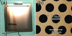
Figure 1. (a) Photograph of a G-GEM and (b) magnified photograph of the holes. The hole diameter and pitch is 170 and 280 μm, respectively.
1.2. Spark tolerance of GEM
Although GEMs are widely used, its spark tolerance is still an important issue that needs to be resolved. GEMs will break down when huge sparks occur. The electrostatic capacitance of a GEM is very large because it is composed of a thin dielectric substrate sandwiched between metal layers. Hence, a lot of electric charges accumulate on the capacitance. If sparks occur inside a hole of the GEM, a huge amount of charge flows into the hole and causes severe damage to the hole and surfaces of the GEM. Therefore, solutions for improving the GEM spark tolerance are required, and a few ideas have been reported. For example, Bachmann et al. proposed a segmentation approach to divide the surface electrodes of standard GEMs into sections [Citation9]. A rim structure around each hole of THGEM was also proposed to suppress the sparks [Citation10].
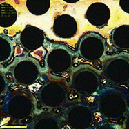
G-GEM can also be heavily damaged by sparks. As mentioned before, G-GEM is composed of a glass substrate, and electrodes are coated on both sides of the glass substrate. A typical electrode is composed of two metal layers: a chromium layer on the glass and a copper layer on the chromium layer. The glass is a spark tolerant material; therefore, the substrate itself is not too heavily damaged by sparks. However, the metal layers will melt or evaporate because of huge and consecutive sparks, which can cause severe damage. is a photograph of the G-GEM, the metal layers of which were melted or blown away by sparks.
Figure 2. A photograph of G-GEM, the metal part of which is heavily damaged by sparks.
2. A new solution: guard ring
We are trying to develop a new approach for improving the spark tolerance of G-GEMs by equipping each hole with a surrounding metal ring. We call this metal ring a “guard ring”. is a photo of the guard-ring structure. The guard rings were made using a laser etching technique after fabricating the normal hole structure.
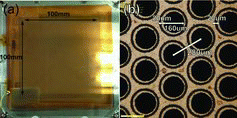
Figure 3. (a) Photograph of the G-GEM guard ring. The sensitive area is 100 mm × 100 mm. (b) A magnified photograph of the holes. The guard-ring width, gap between the ring and hole, hole diameter, and hole pitch are 20, 20, 160, and 280 μm, respectively.
In a normal electrode structure without guard rings, a large amount of electric charge accumulates. The amount of charge released by a spark can induce damage to the surface metals or holes.
There are two main purposes of the guard ring that protects the hole from the spark damage. One is to reduce the capacitance around each hole, thereby reducing the amount of charge that accumulates on the metal. The other is to decouple the hole from an HV supply by inserting a series resistance between the HV supply and GEM hole, which can work as a voltage drop element whenever a large current flows into the GEM hole. The surface of each guard ring is considerably small; hence, the amount of charge on a ring is small, resulting in less spark charge and damage.
3. Electric field calculation
Before fabricating the single-sided guard-ring structure, we performed the calculations on the electric field inside the hole and compared the results with the conventional structure. The results showed that the single-sided guard-ring structure can achieve a high gas gain.
3.1. The method of calculation
We used the ELFIN calculation code, which was developed by the ELF Corporation, Japan [Citation11]. ELFIN uses the “Integrated Element Method,” which was originally developed by ELF Corporation, to calculate the electric field. If we choose the Finite Element Method (FEM) for the field calculations, we have to make a precise calculation model to obtain a precise result. In that case, we have to pay much attention in making the fine mesh structure, which will require an immense amount of time and effort. Conversely, ELFIN's integrated element method produces the calculated results with great accuracy, despite the mesh size. Therefore, we can effectively develop calculation models using ELFIN.
3.2. Calculation model and setup
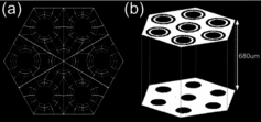
First, we made a calculation model that represented the holes of the G-GEM with a guard-ring structure. A schematic view of the model from two different angles is shown in . We made a total of seven holes in the model, and calculated the electric field that formed inside the center hole. The geometry is the same as the actual G-GEM used for the subsequent experiments.
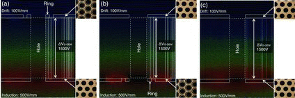
Figure 4. The calculation model from the (a) top view and (b) view from a different angle. The guard-ring structure is created only on a single side. The ring width, gap between the ring and hole, hole diameter, hole pitch, and thickness of the glass substrate, are 20, 20, 160, 280, and 680 μm, respectively. The dielectric constant is 6.28 for the PEG3 glass.
We designed two different calculation setups using the model shown in . The difference between the two setups is the location of the guard ring surface: it is on the topside in one setup and on the backside in the other setup. In other words, the common model is used, but it is placed upside down in the two setups.
The voltages of the topside and backside of the G-GEM are 1000 and 2500 V, respectively. Hence, the voltage difference between the top and back (ΔVG-GEM) is 1500 V. The cathode electrode is placed 10 mm above the G-GEM, and the field between the cathode and G-GEM topside is 100 V/mm (drift field). The anode electrode is placed 2 mm below the G-GEM, and the field is 500 V/mm (induction field).
3.3. Calculation result
We calculated the electric field that formed inside the center hole of the model at each setup. shows the results. The guard ring is not directly connected to the power supply, and the potential of the guard ring is determined by the surface and bulk resistance of the substrate. The potential of the ring is determined along the potential formed by the voltage applied to the electrodes at the topside and backside. As a result of the calculations, we found that similarly strong field was formed with this guard ring G-GEM, compared with the normal G-GEM without the guard ring. We therefore expect high gas gain characteristics with this guard ring G-GEM.
Figure 5. The electric field calculation setup in which the guard-ring surface is on the (a) topside and (b) backside. (c) is the normal G-GEM (no guard ring) as a reference. With each setup (a) and (b), we can see that a high electric field forms inside the center G-GEM hole. The colored lines represent the equipotential lines. Red and blue lines indicate the high and low potentials, respectively. The high potentials are around the backside, and the low potentials are around the topside.
4. Experiment
4.1. Setup
We tested two different setups, which are shown in . We used the same 680-μm-thick G-GEM, which has the guard-ring structure only on a single surface. In one setup, the guard-ring surface was on the topside, while it was on the backside in the other setup. The other conditions are identical. We used a mixture of Ar (90%) and CH4 (10%) at atmospheric pressure in the gas flow mode. An 55Fe X-ray source was placed on the window, and the entire sensitive area was irradiated (uniform irradiation). We also tested the G-GEM with a collimated 6 keV X-ray beam from the synchrotron at the KEK photon factory in Japan. The beam size was 60 μm by 60 μm. The high voltages were independently supplied to the anode electrode as well as the G-GEM topside and backside. The drift field was 100 V/mm, and the induction field was 500 V/mm.
Figure 6. The guard-ring surface on the (a) topside and (b) backside.
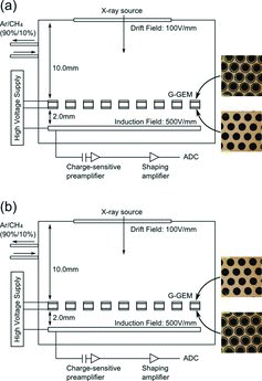
The readout anode electrode was a single planar electrode connected to a charge-sensitive preamplifier (CLEAR-PULSE CS515-1 [Citation12]). The charge pulses induced at the anode are read by the preamplifier and converted to voltage signals. Those signals are then filtered through a general purpose shaping amplifier, and recorded by a multi-channel spectrum analyzer (Fast Comtec MPA-3 [Citation13]).
We tested several fundamental characteristics of the G-GEM guard ring, including the gas gain, energy resolution, long-term gas gain stability, and gas gain uniformity along the surface of the G-GEM.
4.2. Gas gain
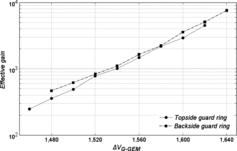
shows the gas gain curves obtained from both setups. Using both setups, we achieved a high gas gain of 4500 and 7500 for the topside and backside rings, respectively. The similar gas gain curves were observed between the topside and the backside ring structure.
Figure 7. The gain curve of the topside (circles) and backside (squares) guard-ring setup. The horizontal axis is the applied voltage between the G-GEM topside and backside. The vertical axis is the effective gas gain.
4.3. Energy resolution
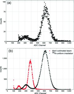
We investigated the energy resolution of the G-GEM with a uniform irradiation from an 55Fe 5.9 keV X-ray source and a collimated 6 keV X-ray beam from the synchrotron at KEK. shows the results. is the topside guard-ring setup, while is the backside guard-ring setup. We achieved an energy resolution of 22.4% (FWHM) for the topside ring setup and 23.4% (FWHM) for the backside ring setup using the 55Fe uniform irradiation. Meanwhile, an energy resolution of 17.3% (FWHM) was obtained by irradiating the backside ring setup with the collimated 6 keV X-ray beam from the synchrotron. We believe that the holes were created with good uniformity through photolithography and that the variation in the electric fields was small because we were able to obtain a good energy resolution even with the uniform irradiation, not only with the collimated beam.
Figure 8. (a) Topside guard-ring setup showing the energy spectrum of the 55Fe uniform irradiation. The energy resolution was 22.4% (FWHM) at a gain of approximately 1480. (b) Backside ring setup showing the 60 μm square collimated beam (red circles) and 55Fe uniform irradiation (black x-marks). The resolutions were 17.3 and 23.4% (FWHM) at gains of approximately 2700 and 6300, respectively.
4.4. Long-term stability
For applications that require long-term operations of the detector system, it is important for the detector to be stable for a long time. As a result, we tested the stability of the gas gain of the guard ring G-GEM. The results are shown in . show the topside and backside guard-ring setup, respectively. For each setup, the gas gain decreased by approximately 20 to 25% from the beginning of the operation. We found that the gain stabilities are different between topside ring and backside ring. For the topside ring, the gain saturated after about eight hours of operation. On the other hand, for the backside ring, it did not. The exact reason for this tendency is still under investigation.
Figure 9. The gas gain of the (a) topside and (b) backside guard ring during the period between 10 to 12 h from the start of the test. The case (a) was tested with 55Fe source (about 164 kBq), and the case (b) was tested using a collimated beam (850 cps at 60 μm square area).
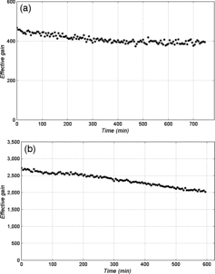
If a conventional GEM is used, the gain continues to increase by the charge-up effect [Citation5,Citation14]. However with this guard ring G-GEM, we did not observe the gain increase, because of its low charge-up property by the low resistivity of PEG3.
4.5. Gas gain uniformity
We have tested the gas gain uniformity using a collimated 6 keV square X-ray beam from the synchrotron at KEK. The beam size was 60 μm square. We could only test the backside ring setup during the allowed beam time. In this uniformity test, the detector chamber was moved in 10 mm steps using an X–Z stage controller. At each point, the gas gain was investigated. We moved the chamber 10 times in each direction and scanned a 100 mm by 100 mm area. The results are shown in . The normalized gas gain is shown in each grid point.
Figure 10. The gain uniformity of the guard ring G-GEM.
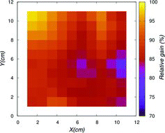
The gas gain at each point was normalized to the highest gas gain. The numerical value of the highest gain was 5700. The lowest relative gain was found at the right side of the G-GEM, which was approximately 74%. The highest gain was obtained at the top left corner. Although the gain variation was supposed to be randomly distributed over the entire G-GEM, the results showed that only a specific region had low gas gain. Currently, we believe that the induction field, which had a relatively large effect on the gas gain, was lower near the right side (low gain part) compared with the other side, which showed a higher gas gain.
5. Conclusion
In this research, we developed a new guard-ring G-GEM and investigated its basic characteristics as a gaseous detector. It exhibited a high gas gain up to 7500. The energy resolution was 22.4% (FWHM) with the 55Fe 5.9 keV X-ray uniform irradiation, and reached 17.3% (FWHM) with the collimated 6 keV X-ray beam from the synchrotron at KEK. For the long-term stability test, the gas gain decreased by approximately 20 to 25% from the beginning of the operation for each setup. The gas gain uniformity was also tested. In conclusion, we have confirmed that the new G-GEM works properly and exhibits a good performance.
References
- Sauli F. GEM: a new concept for electron amplification in gas detectors. Nucl Instr Meth A. 1997;386:531–534.
- Ketzer B, Weitzel Q, Paul S, Sauli F, Ropelewski L. Performance of triple GEM tracking detectors in the COMPASS experiment. Nucl Instr Meth A. 2004;535:314–318.
- Sharma A. Muon tracking and triggering with gaseous detectors and some applications. Nucl Instr Meth A. 2012;666:98–129.
- Ohshita H, Uno S, Otomo T, Koike T, Murakami T, Satoh S, Sekimoto M, Uchida T. Development of a neutron detector with a GEM. Nucl Instr Meth A. 2010;623:126–128.
- Tamagawa T, Hayato A, Asami F, Abe K, Iwamoto S, Nakamura S, Harayama A, Iwahashi T, Konami S, Hamagaki H, Yamaguchi YL, Tawara H, Makishima K. Development of thick-foil and fine-pitch GEMs with a laser etching technique. Nucl Instr Meth A. 2009;608:390–396.
- Chechik R, Breskin A, Shalem C, Mörmann D. Thick GEM-like hole multipliers: properties and possible applications. Nucl Instr Meth A. 2004;535:303–308.
- Takahashi H, Mitsuya Y, Fujiwara T, Fushie T. Development of a glass GEM. Nucl Instr Meth A. 2013;724:1–4.
- http://www.hoyaoptics.com/gcb/index.htm
- Bachmann S, Bressan A, Capeans M, Deutel M, Kappler S, Ketzer B, Polouektov A, Ropelewski L, Sauli F, Schulte E, Shekhtman L, Sokolov A. Discharge studies and prevention in the gas electron multiplier (GEM). Nucl Instr Meth A. 2002;479:294–308.
- Chechik R, Breskin A, Shalem C. Thick GEM-like multipliers—a simple solution for large area UV-RICH detectors. Nucl Instr Meth A. 2005;553:35–40.
- http://www.elf.co.jp/
- http://www.clearpulse.co.jp/jpn/product/plist_B/plistB3.html
- http://www.fastcomtec.com/products/multichannel-analyzers.html
- Simon F, Azmoun B, Becker U, Burns L, Crary D, Kearney K, Keeler G, Majka R, Paton K, Saini G, Smirnov N, Surrow B, and Woody C. Development of tracking detectors with industrially produced GEM foils. IEEE Trans Nucl Sci. 2007;54:2646–2652.