
 ?Mathematical formulae have been encoded as MathML and are displayed in this HTML version using MathJax in order to improve their display. Uncheck the box to turn MathJax off. This feature requires Javascript. Click on a formula to zoom.
Abstract
Secondary cosmic-ray neutron-induced soft errors in an n-type metal-oxide-semiconductor field-effect transistor are analyzed based on the multiple sensitive volume (MSV) model using Particle and Heavy Ion Transport code System (PHITS). The soft error rates (SERs) and the collected charge for each single event are compared with those obtained by PHits-HYenexss integrated code System for Effects of Radiation on Device (PHYSERD) based on the detailed technology computer-aided design (TCAD) simulation and by the single sensitive volume (SSV) model using PHITS. It is found that PHITS+MSV provides approximate SERs in a shorter time than PHYSERD by estimating collected charges without event-by-event TCAD simulation. Furthermore, PHITS+MSV reproduces collected charge for each single event more accurately than PHITS+SSV by considering spatial dependence of the charge collection efficiencies. Therefore, PHITS+MSV is the most suitable to estimate SERs in practical design of semiconductor devices which require high accuracy and a short computational time.
1. Introduction
Radiation-induced temporary and non-destructive faults (the so-called soft errors) have been recognized as a serious problem affecting the reliability of microelectronic devices. Charged particles entering from outside a semiconductor device or generated via a nuclear reaction inside the device create electron–hole pairs along their tracks. Some of the created charges are collected in the storage node of a memory element such as a static random-access memory by drift and diffusion, and there is a possibility to upset the stored data (the so-called single event upset or SEU). In order to ensure long-term stable system operation or normal operation in a harsh radiation environment, measures must be taken to prevent soft errors in devices. Physics-based simulation of soft errors is helpful for the research and development of radiation-tolerant devices because it can predict soft error rates (SERs) in the design stage of devices and circuits. Several Monte Carlo-based simulation tools have been developed [Citation1–3], including our developed multi-scale Monte Carlo simulator called PHits-HYenexss integrated code System for Effects of Radiation on Devices (PHYSERD) [Citation4–6]. PHYSERD consists of the particle transport code PHITS (Particle and Heavy Ion Transport code System) [Citation7] and the three-dimensional (3D) technology computer-aided design (TCAD) simulator Hyper Environment for Exploration of Semiconductor Simulation (HyENEXSS) [Citation8]. It has been applied to analysis of neutron-induced soft errors based on event-by-event TCAD simulation, which simulates the process and the transient response of semiconductor devices [Citation4–Citation6,Citation9,Citation10].
Although such a physics-based simulation method is powerful and reliable, it is not suitable for estimation of SERs in particular situations (e.g., to optimize memory layout, to validate the tolerance of a device in different radiation environments) because TCAD simulation is time consuming. A sensitive volume (SV) model [Citation11] has been commonly employed to estimate the amount of charges collected in storage node without TCAD simulation. Two types of SV models exist: the single-SV (SSV) model and the multiple-SV (MSV) model [Citation12]. The SSV model assumes that all charges deposited in the SV are collected in the storage node. In contrast, the MSV model considers spatial dependence of the charge collection efficiency (CCE) which is defined as the ratio of deposited charge to collected charge. The shape, size and CCE of each SV are determined from linear energy transfer dependence of SEU cross sections obtained by heavy-ion testing [Citation13] and/or from results of detailed TCAD simulations. Numerous comparisons between calculated SERs with SV model and measured SERs have been reported [Citation11–16]. However, investigations of reproducibility of the collected charge for each single event are insufficient.
In order to reduce the computational time required to estimate SERs with PHITS, we had substituted the SSV model for HyENEXSS [Citation17]. However, it was found that the SSV model cannot estimate the collected charge for each single event obtained by the TCAD simulation, even though it can reproduce the SERs superficially. In the present work, the MSV model is adopted instead of the SSV model to reduce the computational time and to improve the reproducibility of collected charge for each single event. Secondary cosmic-ray neutron-induced soft errors in a 25-nm bulk-design rule n-type metal-oxide-semiconductor field-effect transistor (NMOSFET) are calculated by PHITS+MSV. The results are compared with those obtained by PHYSERD [Citation5] and PHITS+SSV [Citation17] to quantitatively clarify the reproducibility for PHITS+MSV.
2. Systematic investigation for charge collection process
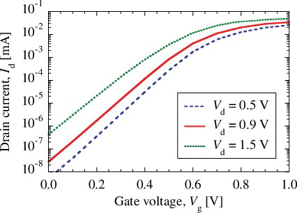
In order to determine the condition of MSV, charge collection process in the 25-nm design-rule NMOSFET was investigated by HyENEXSS systematically. illustrates the structural configuration of the NMOSFET. The NMOSFET parameters are listed in ; these parameters were also used in previous studies [Citation5,Citation6,Citation9] and are based on information given in [Citation18–20]. The doping profiles in the NMOSFET were fine-tuned to obtain a desired curve for drain current versus gate voltage (Id–Vg); see . Full 3D device simulations were made with default physical models implemented in HyENEXSS.
Figure 1. Configuration of the NMOSFET structure equivalent to 25-nm design rule used in HyENEXSS [Citation5,Citation6,Citation9]. STI (shallow trench isolation) prevents electrical current leakage between adjacent transistors, and active area is the area surrounded by STI.
![Figure 1. Configuration of the NMOSFET structure equivalent to 25-nm design rule used in HyENEXSS [Citation5,Citation6,Citation9]. STI (shallow trench isolation) prevents electrical current leakage between adjacent transistors, and active area is the area surrounded by STI.](/cms/asset/f2352f3d-42a3-47b1-a5f4-0c0871f3a504/tnst_a_1056561_f0001_oc.jpg)
Table 1. Parameters of NMOSFET for 25-nm design rule [Citation18–20].
Figure 2. Id–Vg curve for NMOSFET. In general, Id is sufficiently small at off-state of Vg. Id increases drastically together with Vg, and then increases moderately when Vg reaches a certain level.
The charge collection process is roughly classified into two types based on driving force, drift (whose driving force is the potential gradient) and diffusion (whose driving force is the concentration gradient). Therefore, the NMOSFET was first divided into two regions: one where the drift process dominates charge collection and another where the diffusion process plays the leading part of the charge collection. The drift process and the diffusion process were investigated separately, and the condition of MSVs was determined.
2.1. Drift process
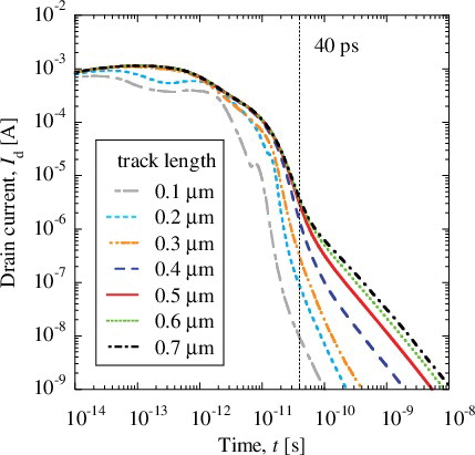
When an ion strikes the depletion region where charge carriers have diffused away and the electric potential gradient is formed, the potential inside the NMOSFET is temporarily distorted and it enhances charge collection by drift (the so-called funneling effect). As an example, shows snapshots of the temporal evolution of electron density, hole density and potential. At first, to verify the effective length for charge collection due to funneling, transient analyses were performed under the assumption that an ion strikes the center of drain node vertically. The hypothetical ion track had constant linear charge density of 10 fC/μm in a depth direction and a Gaussian radial distribution with a standard deviation of 30 nm, which roughly represents a He-ion track with the incident energy of 2 MeV. compares drain currents calculated with different ion-track lengths. Drain currents with an ion-track length exceeding 0.5 μm are almost identical up to about 40 ps, at which point the potential distortions disappear independent of ion-track length. This result indicates that the collected charge due to funneling is saturated, thus the effective funneling length is set to 0.5 μm.
Figure 3. Time evolution of electron density, hole density and potential for drain-node struck by ion with a track length of 0.1 μm. The potential is distorted along with the ion track, and reverts to normal at 43.1 ps. At 0.207 ps, electrons are pulled out from the source node to the substrate side.
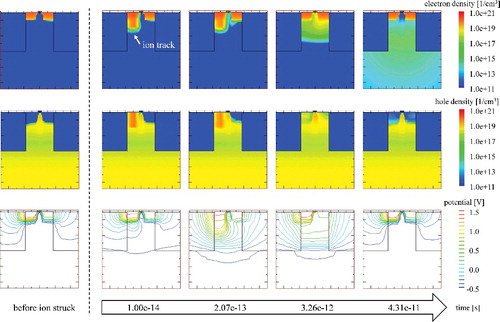
Figure 4. Drain currents in NMOSFET as a function of time and for various ion-track lengths.
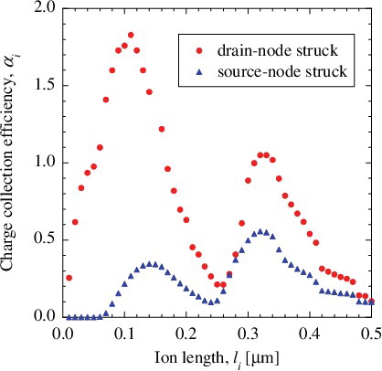
In order to obtain the CCE mainly due to drift, the transient analyses were performed with extending the length of the ion track. The CCE for ith position, αi, is defined by
(1)
(1) where Qdep(li) and Qcoll(li) are the deposited charge and the collected charge into drain node with an ion-track length of li, respectively. It is expected that most of the charges are collected into the source node when an ion strikes the depletion region on the source side. Therefore, CCEs were calculated not only for drain-node struck but also for source-node struck. shows these calculated CCEs. For drain-node struck, the CCEs with the ion-track length of around 0.1 μm exceed 1.0 because the distortion of potential pulls out additional electrons from the source node and they flow to the drain node, as shown in . This charge collection mechanism is called parasitic bipolar effect [Citation21]. The CCE decreases together with extending the length of ion track around 0.18 μm. It is probably caused that additional deposited charges impede the parasitic bipolar effect. For source-node struck, CCEs are lower than those for drain-node struck over the whole length. Especially below 0.06 μm, CCEs are nearly zero because almost all deposited charges are collected into the source node. Note that CCEs with the ion-track length of 0.5 μm are calculated for linear charge densities of several tens fC/μm which represent the heavy-ion tracks generated by secondary cosmic-ray neutrons. The difference of these CCEs was within 8%.
Figure 5. Charge collection efficiency for drain-node struck and source-node struck plotted as a function of ion-track length.
2.2. Diffusion process
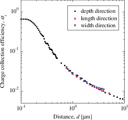
In order to investigate the CCE mainly due to diffusion, transient analyses with the spherical charge were performed. The spherical charge had almost the same charge density as that of the He-ion track with the maximum stopping power of 1.5 MeV/(g/cm2) and a Gaussian radial distribution with a standard deviation of 10 nm; as a result the amount of charge was 0.42 fC. The position of the spherical charge was varied in the transistor depth, length and width directions. Here, the CCE is given by the ratio of collected charge to deposited charge. shows the CCE plotted as a function of distance between the spherical charge and the center of transistor surface (i.e., the center of gate area). All CCEs plotted in are smaller than 1 because spherical charges were placed outside of the depletion region, and hence parasitic bipolar effect did not occur in any case. For the CCEs obtained by changing the position of charges vertically, they are almost constant below 0.15 μm because the deposited charge is near the depletion regions and is collected mainly by drift. After that, the CCE decreases with distance from the transistor surface. The CCEs obtained by laterally moving the charge in the depth of 0.75 μm from the transistor surface are almost the same as those obtained by varying the depth of the charge. This result indicates that spatial dependence of the CCE due to diffusion remains almost constant regardless of direction.
Figure 6. Charge collection efficiency for several positions of spherical charge plotted as a function of distance between spherical charge and center of transistor surface.
2.3. Condition of MSVs for NMOSFET
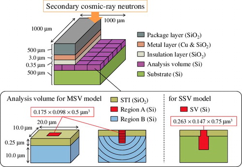
Based on the systematic investigation, the NMOSFET was divided into a region A where the CCE is mainly due to drift and a region B where the CCE is mainly due to diffusion. As shown in , region A is defined by the active area of the NMOSFET and an effective funneling length of 0.5 μm, and region B is defined as the rest of the NMOSFET. So as to keep the difference in CCEs of the two adjacent SVs below 10%, the region A was subdivided into 148 SVs and the region B was subdivided into 45 SVs. The CCE in the region A is switched event-by-event depending on whether ions strike in depletion regions because, as seen in and , they depend on the ion strike position. When an ion strikes both depletion regions, the average of the CCEs obtained by the drain-node struck and the source-node struck was applied.
Figure 7. Configuration of computational system used in PHITS. For the MSV model, the analysis volume is divided into regions A and B, which are then subdivided into smaller SVs. For the SSV model, an SV is placed on the analysis volume.
3. SER analysis based on MSV model
3.1. Simulation method
Secondary cosmic-ray neutron-induced SERs in the NMOSFET were calculated based on the MSV model using PHITS. shows a schematic view of the test target used in the PHITS calculation, which is the same as used in [Citation5,Citation17]. To improve the statistics in the Monte Carlo calculation, an analysis volume, which is equivalent to the NMOSFET illustrated in , is placed on a 1.0 mm×1.0 mm×0.5 mm silicon substrate as a two-dimensional grid. A 0.35-μm silicon dioxide insulation layer is placed on the analysis layer, a 3.0-μm metal layer consisting of copper and silicon dioxide is located on the insulation layer, and finally, a 0.5-mm silicon dioxide package layer is placed on the metal layer.
Irradiation by neutrons with an energy spectrum given by the JEDEC standard [Citation22] was simulated by PHITS, and the energy deposited in the analysis volume was calculated for all events performed full 3D device simulation of our previous study [Citation5]. The collected charge Qcoll is approximated in the MSV model by
(2)
(2) where αi is the CCE of the ith SV, Edep,i is the energy deposited in the ith SV, e is the elementary charge and Ep is the average energy required to generate an electron–hole pair (3.6 eV in silicon). After approximating the collected charge, the number N(q)dq of events for a collected charge in [q, q + dq] is obtained. The SER per bit is calculated as a function of a critical charge Qcrit by using
(3)
(3) where F is the total neutron flux in /cm2/s, A is the surface area of the test target, Nin is the number of incident neutrons in the PHITS calculation and Nbit is the number of bit cells placed in the test target.
3.2. Results and discussion
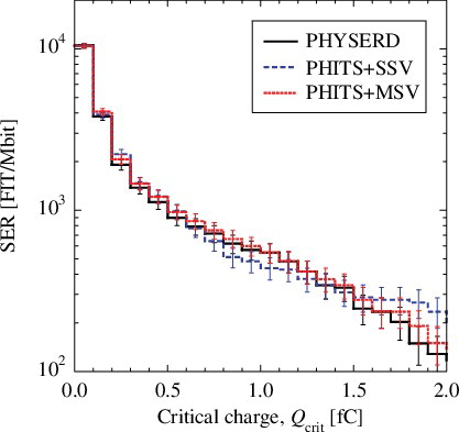
The results calculated by PHITS+MSV are compared with those obtained by PHYSERD [Citation5] and PHITS+SSV [Citation17]. Note that the size and shape of SV used in PHITS+SSV are adjusted so as to be consistent with the SERs obtained by PHYSERD as much as possible. The configuration of the SSV is also shown in . compares the SERs obtained by each simulation method. The SER obtained by PHITS+SSV is roughly consistent with that obtained by PHYSERD, although PHITS+SSV overestimates the SER for a critical charge greater than 1.5 fC. PHITS+MSV improves the estimate of the SER over the whole range of critical charge.
Figure 8. SERs as a function of critical charge calculated by PHYSERD, PHITS+SSV and PHITS+MSV.
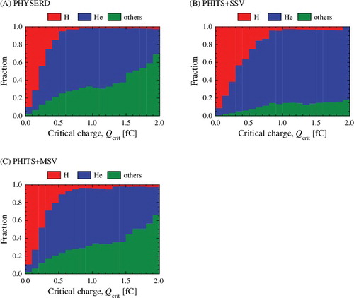
and show impacts of each incident neutron energy range and secondary ion species on the SER obtained by each simulation method, respectively. PHITS+SSV overestimates the contribution of low-energy neutrons below 10 MeV, and underestimates the contribution of high-energy neutrons above 800 MeV. For impact of secondary ion species, PHITS+SSV overestimates the contribution of H and He ions and underestimates the contribution of heavy ions. These results suggest that PHITS+SSV with the size and shape of SV adjusted to correspond to the neutron-induced SER with an energy spectrum given by JEDEC standard cannot reproduce SERs for different radiation environments (e.g., accelerator facilities with different neutron spectrum, space environment surroundings with primary cosmic-ray protons and heavy ions, and so on). In contrast, PHITS+MSV reproduces the impact of incident neutron energies and secondary ion species obtained by PHYSERD very well.
Figure 9. Impact of incident neutron energy ranges on SER obtained by (A) PHYSERD, (B) PHITS+SSV and (C) PHITS+MSV.
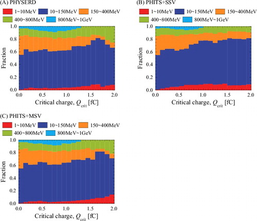
Figure 10. Impact of secondary ion species on SER obtained by (A) PHYSERD, (B) PHITS+SSV and (C) PHITS+MSV.
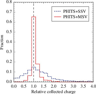
In order to validate the event reproducibility for the two SV models, the relative collected charge (i.e., the ratio of collected charge obtained by using the SV model to that obtained by using PHYSERD) was calculated for each single event. shows the event distribution of the relative collected charge for each SV model. The integral of each histogram is normalized to unity. About 90% of events are consistent within 30% of the collected charge for PHITS+MSV, whereas less than 40% of events are consistent for PHITS+SSV. This result indicates that SSV model cannot reproduce collected charge for each single event even though the SER is coincidental for that obtained by PHYSERD. The reproducibility of collected charge for each single event is improved by using the MSV model and the given conditions to consider spatial dependence of the CCE and the position where ions strike.
Figure 11. Event distribution of relative collected charges obtained by PHITS+SSV and by PHITS+MSV. Each histogram is normalized to unity.
For the conditions used in this study, we analyzed about 1000 events and it took about 40 days/CPU to obtain collected charges using HyENEXSS. The computational time required to calculate the collected charge in a single event by using the MSV model is only 0.2% of that required when using HyENEXSS. Note that PHYSERD, PHITS+SSV and PHITS+MSV require almost the same computational time for particle-transport calculations by PHITS. The computational time required to calculate the SER by PHITS+MSV, including the investigation of CCE, is approximately one-fourth of that required while using PHYSERD. Moreover, once appropriate CCEs and SVs are defined for the NMOSFET, PHITS+MSV can estimate the SERs for various conditions (e.g., different memory-cell layouts and/or radiation environments) in half the computational time required for the initial PHITS+MSV calculation.
4. Conclusion
Secondary cosmic-ray neutron-induced soft errors in a 25-nm bulk-design NMOSFET were analyzed based on the MSV model using PHITS. The condition of the MSVs was defined based on a systematic investigation of the charge collection process with HyENEXSS. The results of the soft error analysis by PHITS+MSV have been compared with those obtained by PHYSERD based on an event-by-event TCAD simulation and PHITS+SSV. The SER and the impact of incident neutron energies and secondary ion species calculated by PHITS+MSV are consistent with those obtained by PHYSERD. Through the comparison of the collected charges obtained by TCAD simulation and by SV model calculations for each single event, it has been demonstrated that the reproducibility of collected charges based on the SV model is improved by considering spatial dependence of the CCE and the position where ions strike. For the calculation conditions used in this study, the computational time required for PHITS+MSV, including the time required to investigate CCEs by HyENEXSS, is reduced by a factor of 4 when compared with that for PHYSERD. Furthermore, once the CCE is derived and appropriate SVs are defined, PHITS+MSV can estimate SERs in half the computational time compared with that required for the initial calculation. Therefore, PHITS+MSV proves to be the most suitable among the methods compared in this study to estimate SERs in the practical design of semiconductor devices which requires not only accuracy but also computation speed.
Disclosure statement
No potential conflict of interest was reported by the authors.
References
- Reed RA, Weller RA, Akkerman A, et al. Anthology of the development of radiation transport tools as applied to single event effects. IEEE Trans Nucl Sci. 2013;60:1876–1911.
- Tosaka Y, Satoh S, Oka H. An accurate and comprehensive soft error simulator NISES II. Proceedings of Simulation of Semiconductor Processes and Devices (SISPAD 2004); 2004 Sep 2–4; Munich, Germany.
- Nakamura T, Ibe E, Yahagi Y, et al. Neutron-induced soft-error in advanced memory devices. Singapore: World Scientific; 2008.
- Abe S, Watanabe Y, Shibano N, et al. Multi-scale Monte Carlo simulation of soft errors using PHITS-HyENEXSS code system. IEEE Trans Nucl Sci. 2012;59:965–970.
- Abe S, Watanabe Y. Neutron-induced soft error analysis in MOSFETs from a 65 nm to a 25 nm design rule using multi-scale Monte Carlo simulation method. Proceedings of International Reliability Physics Symposium (IRPS 2012); 2012 Apr 15–19; Anaheim, CA.
- Abe S, Ogata R, Watanabe Y. Impact of nuclear reaction models on neutron-induced soft error rate analysis. IEEE Trans Nucl Sci. 2014;61:1806–1812.
- Sato T, Niita K, Matsuda N, et al. Particle and heavy ion transport code system PHITS, version 2.52. J Nucl Sci Technol. 2013;50:913–923.
- 3-D TCAD simulator HyENEXSS [DVD]. Kanagawa, Japan: Semiconductor Leading Edge Technologies Inc., Semiconductor Technology Academic Research Center; c2002–2011. 1 DVD: 4 3/4 in. Accompanied by 24 manuals and user guides. Japanese.
- Abe S, Watanabe Y. Analysis of charge deposition and collection caused by low energy neutrons in a 25-nm bulk CMOS technology. IEEE Trans Nucl Sci. 2014;61:3519–3526..
- Kato T, Akano R, Uemura T, et al. Neutron shielding effect of stacked servers and its impact on reduction of soft error rate. IEEE Trans Nucl Sci. 2014;61:3408–3415.
- Petersen EL, Pickel JC, Smith EC, et al. Geometrical factors in SEE rate calculations. IEEE Trans Nucl Sci. 1993;40:1888–1909.
- Warren KM, Weller RA, Sierawski BD, et al. Application of RADSAFE to model the single event upset response of a 0.25 μm CMOS SRAM. IEEE Trans Nucl Sci. 2007;54:898–903.
- Sannikov AV. Single event upsets in semiconductor devices induced by highly ionising particles. Radiat Prot Dosimetry. 2004;110:399–403.
- Tosaka Y, Kanata H, Satoh S, et al. Simple method for estimating neutron-induced soft error rates based on modified BGR model. IEEE Electron Device Lett. 1999;20:89–91.
- Tang HHK, Cannon EH. SEMM-2: a modeling system for single event upset analysis. IEEE Trans Nucl Sci. 2004;51:3342–3348.
- Wrobel F, Saigne F. Monte Carlo simulation of neutrons, protons, ions and alpha particles involved in soft errors in advanced memories. Prog Nucl Sci Technol. 2011;2:582–586.
- Abe S, Watanabe Y. Validation of sensitive volume size based on a multi-scale Monte Carlo simulation in neutron-induced soft error analyses. Proceedings of the 10th International Workshop on Radiation Effects on Semiconductor Devices for Space Applications (10th RASEDA); 2012 Dec 10–12; Ibaraki, Japan.
- Boeuf F, Sellier M, Farcy A, et al. An evaluation of the CMOS technology roadmap from the point of view of variability interconnects, and power dissipation. IEEE Trans Electron Devices. 2008;55:1433–1440.
- ITRS 2009 edition, Interconnect [Internet]. International Technology Roadmap for Semiconductors; 2009. 83 p. Available from: http://www.itrs.net/reports.html
- Hanson S, Seok M, Sylvester D, et al. Nanometer device scaling in subthreshold logic and SRAM. IEEE Trans Electron Devices. 2008;55:175–185.
- Kato T, Uemura T, Mori H, et al. Impact of parasitic bipolar effect on single-event upset in p-type metal-oxide-semiconductor field effect transistor with embedded SiGe. J Appl Phys. 2013;52:04CC15.
- Measurement and reporting of alpha particle and terrestrial cosmic ray-induced soft errors in semiconductor devices [Internet]. JEDEC; 2006 Oct. 84 p. Document No.: JESD89A. Available from: http://www.jedec.org