
 ?Mathematical formulae have been encoded as MathML and are displayed in this HTML version using MathJax in order to improve their display. Uncheck the box to turn MathJax off. This feature requires Javascript. Click on a formula to zoom.
Abstract
Monolayers of free base phthalocyanine (H2Pc) are grown on monolayer and few-layer exfoliated flakes of hexagonal boron nitride (hBN) which are subsequently integrated into a van der Waals tunnel diode. This heterostructure consists of two thin hBN flakes between which the H2Pc monolayer is sandwiched and also incorporates upper and lower few-layer graphene contacts. When a voltage is applied between the contacts, a tunnel current flows and the embedded molecules can be excited resulting in the emission of photons with wavelengths which are close to the peaks observed in photoluminescence. We also observe electroluminescence at voltages where the energy gained by a tunnelling electron is lower than the energy of the emitted photon implying a multi-electron excitation pathway which we attribute to the formation of an intermediate triplet state. Our results provide insights into the differences in excitation and relaxation of molecules in supramolecular monolayers and bulk crystals and we discuss how the alignment of the energy levels of the molecules and contact layers determine the emission process.
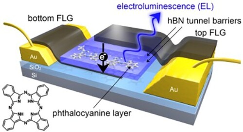
GRAPHICAL ABSTRACT
The integration of monolayers of planar organic molecules with van der Waals heterostructures enables the formation of molecular/2D hybrid tunnel diodes and related structures with novel optoelectronic properties [Citation1–5]. Such vertically stratified structures are of great interest as they further enrich the set of parameters addressable in the exploration of van der Waals heterostructures through control over the molecular structure and their arrangement. Applications which have already been identified include the modification of molecular arrangement to favour stronger light–matter interactions in molecular aggregates [Citation4,Citation6–9], intersystem crossing in molecular systems [Citation5], environmental protection [Citation10] and modifying the vibrational properties of molecules sandwiched at interfaces [Citation11]. The formation of such heterostructures provides myriad directions for research into the detection, harvesting and emission of light as well as opportunities to manipulate and control the optoelectronic properties of nanostructures [Citation12].
In this work, we fabricate light-emitting devices based upon van der Waals heterostructures [Citation13–16] in which monolayers of self-assembled free base phthalocyanine molecules (H2Pc) are incorporated into a hexagonal boron nitride (hBN) tunnel diode [Citation17,Citation18]. In the molecular hybrid version of these structures, we have previously shown that the trapped molecules may be excited into both spin-singlet and -triplet states which can subsequently relax through the emission of photons, thus forming an electroluminescent device [Citation5,Citation19]. The close proximity (< 1 nm) between the organic emissive layer and the contact layers in these devices is analogous to scanning tunnelling microscopy luminescence (STML) experiments in which electroluminescence from organic molecules, separated from a metallic substrate by ultra-thin alkali halide layers, is induced by tunnelling between the STM tip and substrate [Citation20–26]. This architecture is distinct from that of conventional organic electroluminescent devices, where carriers are typically injected from remote contacts with an engineered work function and form excitons which diffuse to an emissive centre and recombine [Citation27,Citation28]. In our previous studies we have investigated electroluminescence from hybrid devices with trapped perylene tetracarboxylic di-imide (PTCDI) molecules [Citation5] and, also, monolayers of polythiophene adsorbed with their conjugated backbone aligned parallel to the hBN tunnel barriers [Citation19,Citation29]. In our current paper we study a device incorporating a H2Pc monolayer. This molecule differs significantly from PTCDI since the frontier orbitals, particularly the highest occupied molecular orbital (HOMO), lie at much higher energies. We argue that this difference in energy levels leads to an alternative relaxation mechanism for the triplet state of H2Pc. Our work shows the importance of the alignment of energy levels in the control of the lifetime of excited states of trapped molecules.
We use polymer stamp-assisted van der Waals assembly [Citation30–33] to fabricate our devices. In this approach, flakes of few-layer graphene (FLG) and hBN are sequentially picked up to form a van der Waals stack in which a tunnel barrier is positioned between two FLG layers which can be independently contacted. To fabricate a device we first use a polymer stamp to pick up a large (lateral dimensions 10 s of μm) thick (10 s of nm) hBN flake, which is ultimately used to cap the device. This hBN flake is then used to pick up a FLG flake which serves as the top contact of the completed device, followed by an hBN flake with thickness of, typically, 1–3 monolayers which forms the upper tunnel barrier. This van der Waals stack is then used to pick-up a second hBN tunnel barrier, also with a thickness of 1–3 monolayers, on which a H2Pc monolayer has been pre-deposited by sublimation as described previously [Citation34]. This part-formed tunnelling device is then released from the stamp onto a second FLG flake which forms the lower contact and has been pre-deposited on a supporting substrate (Si/SiO2); the release site is chosen so that the upper and lower graphene layers make independent contact with two pre-formed metallic (Cr/Au) electrodes which can be connected to external wiring. Further details are provided in Supplementary Information (SI).
The completed device consists of a monolayer of H2Pc sandwiched between few layer hBN and overlaid FLG contacts, as depicted in Figure (a) (the upper thick hBN layer, and a supporting thick hBN flake which provides a supporting substrate for the lower graphene are omitted for clarity; neither plays an active role in the device operation). The FLG provides transparent top- and bottom-electrodes allowing carrier transport through the H2Pc monolayer under an applied bias.
Figure 1. FLG/hBN/H2Pc/hBN/FLG heterostructures. a Schematic of device in which a monolayer of H2Pc is encapsulated between two hBN tunnel barriers and charge can be transported between upper and lower FLG contacts under the application of an applied bias; lower left – schematic of the molecular structure of H2Pc. b AFM image of a monolayer coverage of H2Pc on hBN. Inset, high resolution image with schematic overlay. c Optical image of a device showing gold contacts and the van der Waals heterostructure. The dashed line indicates the active area of the device where the upper and lower FLG layers overlap. Inset top: SEM image of the highlighted area in false colour showing the FLG (grey) and hBN layers (blue). Inset bottom: scanning electroluminescence image taken at a +2.2 V bias and 1 s integration time confirming that light is emitted from the active area of the device. d current–voltage (black) and differential current-voltage (blue) characteristics. Inset: current-voltage on a logarithmic scale. e Electroluminescence spectrum. Inset, black: experimental PL spectrum, grey: fit using three Lorentzian curves with peak positions 704, 720 and 741 nm. Scale bars b 15 nm, b inset 2 nm, c main image and insets 10 μm.
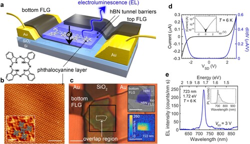
Images acquired using high-resolution atomic force microscopy (AFM) of a sublimed H2Pc monolayer on an hBN flake are shown in Figure (b) and reveal the expected [Citation34] near-square regular array of flat-lying molecules (the deposition and characterisation of H2Pc and preparation of the hBN surface prior to incorporation in the device follow our previous work [Citation34] and are discussed in SI; the structure of the molecule is shown in Figure (a)). An optical image of a completed device is shown in Figure (c); the active area of the device is marked and corresponds to the region where the upper and lower FLG layers overlap. The different layers are resolved more clearly in the image acquired using scanning electron microscopy in Figure (c) inset; here the hBN and FLG are highlighted. Overall, this device corresponds to a heterostructure with the sequence hBN/FLG/hBN/H2Pc/hBN/FLG/hBN.
The bottom and top FLG are contacted to Cr/Au electrodes which are shown, respectively, on the left and the right side of the optical image (Figure (c)). The current–voltage characteristics of the device were measured in an optical cryostat at a temperature T = 6 ± 2 K, and are highly non-linear as expected for a tunnelling device (see Figure (d); note the near-exponential rise in current revealed in the inset to Figure (d)). For this device the current–voltage dependence is highly symmetric with respect to polarity which indicates that the upper and lower barriers have the same thickness. The effective area of the device is estimated to be 26 ± 2 μm2.
The photoluminescence from the active region of our device has been measured (see inset in Figure (e); excitation laser 405 nm focussed using a 50x objective lens to a spot with a diameter ∼ 2 μm – see SI for further details) and may be decomposed into three peaks at wavelengths 704 ± 1, 720 ± 1 and 741 ± 2 nm (corresponding respectively to 1.76, 1.72 and 1.67 eV). The peaks at 704 and 741 nm are close to the values recently determined for, respectively, the 0–0 direct (706 ± 2 nm) and 0–1 vibronic (742 ± 2 nm) transitions in the photoluminescence spectrum of an H2Pc monolayer [Citation34] adsorbed on uncapped hBN. The peak at 720 nm is not observed in the spectrum for uncapped H2Pc, and we suggest that this feature arises from molecules which are trapped between the hBN layers. The red-shift of the 0–0 peak of the encapsulated molecules by ∼ 20 nm, compared to H2Pc on uncapped hBN, represents a shift in photon energy ∼ 40 meV.
It is interesting to compare the energies/wavelengths of the 0–0 direct transition of H2Pc in the gas phase [Citation35] (1.876 eV/661 nm), adsorbed as a flat-lying monolayer on hBN [Citation34] (1.76 eV/706 nm) and as a flat-lying monolayer sandwiched between two hBN layers (1.72 eV/720 nm) as in the current work. We have shown previously that [Citation4] a red-shift (relative to the gas phase) is expected when a planar organic molecule is absorbed on an insulator. This is due to the dielectric effect of the substrate which results in a non-resonant red-shift due to the screening of the electrostatic interactions within the adsorbed molecule giving rise to changes to the frontier energy levels and relevant electron–hole interactions. The transition energies for molecules in the gas phase, adsorbed on uncapped hBN and trapped between two hBN layers can be calculated using time-dependent density function theory (TDDFT) as described in SI. The predicted transition energies are 1.84, 1.75 and 1.68 eV for H2Pc in, respectively, the gas-phase, adsorbed on uncapped hBN and trapped between two hBN layers. These values are in good agreement with experimental observations and reproduce the trend of progressively larger red-shift in the different hBN environments. In our previous work we have also noted [Citation4,Citation34] that additional resonant shifts occur due to the coupling of the transition dipole moment with image charges in the dielectric substrate, and also through coupling with the transition dipoles of neighbouring molecules. However, for H2Pc on hBN these effects lead to red-shifts which are much smaller than the non-resonant effects [Citation34] and so are not considered further here.
The devices emit light when a current flows. Figure (e) shows the electroluminescence spectrum which reveals a dominant peak at 723 ± 1 nm with a width of 15 nm (this measurement is derived from light emitted from the whole device area). This peak is attributed to electron–hole radiative recombination by electrically excited H2Pc molecules. This is further confirmed by a map of the electroluminescence showing the spatial variation of the peak intensity – see Figure (c) inset – which confirms that the active region of the device, where the FLG/hBN/H2Pc/hBN/FLG overlap, is the source of the photon emission. The electroluminescence peak emission is close to the position of the peak in PL at 720 nm, which is attributed above to encapsulated molecules. Note that only the encapsulated molecules would be expected to couple strongly to the FLG contact layers, so the additional peaks in PL at 704 and 742 nm would be expected to appear only in PL and not EL, in agreement with our observations. It is likely that the PL peaks at 704 and 741 nm are either due to emission from molecules from surrounding regions which are excited by scattered incident light, or molecules which are not efficiently trapped between the hBN layers due to inhomogeneities in the fabricated device, so that their emission is characteristic of uncapped H2Pc. We also observe a small peak in the EL spectrum at 689 ± 2 nm which we attribute to an anti-Kasha (1–0) vibronic transition (a similar peak has recently been reported in STML studies of napthalocyanine [Citation36]). We thus attribute the EL emission to radiative electron–hole recombination by electrically excited H2Pc molecules encapsulated with hBN.
The spectra recorded at different voltages are presented in the form of a colour map in Figure which shows that the position and line width of the EL peak is voltage-independent. The integrated EL intensity for this device is also shown in Figure . The EL spectra do not show a strong polarity dependence (in our measurements the voltage is applied to the top contact); additional results on voltage dependence are included in SI (Figures S4 and S5).
Figure 2. Electroluminescence in FLG/hBN/H2Pc/hBN/FLG heterostructures measured at room temperature. Colour map of the EL spectra as a function of applied bias. White circles, right axis: integrated intensity of EL over the wavelength range 700–750 nm.
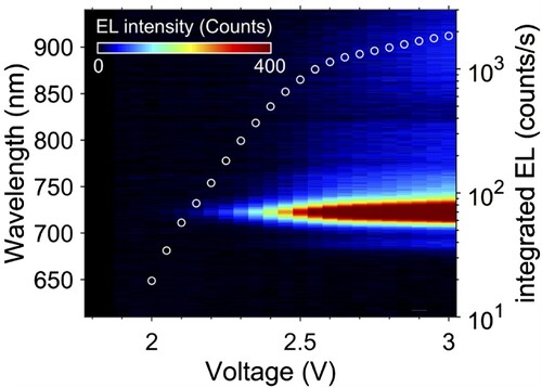
Figure 3. Electroluminescence spectra acquired at T = 6 ± 2 K from a FLG/hBN/H2Pc/hBN/FLG heterostructure device for a series of bias voltages ranging from −1.5 to −1.9 V. The bias voltage and acquisition time for each spectrum is annotated in the corresponding colour. The spectra acquired at −1.6 and −1.7 V exhibit photon up-conversion.
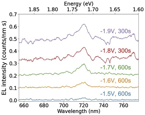
We have also investigated EL at voltages close to the onset for photon emission as shown in Figure . Measurements at each voltage were performed with acquisition times ranging from 100s to 600 s; the longer acquisition times were required for the detection of weaker EL emission at smaller (absolute) bias voltages. An EL emission peak located at 720 ± 4 nm can be observed in Figure for each bias voltage value in the range −1.6 V to −1.9 V. This peak position is consistent with emission from the encapsulated H2Pc monolayer, as discussed above. Interestingly, EL is detected at bias voltages of −1.6 V and −1.7 V (our detection of EL peaks at lower voltage is limited by noise in our CCD detection electronics; a very weak peak at −1.5 V cannot be ruled out). In this voltage range the energy of the emitted photons, , the energy gained by the tunnelling electrons due to the bias voltage between the contacts. This is an example of photon up-conversion and implies that the excitation of the molecule into the singlet state involves a multi-electron process. Up-conversion has previously been reported for similar devices containing an encapsulated monolayer of PTCDI molecules [Citation5] and also in STML studies of H2Pc [Citation24].
In similar devices which incorporate a PTCDI monolayer, it has been shown that the up-conversion process is mediated by an intermediate triplet state; this hypothesis was based on the fact that the lifetime of any intermediate state should be longer than the typical time between successive electron tunnelling events (which can be deduced from the current density and the molecular dimensions). The role of triplet intermediates was confirmed by the presence of an additional peak in the PTCDI EL spectrum due to triplet emission. In the proposed mechanism the PTCDI was first excited to a triplet state, and then, in a second inelastic event, excited from the triplet to the excited singlet state. In the H2Pc analogue device considered here we observe a similar up-conversion and propose that a similar mechanism is responsible. We note that photon emission from H2Pc is observed at a measured current density of 6.5 µA µm−2 (at VSD = −1.6 V). Taking the area per molecule to be 2.25 nm2, we estimate a lower bound for the average time interval between electrons tunnelling through an effective molecular area to be 11 ± 2 ns. The lifetime of the H2Pc triplet state is much longer, of the order 130 µs [Citation37], confirming that this state can participate as an intermediary in a multi-electron inelastic scattering pathway (note that the lifetime of other excited states, such as vibronic states are expected to be much shorter). In the proposed mechanism, a 2-step inelastic tunnelling process leads to up-conversion. The first inelastic scattering event excites the molecule into the triplet state (T1). This state is sufficiently long-lived that during the triplet lifetime further inelastic tunnelling events can occur, promoting the excited electron from the T1 state into the first excited singlet state (S1), which rapidly relaxes via the emission of a photon.
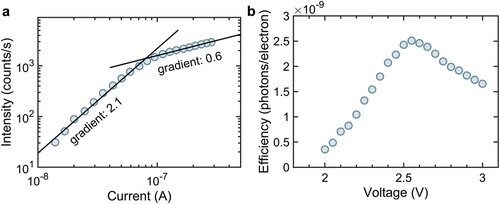
As expected for a multi-electron process we observe a super-linear dependence of intensity on current, I, for low voltages (intensity ∝ I2.1 see Figure (a)) similar to that reported in recent STML studies [Citation24] of H2Pc which were also attributed to triplet-mediated up-conversion. We also observe a significant change in the dependence of intensity on current at a voltage of ∼2.54 V. This is apparent in Figure (a) and, consequently, corresponds to a reduction in the EL efficiency (photons emitted per tunnelling electron) as shown in Figure (b). Within the model proposed above this implies the appearance of a voltage-dependent mechanism for the relaxation of intermediate triplet states. Interestingly, this behaviour is not observed in the analogue PTCDI device which was reported previously [Citation5] for which the efficiency increases monotonically over the complete voltage range under investigation. It is possible that this difference arises from the relative position of the energy levels of the two molecules. PTCDI is an n-type organic semiconductor, whereas H2Pc is p-type, meaning that the HOMO of H2Pc lies at a much higher energy compared to PTCDI.
Figure 4. a Dependence of EL intensity on current; b Dependence of efficiency on applied voltage. Data are acquired at room temperature.
Energy level diagrams of the H2Pc and PTCDI devices under 0 and 1.6 V bias are shown in Figure (a–c). These energy level diagrams illustrate the relative energies of the HOMO, LUMO, S1, and T1 states of H2Pc and PTCDI compared to the Fermi levels of the FLG electrodes. The energies of the S1 and T1 states were obtained, respectively, from experimental values and the literature [Citation37], and the HOMO/LUMO values determined from theoretical calculations (see SI). In the absence of an applied voltage (Figure (a)), both the S1 and T1 energy levels of H2Pc lie below the Fermi level of the FLG electrodes and no current flows through the device. When the device is under bias, however, the relative positions of the energy levels of the FLG and H2Pc shift due to the applied voltage. This is demonstrated schematically in Figure (b), while Figure (c) shows an equivalent diagram for a PTCDI device. The application of an applied voltage leads to changes in the carrier concentrations in each electrode and, consequently, a shift in the Fermi level of the top and bottom () electrodes and, in addition, a relative shift of the Dirac point such that the total energy difference between the FLG Fermi levels is equal to eVSD (see SI for details of these calculations). The molecular energy levels are also shifted, and, assuming that the hBN barriers have the same thickness, the energy levels are shifted by half the bias voltage (
) relative to their position under zero bias.
Figure 5. Energy level diagrams for a H2Pc tunnelling device under zero bias (a), 1.6V bias (b), and a PTCDI tunnelling device under 1.6V bias (c). Inelastic electron scattering (IES) events are labelled. (a) Under zero bias both the H2Pc singlet, S1, and triplet, T1, states lie below the Fermi energy of the bottom graphene electrode, . (b) At 1.6V bias, T1 lies 100 meV above
. Up-converted electroluminescence from S1 is observed at 1.6V bias. (c) The lower-lying energy levels of PTCDI mean that under 1.6V bias, both S1 and T1 lie below
and emission is observed from both states.
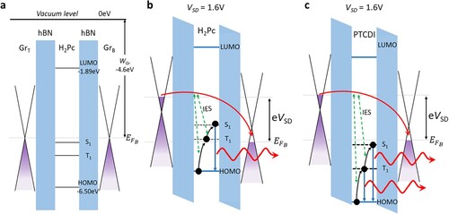
From a comparison of Figure (a,b), it can be seen that the relative alignment of the H2Pc T1 level and changes significantly when a 1.6 V bias is applied. In Figure (a), T1 lies 0.7 eV below
, whereas in Figure (b), the shifting of energy levels results in T1 lying 0.1 eV above
. In contrast, since the frontier energy levels of PTCDI are much lower-lying than the corresponding states in H2Pc, the PTCDI T1 and S1 energy levels lie below
(Figure (c)) under a bias of 1.6 V. It is possible that an additional non-radiative pathway for triplet relaxation could occur for voltages at which the triplet energy is raised above the Fermi energy of the adjacent electrode, for example due to ionisation, which might account for the reduction in efficiency observed at high voltage (Figure (b)). From our simple model presented in Figure we predict that the triplet state is in alignment with the Fermi level for voltages of 1.4 V (H2Pc) and 3.8 V (PTCDI). While this is consistent with presence (absence) of reduction in efficiency for H2Pc (PTCDI), the measured voltage position of the peak efficiency of H2Pc is significantly higher than the calculated threshold for triplet/Fermi level alignment. This difference may be due to uncertainties in the values used for the HOMO and triplet energies, but may also be affected by additional energy barriers due to electrostatic effects, as well as dynamic factors involving tunnelling rates which are also expected to be voltage-dependent. Implicit in our argument is that, since up-converted emission from the singlet state is observed, the triplet relaxation time of this additional pathway is longer than the time between successive electron traversal time (11 ns) but shorter than the lifetime of the triplet state. This implies a prospective relaxation time, tn-r, for this non-radiative pathway in the range, 10 ns
130 μs. Notably, this relaxation time is much longer than the lifetime of the singlet state (∼250 ps) [Citation38] and so would not be expected to suppress singlet emission. We also note that the efficiency of our H2Pc devices, typically 10−9–10−10 photons per electron, is lower than that of analogue PTCDI devices, (10−6–10−8 photons per electron [Citation5]).
Our results show that electroluminescence from molecular/2D van der Waals heterostructures can occur for organic molecules with widely varying frontier orbital energies. This suggests a common mechanism for excitation and relaxation of the molecules and the observation of photon up-conversion which we observe for both H2Pc and PTCDI is suggestive of a long-lifetime intermediate state which, as we argue above, we attribute to a triplet. Interestingly, for both the PTCDI and the H2Pc devices discussed here, a peak in the EL spectrum which can be assigned to an anti-Kasha (1–0) vibronic transition [Citation36] is observed. Although the peak has low intensity, its presence suggests that molecules may also be vibrationally excited due to inelastic energy transfer from the tunnelling electrons so that there is a non-equilibrium occupation of vibrational levels; this peak is not observed in the PL spectra of either molecule.
Despite the similarities between the properties of our H2Pc and previously published PTCDI devices, the absence of emission from the triplet state in the current study represents a significant difference. In our previous work [Citation5] we observed a clear peak in the EL spectrum which was assigned to triplet emission. It is possible that the additional relaxation pathways for triplets (see above) may account for the absence of a triplet emission peak in the current work, although we cannot rule out other explanations such as an intrinsically lower rate for triplet emission from H2Pc molecules in the device structure, or that the signal is beyond the detection limits of our experimental arrangement (note the lower efficiency even for singlet emission discussed above).
Moreover, it has recently been suggested that the assignment of emission from a triplet in a related STML study [Citation39] is actually due to trion emission from a charged molecule. Although not directly relevant to the results discussed here, it is interesting to consider whether trions might play a role in the EL of molecular/van der Waals tunnel devices. Trion emission occurs when singly-charged molecular anions are excited into a doublet state and subsequently relax through the emission of a photon; this transition conserves spin and is optically-allowed. We would expect that both trion emission, and the presence of long-lived charged molecules in our devices would be detected in changes in the voltage-dependent PL of our device structures. In fact, PL measurements reveal a complete absence of any voltage dependence. These data were previously reported for the PTCDI variation of the device (Ref Citation5 SI Figure S6) and similar measurements for the current study on H2Pc are shown in SI (Figure S6); for both molecules the PL peak positions are close to those previously reported for the same molecules on thick hBN flakes [Citation4,Citation34] and confirm that the molecules remain neutral over the measured voltage range. These results show charged molecules cannot account for the long-lived intermediary excited states which are necessary for up-conversion and which have been previously attributed to the presence of triplets [Citation5,Citation24]. However, it is not possible to rule out (or in) a possible pathway in which a long-lived triplet acquires a charge via electron capture followed by rapid relaxation via trion emission. To determine whether this process might be relevant would require the identification of the spectral position for trion emission for PTCDI which would, in turn, require a means of forming an ensemble of charged molecules for investigation using PL. Interestingly this may be possible using an asymmetric variation of our device in which the upper and lower barrier thicknesses are significantly different and we plan to undertake such studies in the near future.
Currently there is no detailed theoretical framework to underpin the phenomenological explanations reported here and our work motivates further studies of the mechanisms of energy transfer from tunnelling electrons to organic molecules, including transitions to the triplet state which are optically-forbidden. While there remain some uncertainties in the detailed explanations of the optoelectronic properties of our devices, we stress that the current work provides insights into the possible role of energy level alignment on the generation of stable intermediary states of relevance to the fundamental study of long-lived molecular excited states with potential applications in quantum spin-based technologies and, through photon up-conversion, low-voltage light emitting devices.
Supplemental Material
Download MS Word (1.8 MB)Acknowledgements
We are grateful to the Engineering and Physical Sciences Research Council for support through grant EP/N033906/1. A.S.N. is grateful to the Ministry of Science and Higher Education (Agreement No. 121031700313-8). We thank Bjarke Sørensen Jessen for helpful discussions. K.W. and T.T. acknowledge support from the JSPS KAKENHI (Grant Numbers 19H05790, 20H00354 and 21H05233). P.H.B thanks the Leverhulme Trust for the award of a Research Fellowship [RF-2019-460]. This work evolved from the study of the influence of absorption on the transition energies of organic molecules which was initiated in collaboration with Professor Nick Besley to whom this paper is dedicated.
Data availability statement
The authors declare that the data supporting the findings of this study are available within the article and its Supplementary Information files, or from the corresponding author on reasonable request.
Disclosure statement
No potential conflict of interest was reported by the author(s).
Additional information
Funding
References
- S.H. Amsterdam, T.J. Marks and M.C. Hersam, J. Phys. Chem. Lett. 12, 4543 (2021). doi:10.1021/acs.jpclett.1c00799
- J.H. Park, A. Sanne, Y. Guo, M. Amani, K. Zhang, H.C.P. Movva, J.A. Robinson, A. Javey, J. Robertson, S.K. Banerjee and A.C. Kummel, Sci. Adv. 3, e1701661 (2017). doi:10.1126/sciadv.1701661
- Y.L. Huang, Y.J. Zheng, Z. Song, D. Chi, A.T.S. Wee and S.Y. Quek, Chem. Soc. Rev. 47, 3241 (2018). doi:10.1039/C8CS00159F
- J. Kerfoot, V.V. Korolkov, A.S. Nizovtsev, R. Jones,T. Taniguchi, K. Watanabe, I. Lesanovsky, B. Olmos,N.A. Besley, E. Besley and P.H. Beton, J. Chem. Phys. 149, 054701 (2018). doi:10.1063/1.5041418
- S.A. Svatek, J. Kerfoot, A. Summerfield, A.S. Nizovtsev, V.V.V. Korolkov, T. Taniguchi, K. Watanabe, E. Antolín, E. Besley and P.H. Beton, Nano Lett. 20, 278 (2020). doi:10.1021/acs.nanolett.9b03787
- A.S. Davydov, Sov. Phys. Uspekhi. 82, 393–448 (1964). doi:10.3367/ufnr.0082.196403a.0393.
- F.C. Spano and C. Silva, Annu. Rev. Phys. Chem. 65, 477 (2014). doi:10.1146/annurev-physchem-040513-103639
- A. Eisfeld, C. Marquardt, A. Paulheim and M. Sokolowski, Phys. Rev. Lett. 119, 097402 (2017). doi:10.1103/PhysRevLett.119.097402
- H. Zhao, Y. Zhao, Y. Song, M. Zhou, W. Lv, L. Tao, Y. Feng, B. Song, Y. Ma, J. Zhang, J. Xiao, Y. Wang, D.-H. Lien, M. Amani, H. Kim, X. Chen, Z. Wu, Z. Ni, P. Wang, Y. Shi, H. Ma, X. Zhang, J.-B. Xu, A. Troisi, A. Javey and X. Wang, Nat. Commun. 10, 5589 (2019). doi:10.1038/s41467-019-13581-9
- S. Koo, I. Park, K. Watanabe, T. Taniguchi, J.H. Shim and S. Ryu, Nano Lett. 21, 6600 (2021). doi:10.1021/acs.nanolett.1c02009
- K.S. Vasu, E. Prestat, J. Abraham, J. Dix, R.J. Kashtiban, J. Beheshtian, J. Sloan, P. Carbone, M. Neek-Amal, S.J. Haigh, A.K. Geim and R.R. Nair, Nat. Commun. 7, 12168 (2016). doi:10.1038/ncomms12168
- Y. Zhao, V. Wang and A. Javey, Matter. 3, 1832 (2020). doi:10.1016/j.matt.2020.09.009
- F. Withers, O. Del Pozo-Zamudio, A. Mishchenko, A.P. Rooney, A. Gholinia, K. Watanabe, T. Taniguchi, S.J. Haigh, A.K. Geim, A.I. Tartakovskii and K.S. Novoselov, Nat. Mater. 14, 301 (2015). doi:10.1038/nmat4205
- C. Palacios-Berraquero, M. Barbone, D.M. Kara, X. Chen, I. Goykhman, D. Yoon, A.K. Ott, J. Beitner, K. Watanabe, T. Taniguchi, A.C. Ferrari and M. Atatüre, Nat. Commun. 7, 12978 (2016). doi:10.1038/ncomms12978
- D. Kwak, M. Paur, K. Watanabe, T. Taniguchi and T. Mueller, Adv. Mater. Technol. 7, 2100915 (2022). doi:10.1002/admt.202100915
- M. Paur, A.J. Molina-Mendoza, R. Bratschitsch, K. Watanabe, T. Taniguchi and T. Mueller, Nat. Commun. 10, 1709 (2019). doi:10.1038/s41467-019-09781-y
- L. Britnell, R.V. Gorbachev, R. Jalil, B.D. Belle, F. Schedin, A. Mishchenko, T. Georgiou, M.I. Katsnelson, L. Eaves, S.V. Morozov, N.M.R. Peres, J. Leist, A.K. Geim, K.S. Novoselov and L.A. Ponomarenko, Science. 335, 947 (2012). doi:10.1126/science.1218461
- A. Mishchenko, J.S. Tu, Y. Cao, R.V. Gorbachev,J.R. Wallbank, M.T. Greenaway, V.E. Morozov, S.V. Morozov, M.J. Zhu, S.L. Wong, F. Withers, C.R. Woods, Y.-J. Kim, K. Watanabe, T. Taniguchi, E.E. Vdovin, O. Makarovsky, T.M. Fromhold, V.I. Fal’ko, A.K. Geim, L. Eaves and K.S. Novoselov, Nat. Nanotechnol. 9, 808 (2014). doi:10.1038/nnano.2014.187
- J. Kerfoot, S.A. Svatek, V.V. Korolkov, T. Taniguchi, K. Watanabe, E. Antolin and P.H. Beton, ACS Nano. 14, 13886 (2020). doi:10.1021/acsnano.0c06280
- Y. Zhang, Y. Luo, Y. Zhang, Y.-J. Yu, Y.-M. Kuang, L. Zhang, Q.-S. Meng, Y. Luo, J.-L. Yang, Z.-C. Dong and J.G. Hou, Nature. 531, 623 (2016). doi:10.1038/nature17428
- H. Imada, K. Miwa, M. Imai-Imada, S. Kawahara, K. Kimura and Y. Kim, Nature. 538, 364 (2016). doi:10.1038/nature19765
- B. Doppagne, T. Neuman, R. Soria-Martinez, L.E.P. López, H. Bulou, M. Romeo, S. Berciaud, F. Scheurer, J. Aizpurua and G. Schull, Nat. Nanotechnol. 15, 207 (2020). doi:10.1038/s41565-019-0620-x
- B. Doppagne, M.C. Chong, H. Bulou, A. Boeglin, F. Scheurer and G. Schull, Science. 361, 251 (2018). doi:10.1126/science.aat1603
- G. Chen, Y. Luo, H. Gao, J. Jiang, Y. Yu, L. Zhang, Y. Zhang, X. Li, Z. Zhang and Z. Dong, Phys. Rev. Lett. 122, 177401 (2019). doi:10.1103/PhysRevLett.122.177401
- K. Kuhnke, C. Große, P. Merino and K. Kern, Chem. Rev. 117, 5174 (2017). doi:10.1021/acs.chemrev.6b00645
- P. Merino, C. Große, A. Rosławska, K. Kuhnke and K. Kern, Nat. Commun. 6, 8461 (2015). doi:10.1038/ncomms9461
- M. Nothaft, S. Höhla, F. Jelezko, N. Frühauf, J. Pflaum and J. Wrachtrup, Nat. Commun. 3, 628 (2012). doi:10.1038/ncomms1637
- S.-J. Zou, Y. Shen, F.-M. Xie, J.-D. Chen, Y.-Q. Li and J.-X. Tang, Mater. Chem. Front. 4, 788 (2020). doi:10.1039/C9QM00716D
- V.V. Korolkov, A. Summerfield, A. Murphy, D.B. Amabilino, K. Watanabe, T. Taniguchi and P.H. Beton, Nat. Commun. 10, 1537 (2019). doi:10.1038/s41467-019-09571-6
- F. Pizzocchero, L. Gammelgaard, B.S. Jessen, J.M. Caridad, L. Wang, J. Hone, P. Bøggild and T.J. Booth, Nat. Commun. 7, 11894 (2016). doi:10.1038/ncomms11894
- L. Wang, I. Meric, P.Y. Huang, Q. Gao, Y. Gao, H. Tran, T. Taniguchi, K. Watanabe, L.M. Campos, D.A. Muller, J. Guo, P. Kim, J. Hone, K.L. Shepard and C.R. Dean, Science. 342, 614 (2013). doi:10.1126/science.1244358
- A.V. Kretinin, Y. Cao, J.S. Tu, G.L. Yu, R. Jalil,K.S. Novoselov, S.J. Haigh, A. Gholinia, A. Mishchenko, M. Lozada, T. Georgiou, C.R. Woods, F. Withers, P. Blake, G. Eda, A. Wirsig, C. Hucho, K. Watanabe, T. Taniguchi, A.K. Geim and R.V. Gorbachev, Nano Lett. 14, 3270 (2014). doi:10.1021/nl5006542
- A. Castellanos-Gomez, M. Buscema, R. Molenaar, V. Singh, L. Janssen, H.S.J. van der Zant and G.A. Steele, 2D Mater. 1, 011002 (2014). doi:10.1088/2053-1583/1/1/011002
- M. Alkhamisi, V.V. Korolkov, A.S. Nizovtsev, J. Kerfoot, T. Taniguchi, K. Watanabe, N.A. Besley, E. Besley and P.H. Beton, Chem. Commun. 54, 12021 (2018). doi:10.1039/C8CC06304D
- C. Murray, N. Dozova, J.G. McCaffrey, N. Shafizadeh, W. Chin, M. Broquier and C. Crépin, Phys. Chem. Chem. Phys. 13, 17543 (2011). doi:10.1039/c1cp22039j
- H. Imada, M. Imai-Imada, X. Ouyang, A. Muranaka and Y. Kim, J. Chem. Phys. 157 (2022). doi:10.1063/5.0102087
- J. McVie, R.S. Sinclair and T.G. Truscott, J. Chem. Soc. Faraday Trans. 2. 74, 1870 (1978). doi:10.1039/f29787401870
- B.W. Caplins, T.K. Mullenbach, R.J. Holmes andD.A. Blank, J. Phys. Chem. C. 119, 27340 (2015). doi:10.1021/acs.jpcc.5b09817
- K. Kimura, K. Miwa, H. Imada, M. Imai-Imada,S. Kawahara, J. Takeya, M. Kawai, M. Galperin and Y. Kim, Nature. 570, 210 (2019). doi:10.1038/s41586-019-1284-2