
 ?Mathematical formulae have been encoded as MathML and are displayed in this HTML version using MathJax in order to improve their display. Uncheck the box to turn MathJax off. This feature requires Javascript. Click on a formula to zoom.
ABSTRACT
Electrochemical surface-enhanced Raman spectroscopy (E-SERS) is a powerful technique for the detection of trace levels of analytes in solution. It has wide ranging applications with a particular focus on biomarker detection. To perform E-SERS, nanostructured plasmonic metal electrodes are needed. Currently, a variety of fabrication methods are employed. This review defines the requirements for E-SERS electrodes and then describes and evaluates the current fabrication methods. The limitations of these techniques are discussed with the balance between ease of manufacture and magnitude of enhancement being identified as the key issue. Finally, suggestions for future areas of research are presented.
Introduction
For the vast majority of diseases, early detection and diagnosis can lead to better treatment and improved quality of life [Citation1,Citation2]. Many of these illnesses can be identified by detecting specific molecules found in bodily fluids such as blood, urine or saliva, called biomarkers [Citation3]. Biomarkers can include proteins, DNAs, RNAs, lipids and metabolites [Citation4–6]. Therefore, there is a need for sensitive, selective chemical sensors which can detect biomarkers quickly and cheaply.
Effective sensors do already exist for certain conditions, such as the HIV antibody test and the preeclampsia urine test, but most are not sensitive or specific enough. Analytical methods, such as liquid chromatography-mass spectrometry and high-performance liquid chromatography, can achieve low detection limits but are time consuming and require expensive lab-based equipment [Citation7].
In recent years, research has focussed on developing rapid, cost-effective point-of-care sensors. Some of the key areas of focus have been electrochemical (EC) biosensors [Citation8–10], lateral flow assays [Citation2,Citation11], fluorescence-based optical biosensors [Citation12–14] and gravimetric biosensors [Citation15,Citation16]. However, achieving the required levels of sensitivity and specificity simultaneously is often very difficult [Citation17]. Surface-enhanced Raman spectroscopy (SERS) has been heralded as a technique which could overcome these limitations [Citation18]. Despite this, it is still yet to achieve clinical use. Electrochemical SERS (E-SERS) is a type of SERS which combines electrochemistry and conventional SERS, which has the potential to reliably detect very low (<µM) concentrations of a biomarker in a complex biological liquid.
Principles of SERS
Raman spectroscopy is an analytical technique typically used to determine the vibrational and rotational states of a molecular system [Citation19]. It provides a ‘structural fingerprint’ of a molecule by detecting the small fraction of light (approximately 1 in 107 photons) which is inelastically scattered [Citation20]. Raman spectroscopy can be used to study a wide range of materials, but it is not sensitive enough to detect biomarkers in bodily fluids due to the weak Raman scattering.
SERS is a type of Raman spectroscopy in which the signal is enhanced (by factors of up to 108) due to the adsorption of the target molecule onto a nanostructured metal surface [Citation18]. SERS was discovered in 1974 by Fleischmann et al. when an unexpectedly large Raman signal was observed while studying pyridine on an electrochemically roughened silver electrode [Citation21]. This was the start of a lengthy debate into the reason for the SERS enhancement which has only recently reached a good agreement among researchers. It is now understood to be a combination of an electromagnetic (EM) and a chemical enhancement [Citation18,Citation22,Citation23].
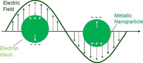
The EM enhancement is the result of an increase in the local EM field at the surface of the metal caused by local surface plasmon resonance (LSPR) [Citation18,Citation23,Citation24]. LSPR is the resonant oscillation of free electrons confined within a metal nanoparticle (NP) caused by light with a wavelength that is less than or equal to the diameter of the particle (Figure ) [Citation25,Citation26].
Figure 1. A schematic diagram illustrating LSPR.
The EM SERS enhancement factor (EF) is generally approximated using the following relationship [Citation18,Citation23,Citation24]:
(1)
(1) where
is the local enhanced electric field that arises when plasmons are exited in a SERS substrate at a frequency
and
is the electric field of the incident laser.
This relationship means that small changes in the local electric field have a substantial impact on the SERS signal [Citation27]. The magnitude of the EM field depends on the size and shape of the NP [Citation26]. Very large enhancements, known as ‘hot spots’, can be formed between two NPs or in carefully designed nanostructures [Citation24,Citation28–30]. Single particles do not exhibit particularly significant EFs (∼103) but very large EFs (∼105 to 108) are found at the junctions between two particles (Figure a). These enhancements decrease as the distance between the NPs increases. The greatest EFs have been calculated to occur when the separation between NPs is 1 nm [Citation23,Citation26–28]. Below 1 nm, quantum effects, such as electron tunnelling, are predicted to significantly reduce the field enhancement [Citation31].
Figure 2. (a) The magnitude of the EM enhancement for dimers of silver NPs (left and middle columns) compared with single isolated silver NPs (right column). Reproduced from Ref. [Citation28] with permission. Copyright 2000 American Chemical Society. (b) and (c) EM enhancements for a (b) spherical and (c) spheroidal gold NP. Adapted from Ref. [Citation32] with permission. Copyright 2022 Royal Society of Chemistry.
![Figure 2. (a) The magnitude of the EM enhancement for dimers of silver NPs (left and middle columns) compared with single isolated silver NPs (right column). Reproduced from Ref. [Citation28] with permission. Copyright 2000 American Chemical Society. (b) and (c) EM enhancements for a (b) spherical and (c) spheroidal gold NP. Adapted from Ref. [Citation32] with permission. Copyright 2022 Royal Society of Chemistry.](/cms/asset/a92b4c88-7e65-4cf7-b016-ed03f5cc7701/ymst_a_2197729_f0002_oc.jpg)
As well as at gaps between NPs, enhanced local electric fields are also found at sharp tips or edges of particles [Citation33]. This is illustrated in Figure (b,c) where the EM enhancement is calculated to be significantly higher at the points of a spheroidal Au nanorod than around a spherical Au NP. The maximum EM enhancement at the points of an ellipsoid have been shown to increase with aspect ratio [Citation32,Citation34]. This has led to extensive research into non-spherical NPs for SERS such as nanorods, nanocubes, nanotriangles, nanostars and nanoflowers (NFs) [Citation18,Citation22,Citation35–37]. Combining the enhancement from tips or edges with the ‘hot spots’ formed between particles can lead to enormous EM enhancements. For example, two triangular prisms positioned ‘tip-to-tip’ can exhibit enhancements of over 50,000 times the applied field [Citation34].
The chemical enhancement of the SERS signal is much less significant than the EM enhancement but is notable because it can explain shifts in the Raman peaks [Citation23]. The chemical enhancement is due to the adsorbed molecules transferring electrons to or from the metal, in either the ground or excited state, which can result in a change in the polarizability of the molecule. This can lead to a shift or increase in the Raman scattering signal [Citation18,Citation23,Citation24].
Principles of E-SERS
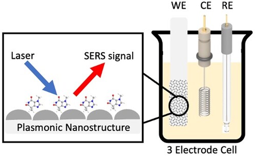
E-SERS is a specific type of SERS which takes place within an EC cell [Citation22,Citation38]. As with a conventional EC cell [Citation39,Citation40], the system contains a working electrode (WE), reference electrode (RE) and counter electrode (CE) and an electrolyte but in E-SERS, the WE is a nanostructured metal surface which can also be used for SERS measurements (Figure ) [Citation22,Citation38]. A potentiostat is used to control the potential of the WE [Citation22].
Figure 3. Schematic diagram of the E-SERS system. SERS spectra are recorded using a three-electrode EC cell containing a WE, RE and CE.
Initially, E-SERS was simply seen as a method of studying EC reactions in situ using Raman spectroscopy [Citation41]. However, it was later found that applying a potential to the WE could actually enhance the SERS signal [Citation22,Citation38]. There are three main reasons for this enhancement.
The first relates to the EC adsorption of analytes on the nanostructured surface. When a charged electrode is in contact with an electrolyte, an interfacial region, known as the EC double layer, will form between the surface and the bulk solution [Citation39]. The nature of this double layer varies depending on the electrode potential. For example, if the electrode potential is more negative than the potential of zero charge, cations will be attracted to the surface and polar molecules such as water will interact with the electrode via their positively charged end [Citation22]. The opposite is true for positive potentials. Consequently, the coverage, adsorption orientation and interaction strength of a target molecule at an electrode can be controlled using the potential [Citation22,Citation42–44]. This is significant because SERS is a surface-selective effect [Citation24] and the magnitude of the SERS signal depends on the proximity of a molecule to the surface [Citation26]. Therefore, increasing the adsorption of a target molecule on the surface will increase its SERS signal.
The second reason for the E-SERS enhancement relates to the number of electrons at the metal surface. Changing the potential of the electrode alters the surface charge density in the plasmonic nanostructure [Citation22]. The surface charge density controls the frequency and amplitude of the surface plasmon resonance which is the reason for the EM SERS enhancement. When a negative potential is applied to the electrode, more electrons are injected into the SERS substrate, increasing the magnitude of the LSPR and consequently the magnitude of the SERS signal.
The third reason is linked to the Fermi level of the metal. The Fermi level determines the likelihood of photon-driven charge transfer between the electrode and the adsorbed molecules [Citation22]. Charge transfer processes play an important part in the chemical enhancement of the SERS signal. Changing the potential of the electrode alters the Fermi level of the metal which can increase the probability of charge transfer between the electrode and the adsorbed molecules [Citation44,Citation45]. An increase in charge transfer processes can lead to an enhancement in the SERS signal.
The relative importance of these three phenomena depends on the system. The structure and composition of the electrode, the analyte, the electrolyte and the environment all affect the E-SERS enhancement. Consequently, it can be difficult to establish the factors at play. Much of the research which has helped to illuminate this subject has been performed on very simple or well-studied analytes such as water and rhodamine 6G [Citation46,Citation47].
The interest in E-SERS is not simply due to the increased SERS signal. It is a powerful technique because it can control which species adsorb onto the surface and how their SERS signal is enhanced. This could enable multiplexing through the detection of different molecules at different potentials. Therefore, increasing the possibility of using SERS to detect biomarkers in complex biological fluids.
Review methodology
The aim of this review is to evaluate the nanostructured electrodes (NSEs) that have been used for E-SERS and identify the most promising approaches. The NSE is a critical part of the E-SERS system because it determines the magnitude of the Raman signal enhancement. Since the 1970s, there have been thousands of papers on the fabrication of nanostructures for SERS which have been extensively reviewed [Citation18,Citation24,Citation26,Citation48–51]. To avoid repetition, this review will focus on NSEs that have been used for E-SERS and will only highlight SERS nanostructures that have the potential to significantly advance E-SERS research.
Requirements for E-SERS NSEs
Before evaluating the literature, it is useful to identify the requirements for an E-SERS NSE. One of the most important features of E-SERS is that the same set-up can be used for EC measurements [Citation39,Citation52] (e.g. cyclic voltammetry and square-wave voltammetry), conventional SERS and E-SERS (SERS with an applied potential). This multipurpose system can therefore extract a lot of useful data and enables sophisticated chemical analysis. However, this also means that the NSE must be suitable for all of these methods. The key features of an E-SERS NSE are as follows:
Plasmonic resonance in the visible/near-infrared range (∼400 to 1000 nm) [Citation26]. Generally, this is the case when the real part of the dielectric function (Re(ϵ)) is negative and the imaginary part (Im(ϵ)) is small [Citation48]. Gold, silver and copper all fulfil these criteria [Citation48].
EC stability. This is why gold is a very popular NSE material [Citation24,Citation48].
Feature size that is less than ∼100 nm [Citation26]. Particularly large EFs can be achieved when ‘hot spots’ are formed between two NPs or at sharp edges or tips [Citation24].
A regular structure that can be reproducibly fabricated to give consistent results [Citation24].
Large surface area to allow many molecules to adsorb onto the surface at once [Citation26].
Fast electron transfer kinetics [Citation40].
Using the EF or limit of detection to evaluate SERS substrates
Throughout this review, the SERS EF or lowest concentration of an analyte detected are quoted as a way of quantifying the performance of a substrate. Although these are the typical metrics used to evaluate SERS nanostructures, they should be treated with caution [Citation26]. The SERS EF is determined experimentally by measuring the intensity of the SERS signal for an absorbed molecule on the metal surface, relative to the intensity of normal Raman signal of the same ‘free’ molecule in solution [Citation24]. The two intensities must be normalised by the number of molecules either on the surface (SERS) or in the solution (conventional Raman) [Citation24]. Issues arise due to difficulties in calculating the number of molecules on the surface and the fact that some researchers calculate the EF based on signals produced at ‘hot spots’ on the metal surface rather than the average signal across the substrate [Citation26]. This can make it difficult to compare work because papers often do not contain details of how the EF is calculated.
Comparing the lowest concentration of an analyte detected can also cause problems because some molecules are much better Raman scatterers than others [Citation26]. For example, dye molecules such as rhodamine 6G exhibit very large ‘resonant Raman scattering’, so being able to detect µM levels of these molecules is less significant than being able to detect the same concentrations of another non-resonant molecule.
The most effective way to evaluate a novel NSE is to perform SERS measurements for the new NSE and a traditional NSE in the same way, using the same analyte and equipment. This review has tried to include this information if it is available in the papers being reviewed.
NSEs
Electrochemically roughened electrodes
The first E-SERS measurements were performed using electrochemically roughened silver electrodes [Citation21]. In this process, successive EC oxidation and reduction cycles are used to create a nanostructured metal surface [Citation38,Citation49]. Initially, a positive potential is applied to the electrode to form soluble ions or an insoluble surface complex, then a negative potential is used to reduce these species, resulting in a randomly, roughened metal surface (Figure ) [Citation38]. The established methods for electrochemically roughening gold, silver and platinum are described by Wu et al [Citation22]. For gold electrodes, the procedure is as follows: first, the surface is cleaned electrochemically in 0.1 mol/L H2SO4 solution and rinsed with ultrapure water. The electrode is then placed in 0.1 mol/L KCl and held at −0.3 V until the current is stable. Next, the potential is scanned to 1.2 V at 1 V/s, set for 1.2 s to allow oxidation and then scanned back to −0.3 V at 0.5 V/s and set for 30 s to allow reduction. The cycle is repeated for at least 15 min to produce a roughened surface [Citation22,Citation53].
Figure 4. Scanning electron microscopy (SEM) images of electrochemically roughened Au films held at 1.2 V in 0.1 M KCl for different numbers of cycles: (a) 3 cycles, (b) 5 cycles and (c) 12 cycles. Adapted from Ref. [Citation54] with permission. Copyright 2020 Elsevier.
![Figure 4. Scanning electron microscopy (SEM) images of electrochemically roughened Au films held at 1.2 V in 0.1 M KCl for different numbers of cycles: (a) 3 cycles, (b) 5 cycles and (c) 12 cycles. Adapted from Ref. [Citation54] with permission. Copyright 2020 Elsevier.](/cms/asset/329d0615-b8d1-4eef-aeaa-159ca1f71706/ymst_a_2197729_f0004_ob.jpg)
Despite their initial success, SERS research has moved away from electrochemically roughed electrodes since the early-2000s [Citation22]. The structures are random and contain features from the angstrom to micron scale [Citation49]. This means the SERS enhancement varies across the surface and between electrodes [Citation38]. However, there are some recent examples of EC roughening being used as a quick, easy, in situ method of E-SERS substrate fabrication [Citation55–58]. This approach is particularly suited to E-SERS because the same set-up can be used for surface preparation and analyte detection. Martín-Yerga et al. electrochemically activated silver screen-printed electrodes (SPEs) in situ whilst simultaneously performing E-SERS of a probe molecule [Citation55]. They were able to quantitatively detect nM levels of ferricyanide and tris(bipyridine)ruthenium (II) [Citation55].
Colloidal NPs deposited on rigid substrates
Colloidal NPs synthesised via wet chemistry are a staple of SERS [Citation59–62]. Gold NPs can be cheaply and reproducibly synthesised using techniques such as the Turkevich–Frens method [Citation59–61]. In this method, tetracholoauric acid (HAuCl4) is reduced by sodium citrate in water, with citrate also acting as an electrostatic stabiliser [Citation59,Citation60]. By carefully controlling the nucleation and growth steps, NPs with defined diameters between 10 and 200 nm ±10% can be synthesised [Citation61]. Silver NPs can be synthesised using a similar citrate reduction of silver nitrate (AgNO3) [Citation63].
Colloidal NPs can be used in E-SERS by drop-casting or spin coating them onto a rigid conductive electrode (e.g. glassy carbon, indium tin oxide (ITO) or gold). Compared to electrochemically roughened electrodes, the surface features are much more uniform in size and the surface signal difference across the whole surface can be less than 10% (Figure ) [Citation22]. This approach has been used successfully in a number of E-SERS sensors [Citation46,Citation64–73].
Figure 5. (a) SEM image of a multi-layered drop-cast Au/Ag NP electrode prepared on a SPE by Zhao et al. Inset: Schematic of the layered structure. (b) E-SERS spectra recorded using the multilayer Au/Ag electrode for 0.5 mM uric acid in 0.1 M NaF supporting electrolyte. Adapted from Ref. [Citation67] with permission. Copyright 2015 American Chemical Society.
![Figure 5. (a) SEM image of a multi-layered drop-cast Au/Ag NP electrode prepared on a SPE by Zhao et al. Inset: Schematic of the layered structure. (b) E-SERS spectra recorded using the multilayer Au/Ag electrode for 0.5 mM uric acid in 0.1 M NaF supporting electrolyte. Adapted from Ref. [Citation67] with permission. Copyright 2015 American Chemical Society.](/cms/asset/bc69afbf-739c-46e4-939f-aa2ecfe0c6d6/ymst_a_2197729_f0005_oc.jpg)
Goodall et al. developed an E-SERS system for the detection of uric acid in urine, an early indicator of preeclampsia in pregnant women [Citation66]. They synthesised silver NPs using a standard citrate reduction (Lee and Meisel method [Citation63]) and then drop-coated them onto a commercially available carbon SPE. The electrode was placed into an EC cell containing 1.0 mM of uric acid in urine simulant and the SERS signal was measured at potentials between 0 and −1 V. The most intense uric acid peaks were observed at −0.8 V vs. Ag/AgCl. At this potential, uric acid concentrations below 0.4 mM were easily identified [Citation66]. Quantitative detection was not achieved in this work but two years later, the same group reported quantitative detection of uric acid at concentrations between 0.1 and 1 mM using a multi-layered Au/Ag NP electrode [Citation67]. Although these detected concentrations are not particularly low compared to other SERS-based sensors, they are good enough to pass the threshold for a preeclampsia diagnostic test (0.4 mM of uric acid). This demonstrates that it is not always necessary to develop the most sensitive sensor possible but rather the most effective system for the application.
Spherical NPs are highly reproducible and cost-effective but only have moderate signal enhancement due to their high symmetry [Citation18,Citation32,Citation74]. More advanced NP shapes which amplify the Raman signal through hotspots at tips and edges are the focus of intense research [Citation18,Citation24]. There are now many papers and reviews which discuss different NPs for SERS including nanorods, nanocubes, nanostars and NFs [Citation18,Citation22,Citation35–37,Citation75]. So far all of the published work on colloidal NPs in E-SERS has used spherical NPs. However, given the attention anisotropic particles have received in SERS research, it seems likely that E-SERS will also start to investigate non-spherical NPs to enhance the Raman signal.
The main problem with depositing colloidal NPs on rigid substrates is the non-uniform distribution of the particles on the surface which limits the SERS enhancement [Citation22]. Some methods have been developed to arrange the NPs in a regular pattern [Citation18,Citation76,Citation77]. Wang et al. produced highly ordered NP arrays with sub-10-nm gaps through the self-assembly of cetrimonium bromide (CTAB)-capped gold NPs (Figure ) [Citation76]. CTAB is a surfactant which forms a bilayer around the Au NP. This bilayer leads to a net positive charge on the NP surface which results in a repulsive force between the NPs that prevents aggregation. Empirical EFs above 1 × 10⁸ were observed for p-mercaptoaniline under near infrared (785 nm) excitation [Citation76]. However, one of the issues with using CTAB-capped NPs is that it is necessary to remove some of the surfactant molecules to allow the analyte of interest to reach the NP surface [Citation77]. More recently, Smith and Lipkowski fabricated a reproducible 2D array of Au NPs by coating gold NPs in SiO2, arranging them on a gold substrate, dissolving the SiO2 and then electrochemically cleaning the substrate [Citation77]. This resulted in a monolayer of bare Au NPs with a regular spacing that was twice the SiO2 shell thickness (4.2 ± 0.7 nm) [Citation77].
Figure 6. (a) Fabrication process used by Wang et al. to produce NP arrays through the self-assembly of CTAB-capped gold NPs. (b) SEM images of Au NP array. Adapted from Ref. [Citation76] with permission. Copyright 2005 American Chemical Society.
![Figure 6. (a) Fabrication process used by Wang et al. to produce NP arrays through the self-assembly of CTAB-capped gold NPs. (b) SEM images of Au NP array. Adapted from Ref. [Citation76] with permission. Copyright 2005 American Chemical Society.](/cms/asset/8e004f56-e631-4efb-aa38-50cc75c6a9cd/ymst_a_2197729_f0006_oc.jpg)
Electrochemical deposition of plasmonic metal NPs
NSEs can also be fabricated via electrochemical deposition (ED) [Citation78–89]. In this method, solid metal NPs are deposited onto a WE from a solution of ions through the application of a positive potential [Citation90]. The reduction of the metal ions can be represented by
(2)
(2)
Like EC roughening, ED requires a three-electrode EC cell and a potentiostat [Citation90]. This makes it an attractive fabrication process for E-SERS because it uses much of the same equipment. It also has the potential to be quicker and easier than using colloidal NPs because the NPs are deposited straight onto a rigid, conductive substrate, removing the need for drop-coating.
Dai and Compton first electrodeposited gold NPs onto ITO in 2006 [Citation86]. They used 0.1 mM of HAuCl4 in 0.5 M H2SO4 as their electrolyte and applied a potential step from +1.055 V to −0.045 V (vs. saturated calomel electrode) for a fixed time (15, 50, 150 or 300 s). Varying the experimental parameters revealed (unsurprisingly) that the particle size increased with concentration and deposition time. They also found that for 0.1 mM HAuCl4 applying 20 cycles of 15 s led to more monodisperse particles than a single potential step of 300 s (165 ± 30 nm vs. 154 ± 68 nm) [Citation86].
Wang et al. refined Dai and Compton’s method in 2013 using a two-step approach (Figure ) [Citation79]. First, they applied a potential step from +0.89 V to −0.8 V (vs. a saturated calomel electrode) to an ITO WE in a solution containing 0.1 mM HAlCl4 and 0.1 M NaClO4 for 10 s. This step triggers the formation of many small gold NPs (mean diameter of 9 ± 2 nm and particle density of 1800 ± 200 particles per µm2). These NPs then act as seeds in the subsequent growth step due to the preferential reduction and deposition of on existing gold particles. The NPs are grown in the same EC cell using cyclic voltammetry. The potential is scanned between +0.3 V and −0.04 V at 50 mV/s for a defined number of cycles. As the number of cycles increases, the size of the particles increases, and the density decreases. Importantly for SERS, the gap between the adjacent NPs also decreases, resulting in the formation of ‘hot spots’. Five hundred deposition cycles resulted in NPs with a mean diameter of 50 ± 9 nm and nanogap distances of <10 nm [Citation79]. These particles are significantly smaller, more uniform and closer spaced than those made by Dai and Compton [Citation86]. In some ways, ED can be seen as an extension of EC roughening. The process and chemicals are slightly more complicated, but the nanostructures formed are significantly more uniform making it a very attractive fabrication method for E-SERS electrodes.
Figure 7. The two-step ED process used by Wang et al. to form gold NPs on ITO. Reproduced from Ref [Citation79] with permission. Copyright 2013 American Chemical Society.
![Figure 7. The two-step ED process used by Wang et al. to form gold NPs on ITO. Reproduced from Ref [Citation79] with permission. Copyright 2013 American Chemical Society.](/cms/asset/f926215a-4445-4da4-8b72-8d969414eb62/ymst_a_2197729_f0007_oc.jpg)
As discussed ealier, anisotropic NPs can display enhanced SERS signals due to ‘hot spots’ which form at edges or tips. The electrodeposited NPs discussed so far have all been spherical but there have been some attempts to ED non-spherical NPs [Citation80,Citation85,Citation88,Citation91–93]. Flower-like nanostructures (NFs) can display high SERS EFs due to the nanogaps that form between their ‘petals’ [Citation80].
Ye et al. electrodeposited gold NFs onto ITO from a solution of 2 mM HAuCl4 and 0.1 M KNO3 at a constant potential of −0.1 V [Citation80]. The ITO electrodes were coated with polydopamine (Pdop), a multifunctional biopolymer, which triggered the formation of Au NFs. The reason for the change in morphology is not completely clear but Ye et al. do show that the Pdop increases the nucleation rate of the gold NPs [Citation80]. They studied the SERS response of the nanostructures using rhodamine 6G as a probe molecule and found that the Raman peaks were significantly larger for the NFs than the NPs [Citation80].
NSEs fabricated using template-based methods
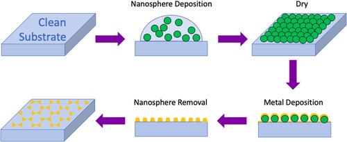
Despite being able to regulate the size of colloidal and electrochemically deposited NPs, it is still difficult to control the spaces between them [Citation22]. This leads to variation in the SERS enhancement because ‘hot spots’ formed at the gaps between NPs play a vital role in signal amplification [Citation24]. Template-based methods can be used to create very ordered NSEs with controlled inter-particle spacing [Citation22]. The most popular template-based method in SERS research is nanosphere lithography (NSL) which was proposed by Hulteen and Van Duyne in 1995 [Citation94]. This procedure is demonstrated in Figure . First, monodisperse polystyrene or SiO2 nanospheres with a chosen diameter are placed onto a substrate and allowed to self-assemble into a close-packed hexagonal array [Citation95,Citation96]. The substrate should be thoroughly cleaned, and, for E-SERS, it must also be conductive (e.g. ITO or metal coated glass) [Citation22]. Next, a thin layer (15–100 nm) of metal is deposited by physical vapour deposition on top of the spheres [Citation95]. The nanospheres are then washed away leaving a uniform triangular NP array on the surface.
Figure 8. The NSL fabrication process. Monodisperse nanospheres are deposited onto a substrate and allowed to self-assemble into a close-packed hexagonal array. Then, a thin layer of metal is deposited by physical vapour deposition on top of the spheres. The nanospheres are washed away leaving a uniform triangle NP array.
The basic NSL method described above can be modified in different ways to produce the desired nanostructured surface [Citation97,Citation98]. For example, Zhang et al. were able to modify the shape of NSL-fabricated silver triangles on ITO using EC oxidation [Citation98]. A potential step from +200 mV to +400 mV was applied to the nanotriangles which selectively oxidised the triangles, first at the bottom edges, then at the tips and finally from the top face [Citation98]. Applying multiple cycles resulted in a regular array of spherical NPs (Figure ).
Figure 9. Ag NPs on ITO produced by Zhang et al. using NSL. (a) SEM images of Ag NP array produced using nanospheres with a 590-nm diameter. (b) The LSPR λmax of the Ag NPs shift towards shorter wavelengths after applying a potential step. Atomic force microscope images of a NP (c) before any EC measurements, (d) after one cycle and (e) after two cycles. Adapted from Ref. [Citation98] with permission. Copyright 2005 American Chemical Society.
![Figure 9. Ag NPs on ITO produced by Zhang et al. using NSL. (a) SEM images of Ag NP array produced using nanospheres with a 590-nm diameter. (b) The LSPR λmax of the Ag NPs shift towards shorter wavelengths after applying a potential step. Atomic force microscope images of a NP (c) before any EC measurements, (d) after one cycle and (e) after two cycles. Adapted from Ref. [Citation98] with permission. Copyright 2005 American Chemical Society.](/cms/asset/37c2821b-4862-4b21-bc15-a4a0b5435b19/ymst_a_2197729_f0009_oc.jpg)
Van Duyne’s group also developed another NSL method called ‘film over nanosphere’ (FON) [Citation95,Citation99,Citation100]. In this method, a thicker metal layer (∼200 nm) is deposited on top of the polystyrene or SiO2 nanospheres and, unlike tradition NSL, they are not removed. This results in a very uniform rough surface [Citation99]. Zhang et al. used silver FON electrodes to perform E-SERS measurements of pyridine and the Ru(bpy)3+/Ru(bpy)2+ complexes as well as dipicolinic acid (DPA), an anthrax bacterial endospore marker [Citation101]. They were able to detect 8 × 10⁻⁵ M of DPA in 5 min [Citation101]. This was a significant improvement on the results achieved using a traditional electrochemically roughened silver electrode. Despite the many benefits of NSL, the complexity of the process leads to several drawbacks. Physical vapour deposition requires expensive, specialist equipment and a significant amount of the deposited gold or silver is wasted when the nanospheres are washed away. The number of steps also makes the process quite time-consuming and costly.
In the early-2000s, Bartlett and his colleagues developed a version of NSL which did not rely on expensive, specialist vapour deposition equipment [Citation102,Citation103]. The sphere segment void (SSV) method uses the same hexagonal arrangement of uniform nanospheres but instead of depositing a metal film on top of the spheres, the metal is electrodeposited onto the substrate between the nanospheres [Citation102,Citation104]. Removing the spheres results in a thin structured film containing a regular hexagonal array of uniform voids [Citation22,Citation102]. The size of the voids can be controlled by varying the thickness of the film. Figure shows a copper/silver SSV surface fabricated using 1 µm diameter spheres.
Figure 10. (a) SEM image of a polystyrene monolayer film used for the SSV method. (b) and (c) SEM images of the resulting Cu/Ag SSVs. Adapted from Ref. [Citation105] with permission. Copyright 2019 American Chemical Society.
![Figure 10. (a) SEM image of a polystyrene monolayer film used for the SSV method. (b) and (c) SEM images of the resulting Cu/Ag SSVs. Adapted from Ref. [Citation105] with permission. Copyright 2019 American Chemical Society.](/cms/asset/cfb8d946-a218-4f5a-a827-ecd6e55cd310/ymst_a_2197729_f0010_ob.jpg)
The SSV method is an attractive electrode fabrication technique for E-SERS because it uses the same equipment needed for the EC measurements. There have been a number of successful attempts to use SSV for E-SERS [Citation104,Citation106–108]. For example, Abdelsalam et al. fabricated SSV structured silver surfaces and used them to study the oxidation and reduction of a flavin analogue (isoalloxazine) [Citation107]. The SSV surfaces gave stable, reproducible surface enhancements at a range of electrode potentials and the spectra were sensitive to sub-femtomole quantities of immobilised flavin [Citation107]. SSV is cheaper than conventional NSL because it does not require expensive vacuum chambers and less metal is wasted during fabrication. However, it is still a time-consuming multi-step process which could mean it is unsuitable for use in commercial sensors.
Electron beam lithography is another technique that can be used to create NPs with precise sizes, shapes and spacings [Citation95,Citation109]. In this method, a substrate is coated with an electron sensitive polymer film (or resist) and then a focussed beam of electrons is used to draw custom shapes in the film [Citation110,Citation111]. The electron beam changes the solubility of the polymer allowing either the exposed or unexposed areas of the resist to be dissolved, resulting in a patterned mask. A metal film is then deposited on top of this mask and the polymer is washed away, leaving behind a nanostructured metal surface [Citation95,Citation110]. This method can create uniform nanostructures with dimensions below 10 nm but again, it is expensive and time-consuming [Citation110,Citation112]. The equipment required is even more expensive and specialist than that which is needed for NSL. As such, it is not practical to use this technique in industry, but it can be utilised in fundamental EC research [Citation44,Citation113].
Oyamada et al. fabricated well-defined gold dimer structures with a gap distance of 2.5 nm using electron beam lithography [Citation44]. They used these nanostructures to conduct E-SERS measurements of two structural isomers, 4,4′-bipyridine (44bpy) and 2,2′-bipyridine (22bpy), at different applied potentials. They found that the Raman signals increased for both of the molecules at negative potentials. However, when they used a mixed solution of 44bpy and 22bpy, the signal for 44bpy was larger at positive potentials and the signal for 22bpy was larger at negative potentials, showing that the dominant absorbent could be controlled using the electrode potential [Citation44]. This type of fundamental research helps to shed light on the complex EC interactions which take place at electrode surfaces [Citation42].
The E-SERS electrode fabrication methods reported in the literature are classified in Table , along with the nanostructure size and shape produced, and the analyte detected.
Table 1. Classification of the E-SERS electrode fabrication methods reported in the literature.
Analyte detection with E-SERS
Although E-SERS has not been studied as extensively as conventional SERS, the literature contains examples of it being used to identify a range of analytes. These include therapy drugs [Citation71,Citation100,Citation116,Citation118], biomarkers [Citation56,Citation66–68,Citation104,Citation107] and food contaminates [Citation57,Citation70,Citation119]. The analytes studied and the fabrication methods used to make the E-SERS electrodes are detailed in Table . Despite the success detecting a variety of analytes, very few of these studies demonstrate quantitative detection. Reliable quantitative measurements rely on robust, repeatable NSEs which can be difficult to fabricate. Issues also arise due to the complex nature of the E-SERS system, in particular the important part surface adsorption plays in the detection of analytes. However, successful quantitative detection has been achieved. The E-SERS studies reported in the literature are summarised in Table with details of the electrode fabrication method and, if quantitative analysis was performed, the limit of detection and detection range.
Table 2. Current state-of-the-art in E-SERS analyte detection reported in the literature.
Outlook and conclusion
The aim of this review was to determine the most effective method of fabricating a NSE for E-SERS. To do this, it was necessary to define the requirements of such an electrode. These were identified as gold or silver nanoscale features; a regular structure with uniform nanogaps between features; fast electron transfer kinetics; a large surface area and a repeatable, reliable fabrication process. On top of this, there were practical considerations such as the ease, cost and length of the manufacture procedure. Currently, the most commonly used approaches fell into four main categories: EC roughening, colloidal NP deposition, ED and template-based methods. The assessment of these methods can be summarised very simply as: electrodes with large, repeatable SERS enhancements can be made but the processes are expensive and time-consuming; easier, quicker methods can also be used to create effective substrates, but they are much less uniform and reliable. Consequently, to determine the most effective fabrication method, one must consider the application.
In the case of biomarker detection, the appropriate substrate depends on the molecule being detected and the concentrations present. If the biomarker is a very effective Raman scatterer or present in high concentrations, an electrode with a lower SERS enhancement could still be part of a successful sensor. Conversely, if a biomarker is difficult to detect and only present at very low concentrations, large SERS signals are needed which would mean choosing a template-based fabrication method. It would also be necessary to consider the cost of the sensor in relation to its use case.
Ultimately, the aim is to develop fabrication methods that combine the qualities of the four approaches to create electrodes which are reliable, sensitive and cost-effective. The key avenues for future research fall into two main categories. The first is to apply the most promising developments from SERS research to E-SERS electrode fabrication. The use of complex shaped nanostructures that have been engineered to maximise ‘hot spots’, such as nanostars, NFs and nanourchins, have exhibited impressive EFs in a range of SERS applications and employing these structures in E-SERS would likely offer improved detection limits [Citation18,Citation22,Citation35–37].
Furthermore, in recent years, heterogeneous nanostructures which contain two or more different materials, such as core–shell and hybrid NPs, have received increased attention [Citation121–124]. Depending on the materials used, they can offer a range of benefits. For example, coating a plasmonic metal in a dielectric material can improve the stability of the NPs [Citation125,Citation126] and coating an inexpensive carrier with a noble metal can reduce the cost of plasmonic NPs [Citation127]. Additionally, certain hybrid particles, such as gold core–silver shell NPs and plasmonic metal–semiconductor NPs, can exhibit charge transfer between the two materials which can lead to boosted SERS enhancements [Citation30,Citation67,Citation128–136].
The second key avenue for future research is to utilise novel nanofabrication techniques to produce carefully controlled nanostructures in quicker and more cost-effective ways than the current template-based techniques. Possible approaches to investigate include nanoscale glancing able deposition [Citation137,Citation138], dip-pen lithography [Citation139] and innovative self-assembly methods [Citation140–142]. Developing a reliable, sensitive and cost-effective E-SERS electrode fabrication method requires innovation and creative thinking but there are already many promising approaches and the potential benefits of early disease detection make it a worthwhile challenge.
Disclosure statement
No potential conflict of interest was reported by the author.
Additional information
Funding
References
- Etzioni R, Urban N, Ramsey S, et al. The case for early detection. Nat Rev Cancer. 2003;3:243–252.
- Yager P, Domingo GJ, Gerdes J. Point-of-care diagnostics for global health. Annu Rev Biomed Eng. 2008;10:107–144.
- FDA-NIH Biomarker Working Group. Diagnostic biomarker. Silver Spring (MD): Food and Drug Administration (US); 2016.
- Hoseok I, Cho J-Y. Chapter three—lung cancer biomarkers. In: Makowski GS, editor. Advances in clinical chemistry. Elsevier; 2015. p. 107–170.
- Simrén J, Elmgren A, Blennow K, et al. Chapter six—fluid biomarkers in Alzheimer’s disease. In: Makowski GS, editor. Advances in clinical chemistry. Elsevier; 2023. p. 249–281.
- Bravo-Merodio L, Acharjee A, Russ D, et al.. Translational biomarkers in the era of precision medicine. In: Makowski G, editor. Advances in clinical chemistry Vol. 102. Cambridge (MA): Elsevier; 2021. p. 191–232.
- Higson S. Analytical chemistry. Oxford: Oxford University Press; 2003.
- Ronkainen NJ, Halsall HB, Heineman WR. Electrochemical biosensors. Chem Soc Rev. 2010;39:1747.
- Shao Y, Zhu Y, Zheng R, et al. Highly sensitive and selective surface molecularly imprinted polymer electrochemical sensor prepared by Au and MXene modified glassy carbon electrode for efficient detection of tetrabromobisphenol A in water. Adv Compos Hybrid Mater. 2022;5:3104–3116.
- Ahmed J, Faisal M, Alsareii SA, et al. Highly sensitive and selective non-enzymatic uric acid electrochemical sensor based on novel polypyrrole-carbon black-Co3O4 nanocomposite. Adv Compos Hybrid Mater. 2022;5:920–933.
- Koczula KM, Gallotta A. Lateral flow assays. Essays Biochem. 2016;60:111–120.
- Naresh V, Lee N. A review on biosensors and recent development of nanostructured materials-enabled biosensors. Sensors. 2021;21:1109.
- Satpathy G, Chandra GK, Elayaraja D, et al. Nanoparticles and bacterial interaction of host-pathogens and the detection enhancement of biomolecules by fluorescence Raman spectroscopic investigation. Eng Sci. 2022;20:341–351.
- Yin H, Zhong W, Yin M, et al. Carboxyl-functionalized poly(arylene ether nitrile)-based rare earth coordination polymer nanofibrous membrane for highly sensitive and selective sensing of Fe3+ ions. Adv Compos Hybrid Mater. 2022;5:2031–2041.
- Cali K, Tuccori E, Persaud KC. Chapter eighteen—gravimetric biosensors. In: Pelosi P, Knoll W, editors. Methods in enzymology. Cambridge (MA): Academic Press; 2020. p. 435–468.
- Go DB, Atashbar MZ, Ramshani Z, et al. Surface acoustic wave devices for chemical sensing and microfluidics: a review and perspective. Anal Methods. 2017;9:4112–4134.
- Peveler WJ, Yazdani M, Rotello VM. Selectivity and specificity: pros and cons in sensing. ACS Sensors. 2016;1:1282–1285.
- Langer J, de Aberasturi DJ, Aizpurua J, et al. Present and future of surface-enhanced Raman scattering. ACS Nano. 2019;14:28–117.
- Vandenabeele P. Practical Raman spectroscopy: an introduction. Chichester: Wiley; 2013.
- Atkins PW, De Paula J. Physical chemistry. Oxford: Oxford University Press; 2006.
- Fleischmann M, Hendra PJ, McQuillan AJ. Raman spectra of pyridine adsorbed at a silver electrode. Chem Phys Lett. 1974;26:163–166.
- Wu D-Y, Li J-F, Ren B, et al. Electrochemical surface-enhanced Raman spectroscopy of nanostructures. Chem Soc Rev. 2008;37:1025.
- Pilot R, Signorini R, Durante C, et al. A review on surface-enhanced Raman scattering. Biosensors. 2019;9:57.
- Schlücker S. Surface-enhanced Raman spectroscopy: concepts and chemical applications. Angew Chem Int Ed. 2014;53:4756–4795.
- Petryayeva E, Krull UJ. Localized surface plasmon resonance: nanostructures, bioassays and biosensing—a review. Anal Chim Acta. 2011;706:8–24.
- Le Ru EC, Etchegoin PG. Principles of surface-enhanced Raman spectroscopy and related plasmonic effects. 1st ed. Boston, MA: Elsevier; 2009.
- Moskovits M. Surface-enhanced Raman spectroscopy: a brief retrospective. J Raman Spectrosc. 2005;36:485–496.
- Xu H, Aizpurua J, Käll M, et al. Electromagnetic contributions to single-molecule sensitivity in surface-enhanced Raman scattering. Phys Rev E. 2000;62:4318–4324.
- Chio W-IK, Liu J, Jones T, et al. SERS multiplexing of methylxanthine drug isomers via host–guest size matching and machine learning. J Mater Chem C. 2021;9:12624–12632.
- Davison G, Jones T, Liu J, et al. Computer-aided design and analysis of spectrally aligned hybrid plasmonic nanojunctions for SERS detection of nucleobases. Adv Mater Technol. 2023:2201400.
- Zhu W, Esteban R, Borisov AG, et al. Quantum mechanical effects in plasmonic structures with subnanometre gaps. Nat Commun. 2016;7:11495.
- Jones T, Davison G, Jeong H-H, et al. Chapter 2. Engineered gold nanoparticles for photothermal applications. In: Ye E, Li Z, editors. Nanoscience & nanotechnology series. Cambridge: Royal Society of Chemistry; 2022. p. 33–80.
- Kelly KL, Coronado E, Zhao LL, et al. The optical properties of metal nanoparticles: the influence of size, shape, and dielectric environment. J Phys Chem B. 2003;107:668–677.
- Hao E, Schatz GC. Electromagnetic fields around silver nanoparticles and dimers. J Chem Phys. 2004;120:357–366.
- Hu J, Jiang R, Zhang H, et al. Colloidal porous gold nanoparticles. Nanoscale. 2018;10:18473–18481.
- Chen X, Jiang C, Yu S. Nanostructured materials for applications in surface-enhanced Raman scattering. CrystEngComm. 2014;16:9959–9973.
- Reguera J, Langer J, Aberasturi DJ, et al. Anisotropic metal nanoparticles for surface enhanced Raman scattering. Chem Soc Rev. 2017;46:3866–3885.
- Tian Z-Q, Zhang X-M. Electrochemical Surface-Enhanced Raman Spectroscopy (EC-SERS): Early History, Principles, Methods, and Experiments. In: Pletcher D, Tian Z-Q, Williams DE, editors. Developments in electrochemistry. 1st ed. Chichester: Wiley; 2014. p. 113–135.
- Compton RG, Laborda E, Ward KR, et al. Understanding voltammetry: simulation of electrode processes. London/Singapore: Imperial College Press/Distributed by World Scientific Pub. Co; 2014.
- Elgrishi N, Rountree KJ, McCarthy BD, et al. A practical beginner’s guide to cyclic voltammetry. J Chem Educ. 2018;95:197–206.
- Alkire RC, Bartlett PN, Lipkowski J. Advances in Electrochemical Science and Engineering: Nanopatterned and Nanoparticle‐Modified Electrodes. 1st ed. Weinheim: Wiley; 2017.
- Willets KA. Probing nanoscale interfaces with electrochemical surface-enhanced Raman scattering. Curr Opin Electrochem. 2019;13:18–24.
- Fu B, Van Dyck C, Zaleski S, et al. Single molecule electrochemistry: impact of surface site heterogeneity. J Phys Chem C. 2016;120:27241–27249.
- Oyamada N, Minamimoto H, Murakoshi K. In situ observation of unique bianalyte molecular behaviors at the gap of a single metal nanodimer structure via electrochemical surface-enhanced Raman scattering measurements. J Phys Chem C. 2019;123:24740–24745.
- Zhou L, Chen X, Ren G, et al. Electrically tunable SERS based on plasmonic gold nanorod-graphene/ion-gel hybrid structure with a low voltage. Carbon N Y. 2022;187:425–431.
- Zaleski S, Cardinal MF, Chulhai DV, et al. Toward monitoring electrochemical reactions with dual-wavelength SERS: characterization of rhodamine 6G (R6G) neutral radical species and covalent tethering of R6G to silver nanoparticles. J Phys Chem C. 2016;120:24982–24991.
- Wang Y-H, Zheng S, Yang W-M, et al. In situ Raman spectroscopy reveals the structure and dissociation of interfacial water. Nature. 2021;600:81–85.
- Schlücker S. Surface enhanced Raman spectroscopy: analytical, biophysical and life science applications. Weinheim: Wiley-VCH Verlag; 2011.
- Tian Z-Q, Ren B, Wu D-Y. Surface-enhanced Raman scattering: from noble to transition metals and from rough surfaces to ordered nanostructures. J Phys Chem B. 2002;106:9463–9483.
- Shi R, Liu X, Ying Y. Facing challenges in real-life application of surface-enhanced Raman scattering: design and nanofabrication of surface-enhanced Raman scattering substrates for rapid field test of food contaminants. J Agric Food Chem. 2018;66:6525–6543.
- Jing Y, Wang R, Wang Q, et al. An overview of surface-enhanced Raman scattering substrates by pulsed laser deposition technique: fundamentals and applications. Adv Compos Hybrid Mater. 2021;4:885–905.
- Bard AJ, Faulkner LR. Electrochemical methods: fundamentals and applications. 2nd ed. New York: Wiley; 2001.
- Gao P, Gosztola D, Leung L-WH, et al. Surface-enhanced Raman scattering at gold electrodes: dependence on electrochemical pretreatment conditions and comparisons with silver. J Electroanal Chem Interfacial Electrochem. 1987;233:211–222.
- Wang J, Qiu C, Mu X, et al. Ultrasensitive SERS detection of rhodamine 6G and p-nitrophenol based on electrochemically roughened nano-Au film. Talanta. 2020;210:120631.
- Martín-Yerga D, Pérez-Junquera A, González-García MB, et al. Quantitative Raman spectroelectrochemistry using silver screen-printed electrodes. Electrochim Acta. 2018;264:183–190.
- Zhu Z, Yoshikawa H, Saito M, et al. Fabrication of surface-enhanced Raman spectroscopy (SERS)—active electrodes by silver sputtering deposition for electrochemical SERS analysis. Electroanalysis. 2018;30:1432–1437.
- Ibáñez D, Pérez-Junquera A, González-García MB, et al. Spectroelectrochemical elucidation of B vitamins present in multivitamin complexes by EC-SERS. Talanta. 2020;206:120190.
- Martín-Yerga D, Pérez-Junquera A, Hernández-Santos D, et al. In situ activation of thick-film disposable copper electrodes for sensitive detection of malachite green using electrochemical surface-enhanced Raman scattering (EC-SERS). Electroanalysis. 2018;30:1095–1099.
- Turkevich J, Stevenson PC, Hillier J. A study of the nucleation and growth processes in the synthesis of colloidal gold. Discuss Faraday Soc. 1951;11:55–75.
- Frens G. Controlled nucleation for the regulation of the particle size in monodisperse gold suspensions. Nat Phys Sci. 1973;241:20–22.
- Bastús NG, Comenge J, Puntes V. Kinetically controlled seeded growth synthesis of citrate-stabilized gold nanoparticles of up to 200 nm: size focusing versus Ostwald ripening. Langmuir. 2011;27:11098–11105.
- Chio W-IK, Davison G, Jones T, et al. Quantitative SERS detection of uric acid via formation of precise plasmonic nanojunctions within aggregates of gold nanoparticles and cucurbit[n]uril. JoVE. 2020;164:e61682–e61697.
- Lee PC, Meisel D. Adsorption and surface-enhanced Raman of dyes on silver and gold sols. J Phys Chem. 1982;86:3391–3395.
- Cortés E, Etchegoin PG, Le Ru EC, et al. Monitoring the electrochemistry of single molecules by surface-enhanced Raman spectroscopy. J Am Chem Soc. 2010;132:18034–18037.
- Zong C, Chen C-J, Zhang M, et al. Transient electrochemical surface-enhanced Raman spectroscopy: a millisecond time-resolved study of an electrochemical redox process. J Am Chem Soc. 2015;137:11768–11774.
- Goodall BL, Robinson AM, Brosseau CL. Electrochemical-surface enhanced Raman spectroscopy (E-SERS) of uric acid: a potential rapid diagnostic method for early preeclampsia detection. Phys Chem Chem Phys 2013;15:1382–1388.
- Zhao L, Blackburn J, Brosseau CL. Quantitative detection of uric acid by electrochemical-surface enhanced Raman spectroscopy using a multilayered Au/Ag substrate. Anal Chem. 2015;87:441–447.
- Smith SR, Seenath R, Kulak MR, et al. Characterization of a self-assembled monolayer of 1-thio-β-d-glucose with electrochemical surface enhanced Raman spectroscopy using a nanoparticle modified gold electrode. Langmuir. 2015;31:10076–10086.
- Lynk TP, Sit CS, Brosseau CL. Electrochemical surface-enhanced Raman spectroscopy as a platform for bacterial detection and identification. Anal Chem. 2018;90:12639–12646.
- Robinson AM, Harroun SG, Bergman J, et al. Portable electrochemical surface-enhanced Raman spectroscopy system for routine spectroelectrochemical analysis. Anal Chem. 2012;84:1760–1764.
- Bindesri SD, Alhatab DS, Brosseau CL. Development of an electrochemical surface-enhanced Raman spectroscopy (EC-SERS) fabric-based plasmonic sensor for point-of-care diagnostics. Analyst. 2018;143:4128–4135.
- Yu WW, White IM. Inkjet-printed paper-based SERS dipsticks and swabs for trace chemical detection. Analyst. 2013;138:1020–1025.
- Robinson AM, Zhao L, Shah Alam MY, et al. The development of ‘fab-chips’ as low-cost, sensitive surface-enhanced Raman spectroscopy (SERS) substrates for analytical applications. Analyst. 2015;140:779–785.
- Jeong H-H, Choi E, Ellis E, et al. Recent advances in gold nanoparticles for biomedical applications: from hybrid structures to multi-functionality. J Mater Chem B. 2019;7:3480–3496.
- Silvestri A, Lay L, Psaro R, et al. Fluidic manufacture of star-shaped gold nanoparticles. Chem Eur J. 2017;23:9732–9735.
- Wang H, Levin CS, Halas NJ. Nanosphere arrays with controlled Sub-10-nm gaps as surface-enhanced Raman spectroscopy substrates. J Am Chem Soc. 2005;127:14992–14993.
- Smith SR, Lipkowski J. Guided assembly of two-dimensional arrays of gold nanoparticles on a polycrystalline gold electrode for electrochemical surface-enhanced Raman spectroscopy. J Phys Chem C. 2018;122:7303–7311.
- Dai X, Nekrassova O, Hyde ME, et al. Anodic stripping voltammetry of arsenic(III) using gold nanoparticle-modified electrodes. Anal Chem. 2004;76:5924–5929.
- Wang J, Cao X, Li L, et al. Electrochemical seed-mediated growth of surface-enhanced Raman scattering active Au(111)-like nanoparticles on indium tin oxide electrodes. J Phys Chem C. 2013;117:15817–15828.
- Ye W, Wang D, Zhang H, et al. Electrochemical growth of flowerlike gold nanoparticles on polydopamine modified ITO glass for SERS application. Electrochim Acta. 2010;55:2004–2009.
- Dendisová M., Němečková Z, Člupek M, et al. EC-SERS study of phenolic acids sorption behavior on Au, Ag and Cu substrates—effect of applied potential and metal used. Appl Surf Sci. 2019;470:716–723.
- Clarke OJR S, Marie GJH, Brosseau CL. Evaluation of an electrodeposited bimetallic Cu/Ag nanostructured screen printed electrode for electrochemical surface-enhanced Raman spectroscopy (EC-SERS) investigations. J Electrochem Soc. 2017;164:B3091–B3095.
- Tsai M-H, Lin Y-K, Luo S-C. Electrochemical SERS for in situ monitoring the redox states of PEDOT and its potential application in oxidant detection. ACS Appl Mater Interfaces. 2019;11:1402–1410.
- Dong P, Lin Y, Deng J, et al. Ultrathin gold-shell coated silver nanoparticles onto a glass platform for improvement of plasmonic sensors. ACS Appl Mater Interfaces. 2013;5:2392–2399.
- Bian J, Shu S, Li J, et al. Reproducible and recyclable SERS substrates: flower-like Ag structures with concave surfaces formed by electrodeposition. Appl Surf Sci. 2015;333:126–133.
- Dai X, Compton RG. Direct electrodeposition of gold nanoparticles onto indium tin oxide film coated glass: application to the detection of arsenic(III). Anal Sci. 2006;22:567–570.
- Ibáñez D, González-García MB, Hernández-Santos D, et al. Detection of dithiocarbamate, chloronicotinyl and organophosphate pesticides by electrochemical activation of SERS features of screen-printed electrodes. Spectrochim Acta Part A. 2021;248:119174.
- Cheng Z-Q, Li Z-W, Xu J-H, et al. Morphology-controlled fabrication of large-scale dendritic silver nanostructures for catalysis and SERS applications. Nanoscale Res Lett. 2019;14:89.
- Subhadarshini S, Singh R, Goswami DK, et al. Electrodeposited Cu2O nanopetal architecture as a superhydrophobic and antibacterial surface. Langmuir. 2019;35:17166–17176.
- Paunovic M, Schlesinger M. Fundamentals of electrochemical deposition. Hoboken (NJ): Wiley; 2006.
- Su S, Wu Y, Zhu D, et al. On-electrode synthesis of shape-controlled hierarchical flower-like gold nanostructures for efficient interfacial DNA assembly and sensitive electrochemical sensing of MicroRNA. Small. 2016;12:3794–3801.
- Tang S, Meng X, Wang C, et al. Flowerlike Ag microparticles with novel nanostructure synthesized by an electrochemical approach. Mater Chem Phys. 2009;114:842–847.
- Bian J-C, Chen Z-D, Li Z, et al. Electrodeposition of hierarchical Ag nanostructures on ITO glass for reproducible and sensitive SERS application. Appl Surf Sci. 2012;258:6632–6636.
- Hulteen JC, Van Duyne RP. Nanosphere lithography: a materials general fabrication process for periodic particle array surfaces. J Vacuum Sci Technol A: Vacuum Surfaces Films. 1995;13:1553–1558.
- Willets KA, Van Duyne RP. Localized surface plasmon resonance spectroscopy and sensing. Annu Rev Phys Chem. 2007;58:267–297.
- Zhang X, Yonzon CR, Van Duyne RP. Nanosphere lithography fabricated plasmonic materials and their applications. J Mater Res. 2006;21:1083–1092.
- Li X, McNaughter PD, O’Brien P, et al. Photoelectrochemical formation of polysulfide at PbS QD-sensitized plasmonic electrodes. J Phys Chem Lett. 2019;10:5357–5363.
- Zhang X, Hicks EM, Zhao J, et al. Electrochemical tuning of silver nanoparticles fabricated by nanosphere lithography. Nano Lett. 2005;5:1503–1507.
- Dick LA, McFarland AD, Haynes CL, et al. Metal film over nanosphere (MFON) electrodes for surface-enhanced Raman spectroscopy (SERS): improvements in surface nanostructure stability and suppression of irreversible loss. J Phys Chem B. 2002;106:853–860.
- Zaleski S, Clark KA, Smith MM, et al. Identification and quantification of intravenous therapy drugs using normal Raman spectroscopy and electrochemical surface-enhanced Raman spectroscopy. Anal Chem. 2017;89:2497–2504.
- Zhang X, Yonzon CR, Duyne RPV. An electrochemical surface-enhanced Raman spectroscopy approach to anthrax detection. Plasmonics: Metal Nanostruct Opt Properties Int Soc Opt Photonics. 2003;5221:82–91.
- Bartlett PN, Baumberg JJ, Coyle S, et al. Optical properties of nanostructured metal films. Faraday Disc. 2004;125:117.
- Mahajan S, Abdelsalam M, Suguwara Y, et al. Tuning plasmons on nano-structured substrates for NIR-SERS. Phys Chem Chem Phys 2007;9:104–109.
- Bassetto VC, Russell AE, Kubota LT, et al. Preparation of copper sphere segment void templates for electrochemical SERS and their use to study the interaction of amino acids with copper under potentiostatic control. Electrochim Acta. 2014;144:400–405.
- Dong X, Ohnoutek L, Yang Y, et al. Cu/Ag sphere segment void array as efficient surface enhanced Raman spectroscopy substrate for detecting individual atmospheric aerosol. Anal Chem. 2019;91:13647–13657.
- Abdelsalam ME, Bartlett PN, Baumberg JJ, et al. Electrochemical SERS at a structured gold surface. Electrochem Commun. 2005;7:740–744.
- Abdelsalam M, Bartlett PN, Russell AE, et al. Quantitative electrochemical SERS of flavin at a structured silver surface. Langmuir. 2008;24:7018–7023.
- Vezvaie M, Brosseau CL, Lipkowski J. Electrochemical SERS study of a biomimetic membrane supported at a nanocavity patterned Ag electrode. Electrochim Acta. 2013;110:120–132.
- Peters RF, Gutierrez-Rivera L, Dew SK, et al. Surface enhanced Raman spectroscopy detection of biomolecules using EBL fabricated nanostructured substrates. JoVE. 2015;97:e52712–e52729.
- Chen Y. Nanofabrication by electron beam lithography and its applications: A review. Microelectronic Engineering. 2015;135:57–72.
- Prakash S, Yeom J. Advanced fabrication methods and techniques. In: Prakash S, Yeom J, editors. Nanofluidics and Microfluidics. Waltham (MA): Elsevier; 2014. p. 87–170.
- Abu Hatab NA, Oran JM, Sepaniak MJ. Surface-enhanced Raman spectroscopy substrates created via electron beam lithography and nanotransfer printing. ACS Nano. 2008;2:377–385.
- Ward DR, Grady NK, Levin CS, et al. Electromigrated nanoscale gaps for surface-enhanced Raman spectroscopy. Nano Lett. 2007;7:1396–1400.
- Albarghouthi N, Eisnor MM, Pye CC, et al. Electrochemical surface-enhanced Raman spectroscopy (EC-SERS) and computational study of atrazine: toward point-of-need detection of prevalent herbicides. J Phys Chem C. 2022;126:9836–9842.
- McLeod KER, Lynk TP, Sit CS, et al. On the origin of electrochemical surface-enhanced Raman spectroscopy (EC-SERS) signals for bacterial samples: the importance of filtered control studies in the development of new bacterial screening platforms. Anal Methods. 2019;11:924–929.
- Zhu Z, Espulgar WV, Yoshikawa H, et al. Electrochemically modulated surface-enhanced Raman spectra of aminoglutethimide (AGI) on a Ag-sputtered electrode. Bull Chem Soc Jpn. 2018;91:1579–1585.
- Huang C-Y, Hsiao H-C. Integrated EC-SERS chip with uniform nanostructured EC-SERS active working electrode for rapid detection of uric acid. Sensors. 2020;20:7066.
- Greene BHC, Alhatab DS, Pye CC, et al. Electrochemical-surface enhanced Raman spectroscopic (EC-SERS) study of 6-thiouric acid: a metabolite of the chemotherapy drug azathioprine. J Phys Chem C. 2017;121:8084–8090.
- Moldovan R, Milenko K, Vereshchagina E, et al. EC-SERS detection of thiabendazole in apple juice using activated screen-printed electrodes. Food Chem. 2022;405:134713.
- Eisnor MM, McLeod KER, Bindesri S, et al. Electrochemical surface-enhanced Raman spectroscopy (EC-SERS): a tool for the identification of polyphenolic components in natural lake pigments. Phys Chem Chem Phys. 2022;24:347–356.
- Jahn M, Patze S, Hidi IJ, et al. Plasmonic nanostructures for surface enhanced spectroscopic methods. Analyst. 2016;141:756–793.
- Li J-F, Zhang Y-J, Ding S-Y, et al. Core–shell nanoparticle-enhanced Raman spectroscopy. Chem Rev. 2017;117:5002–5069.
- Chaudhuri RG, Paria S. Core/shell nanoparticles: classes, properties, synthesis mechanisms, characterization, and applications. Chem Rev. 2012;112:2373–2433.
- Loiseau A, Asila V, Boitel-Aullen G, et al. Silver-based plasmonic nanoparticles for and their use in biosensing. Biosensors. 2019;9:78.
- Hartman T, Wondergem CS, Kumar N, et al. Surface- and tip-enhanced Raman spectroscopy in catalysis. J Phys Chem Lett. 2016;7:1570–1584.
- Anker JN, Hall WP, Lyandres O, et al. Biosensing with plasmonic nanosensors. Nat Mater. 2008;7:442–453.
- Jiang H-L, Akita T, Xu Q. A one-pot protocol for synthesis of non-noble metal-based core–shell nanoparticles under ambient conditions: toward highly active and cost-effective catalysts for hydrolytic dehydrogenation of NH3BH3. Chem Commun. 2011;47:10999–11001.
- Hu Y, Zhang A-Q, Li H-J, et al. Synthesis, study, and discrete dipole approximation simulation of Ag–Au bimetallic nanostructures. Nanoscale Res Lett. 2016;11:209.
- Liu B, Han G, Zhang Z, et al. Shell thickness-dependent Raman enhancement for rapid identification and detection of pesticide residues at fruit peels. Anal Chem. 2012;84:255–261.
- Pande S, Ghosh SK, Praharaj S, et al. Synthesis of normal and inverted gold−silver core−shell architectures in β-cyclodextrin and their applications in SERS. J Phys Chem C. 2007;111:10806–10813.
- Wu P, Gao Y, Lu Y, et al. High specific detection and near-infrared photothermal therapy of lung cancer cells with high SERS active aptamer–silver–gold shell–core nanostructures. Analyst. 2013;138:6501.
- Ben-Jaber S, Peveler WJ, Quesada-Cabrera R, et al. Photo-induced enhanced Raman spectroscopy for universal ultra-trace detection of explosives, pollutants and biomolecules. Nat Commun. 2016;7:12189.
- Liu Y, Ma H, Han XX, et al. Metal–semiconductor heterostructures for surface-enhanced Raman scattering: synergistic contribution of plasmons and charge transfer. Mater Horiz. 2021;8:370–382.
- Wu M, Jing T, Tian J, et al. Synergistic effect of silver plasmon resonance and p-n heterojunction enhanced photoelectrochemical aptasensing platform for detecting chloramphenicol. Adv Compos Hybrid Mater. 2022;5:2247–2259.
- Steinbrück A, Stranik O, Csaki A, et al. Sensoric potential of gold–silver core–shell nanoparticles. Anal Bioanal Chem. 2011;401:1241.
- Davison G, Yin Y, Jones T, et al. Multi-mode enhanced Raman scattering spectroscopy using aggregation-free hybrid metal/metal-oxide nanoparticles with intrinsic oxygen vacancies. J Mater Chem C. 2023;11:3334–3341.
- Chirumamilla A, Moise I-M, Cai Z, et al. Lithography-free fabrication of scalable 3D nanopillars as ultrasensitive SERS substrates. Appl Mater Today. 2023;31:101763.
- Gibbs JG, Mark AG, Lee T-C, et al. Nanohelices by shadow growth. Nanoscale. 2014;6:9457–9466.
- Liu G, Petrosko SH, Zheng Z, et al. Evolution of Dip-Pen nanolithography (DPN): from molecular patterning to materials discovery. Chem Rev. 2020;120:6009–6047.
- Kuzyk A, Schreiber R, Fan Z, et al. DNA-based self-assembly of chiral plasmonic nanostructures with tailored optical response. Nature. 2012;483:311–314.
- Xu Y, Konrad MP, Trotter JL, et al. Rapid one-pot preparation of large freestanding nanoparticle-polymer films. Small. 2017;13:1602163.
- Subhadarshini S, Pavitra E, Rama Raju GS, et al. One-dimensional NiSe–Se hollow nanotubular architecture as a binder-free cathode with enhanced redox reactions for high-performance hybrid supercapacitors. ACS Appl Mater Interfaces. 2020;12:29302–29315.