Abstract
The behavior of charged bio polymer micro particles when deposited onto a CMOS chip can be analytically modeled in form of the incompressible Navier-Stokes equation and the electrostatic Poisson equation, as we describe in this article. Based on these models, numerical simulations of depositions can be implemented in COMSOL that lead to improvements in the experimental setup, optimizing the size and charge distribution of the micro particles. Adapting the experiments according to the simulation results, we will show the powerful gain in deposition precision, which is essential for a contamination-free deposition and hence high quality combinatorial deposition.
INTRODUCTION
Defined particle deposition is a well-established process in the field of printing applications, especially in xerography (Pai and Sprigett Citation1993) and related techniques. However, the demand for precision beyond the resolution of the human eye was hardly considered in these applications. Investigating, for instance, the microscopic picture of a laser print, a vast amount of contaminations, appearing as falsely deposited particles, can be observed, which is invisible for the beholder without a microscope.
Using polymethylmethacrylate (PMMA) as a charged thin-film electret (Jacob and Whitesides 2001), the first submicron particle deposition pattern was achieved. The charge pattern of a mechanically patterned conductive stamp can be transferred through contact onto a PMMA film, which is then uniformly covered with inorganic particles. Based on the dielectrophoretic force, particles can be desorbed in uncharged regions, whereas in charged regions the adsorbed particles remain. Yet, each pattern requires a new stamp, thus reducing patterning-flexibility and making combinatorial particle deposition impossible.
Nevertheless, in the fields of combinatorial chemistry or the development of electric and optical devices, spatially defined and highly precise particle deposition is essential to achieve high densities, e.g., in the synthesis of peptide arrays, based on combinatorial deposition of micro particles containing amino acids (Beyer et al. Citation2007), or in nano particle patterning (Krinke et al. Citation2001, Citation2002; Fudouzi et al. Citation2002; Kim et al. Citation2006; Lee et al. 2009).
Here, we investigate the technique of high-precision deposition of polymer micro particles onto a microelectronic chip. Our idea was to use localized strong electrical fields of programmable single pixel electrodes (100 μm × 100 μm) and charged particles in order to realize selective particle deposition: The electrical fields emanating from the pixel electrodes interact with the charged particles from an aerosol and guide them, according to the voltage pattern applied to the chip, to the desired pixels where they accumulate. The obvious advantage of this method is the high pattern flexibility; however, the complex problem of particle dynamics in the aerosol needs to be addressed, focusing on contamination-free high-quality deposition.
EXPERIMENTAL MATERIALS
Micro Particles
The micro particles, designed to meet the requirements of on-chip deposition, mainly consist of styrene acrylic copolymer (SAC) covered with silica nano particles to reduce particle agglomeration (Aerosil, 812, Degussa, Germany). They are produced by milling in a Hosokawa Alpine AS 100 air jet mill and subsequent sieving in an analytical sieve.
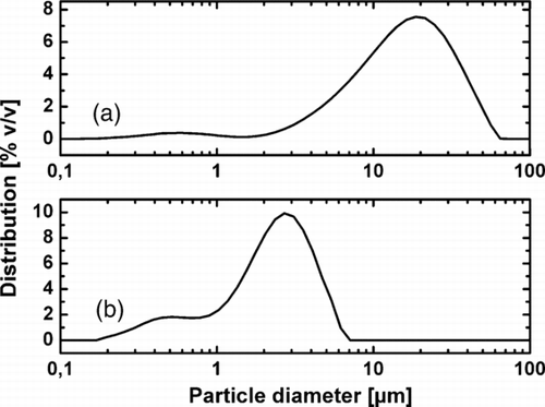
In , the particle size distributions of two different SAC particle fractions are shown, measured with a Malvern Mastersizer (Malvern Instruments Ltd.). Particle fraction (a) exhibits a wide distribution of larger SAC particles (named coarse fraction) with a mean diameter of 15.6 μm whereas in (b) a narrow distribution of small SAC particles with a mean diameter of 2.3 μm (named fine fraction) is shown. The density of the used SAC is 1,100 kg/m3.
FIG. 1 Particle distribution in volume percent (% v/v); (a) wide distribution of larger SAC particles with a mean diameter of 15.6 μm; (b) narrow distribution of small SAC particles with a mean diameter of 2.3 μm.
The charge to mass ratio (q/m value) of the SAC micro particles is dependent on their mean diameter. Measuring the q/m value (Nesterov et al. Citation2007), the fine particle fraction with a mean diameter of 2.3 μm yielded a ratio of up to –8.10–3 C/kg, in contrast to the coarse fraction with a mean diameter of 15.6 μm, possessing a charge to mass ratio of about –3.10–3 C/kg. This is partly explained by the fact that the surface to volume ratio is increased when the particle diameter is decreased. Due to the measurement technique, the obtained q/m value specifies only a mean charge value for the particle sample under consideration, thus, single particle charges can differ widely due to different microscopic charging processes (Charlson et al. Citation1992; Diaz Citation1997; Manouchehri et al. Citation2001).
Microelectronic Chip
A CMOS chip has been designed for defined spatial particle deposition (König et al. Citation2010). By addressing each pixel individually, any high voltage pattern can be programmed that attracts negatively charged micro particles, which will be deposited according to the pattern ().
FIG. 2 (top) CMOS chip with SAC particle deposition pattern with a total of 16,384 pixels on 1.28 × 1.28 cm2; (bottom) schematic deposition; two different kinds of particles are deposited on defined pixels consecutively.
Currently, the chip features 10,000 pixels per cm2 with a pixel pitch of 100 μm, resulting in a total of 16,384 pixels on 1.28 × 1.28 cm2.
The pixels have an aluminum surface and are surrounded, and thereby separated, by the grid electrode. The grid electrode and the pixels are located in the topmost metal layer of the chip and are isolated from each other by silicon dioxide. The grid is (in contrast to the pixels) covered by a silicon nitrite insulator to prevent electrical breakdown. In the experiments performed for this article, the voltages applied to each of the pixels were either 0 V or 100 V, the grid electrode was grounded or set to a constant voltage of 30 V. Further details will be discussed in the simulation section.
Aerosol Generation
To generate an aerosol, which can be brought into contact with the chip surface, an appropriate machine has been developed. A compact system consisting of several different particle containers, mounted on a vibrating plate to prevent undesired particle agglomeration, was designed. To generate reproducible aerosol quality with constant particle densities, the particles are siphoned out of their reservoir through an ejector by an air flow called transport air, as shown in .
FIG. 3 Principle of aerosol generation; particles are sucked out of a reservoir through an ejector, the aerosol is guided through a Teflon tube to the outlet, where the aerosol is brought into contact with the chip surface.
The density of the aerosol is controlled by an additional, separate air stream, called dosage air. This additional air stream forms a compound with the aerosol, rendered by the transport air, and thereby decreases the aerosol density. A Teflon tube connects each ejector with an outlet where the CMOS chip for peptide synthesis is brought into contact with the specific aerosol. A computer interface controls different electronic valves connected to pressurized air, in turn, the valves operate the air inlets discussed before. This ensures reproducible air flow durations.
To obtain triboelectrically charged micro particles, the particles are guided through a Teflon tube. Due to the turbulent flow in the tube, particles contact the inner surface of the tube, resulting in triboelectric charge of the particles.
Particle Deposition
The detailed geometry for the particle deposition is outlined in . The aerosol, generated as described in the last paragraph, enters the geometry through the aerosol inlet.
FIG. 4 Schematic geometry of aerosol outlet and CMOS chip position above the air stream for particle deposition.
Afterwards, particles and possible agglomerates have to pass a sieve with negative voltage of 1 kV. Due to the mesh size of about 25 μm, only particles with a smaller diameter can pass the sieve, agglomerates are held back or are destroyed, unable to reach the chip surface. The sieve voltage acts as a particle sorter, separating particles by charge: negatively charged particles, located between chip and sieve, are accelerated towards the chip; positively charged particles are decelerated and cannot reach the chip surface. Hence, positively charged particles are excluded from the aerosol stream at the sieve. The sieve therefore allows the selection of particles smaller than the mesh size and, furthermore, the selection of particles with equal charge signs. This reduces contaminations by restraining positively charged particles and particle agglomerations from entering the deposition region.
SIMULATION
Forces and Boundary Conditions
The process of particle deposition comprises various different forces interacting with the particles. We assume that particle movement does not influence the surrounding air flow and that particle-particle interaction (e.g., collision) is small due to a low aerosol density and can therefore be neglected. We also considered the gravitational force to be negligible for micro particles with a diameter of about 10 μm or less and a density similar to water.
We estimated the different electrical forces, considering a micro particle with a diameter of 10 μm and a charge per mass ratio q/m = –3.10–3 C/kg, located 50 μm beneath the chip surface. A simulation of the electrical field configuration for a typical voltage pattern on the chip revealed, that the dielectrophoretic force Fdep interacting with a particle, which features a dielectric constant of ϵ = 4, is Fdep≈ 7.9.10–14 N, being at least three orders of magnitude smaller than the electrical force Fel≈ 1.6.10–10 N. The image force, resulting from the particle charge interacting with the metallic chip surface in a distance of 50 μm can be calculated as Fimg= 2.3.10–12 N and is therefore also negligible.
Thus, we used two forces to describe the particle deposition on the CMOS chip: the electrostatic force F el and the drag force F drag. Hence, electrical and drag force add up to the total force F part, affecting a single particle:
The electrical force F el results from the gradient of the electrical potential U, due to applied voltages on charged surfaces, in our case the chip and the sieve:
For an accurate air flow simulation, the specific geometry () has to be taken into account. The initial aerosol stream velocity at the inlet is 1 m/s, the sieve was not taken into consideration for air stream deceleration, because the experimentally determined aerosol velocity was measured after passing the sieve. We assume that local air turbulences at the sieve, due to the small mesh size, can be neglected, as the distance between chip and sieve is much larger than the mesh size.
The following simulations for particle deposition analysis were obtained with the commercially available program COMSOL Multiphysics (COMSOL, Inc., USA), a finite element analysis solver, and simulation software. First, the stationary Navier-Stokes equation for the incompressible airflow was solved: The geometry shown in was discretized by means of Lagrange finite elements with an average area ratio of 2.6.10–5 each compared to the total area. This fine triangulation guarantees a good numerical solution to the incompressible Navier-Stokes equation, which was linearized and solved up to a relative uncertainty of 10–6 by the standard solver for stationary, non-linear differential equations. Second, the Poisson equation for the electrical field on the chip surface was solved on the same triangulation up to a relative uncertainty of 10–6 using the standard solver for electrostatic problems. Finally, particle trajectories were simulated, established on the solutions for the air velocity field and the electrical field in our geometry. The relative error tolerance of the solver basing on the Runge-Kutta methods of order four and five was also set to 10–6.
In the air velocity field is shown. The boundaries were assumed to exhibit the no slip condition, the inlet air velocity was 1 m/s, and the outlets were both set to comprise a pressure of 105 Pa. The density and the dynamic viscosity of the fluid were set to the coefficients ρair= 1.293 kg/m3 and ηair= 17.1 μPa s. In , the simulated electrostatic potential is shown for the geometry outlined in . All boundaries, except for the chip and the sieve, were assumed to have no charge.
FIG. 5 Simulation for the specific geometry as shown in ; (a) air velocity field; (b) electrostatic potential.
Deposition Concept
Particles, passing the sieve, enter the deposition region where the electrical fields between chip and sieve selectively guide the aerosol particles to the active deposition areas. Comparing the desired deposition pattern in (left) with the one obtained in a deposition experiment (, right), contaminations can be observed, indicating that the deposition conditions in practice still have to be improved. We experimentally verified that the more pixels are switched off in a voltage pattern on the chip surface, the more contaminations on these pixels can be observed after deposition.
FIG. 6 Desired particle deposition pattern (a, left) and experimentally achieved pattern (a, right); (b) schematic of particle deposition on a chip; particles move towards the chip and are manipulated by electrical fields resulting from the voltage pattern on the chip surface to enable spatial defined particle deposition.
To investigate the causes of contamination, a two-dimensional simulation model has been designed, as detailed in Figure 6b: particles with a predefined size and negative charge are attracted by the electrical field of the chip. The latter is modeled by two active pixels set at 100 V separated by three inactive pixels at 0 V each. Taking into account that the average particle diameter is about 5–10% of the size of one pixel, nine pixels are a sufficient chip detail to investigate the effects observed in experiments: Therefore, the entire chip does not have to be modeled for the simulation. Motivated by experiments, another pattern was modeled which consisted of two active pixels separated by seven inactive pixels as this combination showed a high probability of contamination.
Particles were injected into the air stream (Figures and ) in a distance of ∼1 cm away from the chip surface (near the sieve) with an initial particle and air stream velocity of v 0= 1 m/s in chip direction. Larger initial velocities up to 5 m/s were also simulated, but, the velocity variation in this range does not lead to a significant change in particle deposition and is therefore not considered in this article. The exponential decrease of electrical field intensity emanating from the chip thereby confines the region of interest, where the selective effect of the chip dominates particle manipulation. Simulations showed that this region extends only 200 μm from the chip surface, as we subsequently demonstrate.
In the simulations, we systematically varied the charge per mass ratio (q/m value) of the particles and the particle diameter. The sieve voltage was set to –1 kV, high enough to have an abundant selective effect on particles, and low enough not to risk destroying the chip by electrical breakdown and arc-over between sieve and chip. Pixel voltages on the chip were set to 100 V, the technical limit of the microchip used, and 0 V to obtain the greatest possible selective effect. The voltage of the grid electrode was set to 0 V () or 30 V ().
FIG. 7 Simulation detail of particle deposition on a chip; particles are 10 μm in diameter and feature a q/m value of –3.10–3 C/kg; (a) the voltage of the grid electrode is 0 V, several particles are deposited as contaminations on deactivated pixels; (b) voltage of the grid electrode is 30 V, excess particles are solely deposited on the grid electrode.
The effect of the grid electrode on particle deposition is illustrated in . Particle trajectories are represented as black lines; the electrical potential in V is shown in grey scale. Above the trajectories, the voltage pattern on the chip surface is indicated: Two pixels are switched to high voltage, in between 7 grounded pixels are located.
Particles with a diameter of 10 μm and a q/m value of –3.10–3 C/kg are deposited on the chip. In the grid electrode is grounded, just like the switched off pixels. Excess particles will reach the chip surface and will be deposited not only on the grid electrode, but also on the grounded pixels, causing contaminations. In comparison to this, shows the same particle deposition with the grid electrode set to 30 V. Particles, which are not deposited on the desired pixels, are solely deposited on the grid electrode. This allows using the grid electrode as an adsorber for excess particles, as long as not too many particles are deposited on the grid electrode. Thus, the described effect of the grid electrode is important for contamination free particle deposition. In all further simulations, the grid electrode is switched to 30 V.
Effect of the Particle Diameter on Deposition
In the simulation shown in , the particle size was altered between 3 and 10 μm ((a) 3 μm; (b) 5 μm; (c) 10 μm) and the charge per mass ratio (q/m value) of the particles was defined as –3.10–3 C/kg in all three cases.
FIG. 8 Simulation of particle deposition on a chip; particle trajectories are represented as black lines, grayscale represents the electrical potential [V]; particle diameters are (a) 3 μm, (b) 5 μm, (c) 10 μm; with q/m value of –3.10–3 C/kg; in all cases no contamination on grounded pixels occurs.
![FIG. 8 Simulation of particle deposition on a chip; particle trajectories are represented as black lines, grayscale represents the electrical potential [V]; particle diameters are (a) 3 μm, (b) 5 μm, (c) 10 μm; with q/m value of –3.10–3 C/kg; in all cases no contamination on grounded pixels occurs.](/cms/asset/95b0ceac-915e-436f-9fc2-37f08715b624/uast_a_517814_o_f0008g.gif)
The particle deposition in features very few deposition events on the chip surface. In and c, the number of deposition events rises with particle diameter. In this simulation, all particles are deposited either on the 100 V pixels or on the grid electrode, which resembles the ideal and desired deposition pattern.
In contrast to this simulation, experiments exhibit a crucial difference: Particles with a mean diameter of 10 μm or greater tend to be deposited on both active and grounded pixels and hence cause contaminations.
Now, the q/m value was altered in one order of magnitude. In , a value of –3.10–2 C/kg was used. In Figures and we simulated the same number of starting particles, but the overall number of deposition events on the chip surface has risen. In and b the particle deposition is still as desired, without contamination. In many particle trajectories end on grounded pixels, indicating contamination. Some trajectories near the 100 V pixels are incorrect due to the lack of adhesion forces, making odd bends near the chip surface.
FIG. 9 Simulation of particle deposition on a chip; particle trajectories are represented as black lines, grayscale represents the electrical potential [V]; particle diameters are (a) 3 μm, (b) 5 μm, (c) 10 μm; with q/m value of –3.10–2 C/kg; in (a, b) no contamination on grounded pixels occurs in contrast to (c).
![FIG. 9 Simulation of particle deposition on a chip; particle trajectories are represented as black lines, grayscale represents the electrical potential [V]; particle diameters are (a) 3 μm, (b) 5 μm, (c) 10 μm; with q/m value of –3.10–2 C/kg; in (a, b) no contamination on grounded pixels occurs in contrast to (c).](/cms/asset/d4fb4844-de13-4544-a609-1a7509d03213/uast_a_517814_o_f0009g.gif)
Intuitively, one would expect, that particles with a higher q/m value are easier to manipulate by electrical fields and therefore should yield a better deposition quality. However, this is not the case in the given configuration. A higher q/m value combined with a larger inert mass will cause particles to divert from their appointed path, determined by the electrical field configuration. A similar effect was also observed by Lee et al. (Citation2009). Due to the electrical potential between chip and sieve, particles with a higher charge are accelerated more intensely towards the chip. Hence, the efficiency of the selective local fields of the chip declines and the deposition quality decreases. Moreover, this also entails, that more particles will reach the chip surface, visible in the simulations as a higher overall number of deposition events.
These results imply that highly charged particles are an intrinsic characteristic of the aerosol created in our experiments. As stated in Nesterov et al. (Citation2010), highly triboelectrically charged particles with a surface charge density two orders higher than the critical surface charge density in air were observed. This seemingly paradox value was documented to be a common result for particles (Bailey Citation1993; Harper 1967). In fact, the critical surface charge density, defined as the value where electrical breakdown between two parallel metal plates occurs, is invalid for dielectric particles. Due to the curvature of a particle surface and their dielectric character, higher electrical surface fields are possible without electrical breakdown, allowing microscopic particles to maintain higher charges than macroscopically planar metal surfaces.
Concluding, a greater particle diameter yields higher particle inertia. On the other side, bigger particles possess a higher total charge. This leads to the result that a larger particle diameter causes contaminations in this case of spatial defined particle deposition by means of an aerosol.
Stopping Distance
The influence of the particle diameter on contamination may also be qualitatively demonstrated by a different approach: the stopping distance S of a particle, which is defined as the product of initial particle velocity v0 and the relaxation time τ of a particle, which in turn is the time needed, until a particle with no initial velocity, released into a moving fluid, reaches (1–1/e) ≈
63.2% of its final velocity vf. Hence, the relaxation time is defined as (Hinds 1999):
TABLE 1 Stopping distance S for different particle diameters d with corresponding Knudsen number Kn and Cunningham correction factor Cc; initial velocity is v = 1m/s
Due to the short stopping distance of smaller particles, these particles are easier to manipulate by electrical fields, resulting in highly precise particle deposition as shown in the simulations (Figures and b and and b).
Long-Range Electrical Fields
Another interesting effect, connected with the sieve voltage, is delineated in . Grayscale represents the electrostatic potential between the chip surface and the sieve. Particle trajectories are shown starting at the sieve and ending at the outlets or on the chip surface. In simulations, we started with 80 particles with a diameter of 10 μm; the q/m value was set to –3.10–3 C/kg. In , 17 out of 80 particles are deposited on the chip, the remaining particles move past the chip without being deposited and leave the deposition region through one of the outlets. In , the voltage of the sieve was set to 0 V instead of –1 kV. In this case, all 80 particles, except for one, move past the chip without being deposited. Only one single trajectory ends on the chip surface. The significant discrepancy in the number of deposited particles evolves in (a) due to the attracting force in chip direction, generated by the electrostatic potential between chip and sieve and in (b) due to the non-existing force, because the sieve is grounded.
FIG. 10 Simulation of particle deposition on a chip; the electrostatic potential [V] is shown in grayscale, particle trajectories are shown as black lines; particles are 10 μm in diameter and possess a q/m value of –3.10–3 C/kg; (a) the voltage of the sieve is –1 kV, several particle trajectories end on the chip surface; (b) the voltage of the sieve is 0 V, only one single particle trajectory ends on the chip surface; (c) schematic of a particle in the electrical field resulting from the charge of the aerosol and the chip surface, acting as opposing electrodes.
![FIG. 10 Simulation of particle deposition on a chip; the electrostatic potential [V] is shown in grayscale, particle trajectories are shown as black lines; particles are 10 μm in diameter and possess a q/m value of –3.10–3 C/kg; (a) the voltage of the sieve is –1 kV, several particle trajectories end on the chip surface; (b) the voltage of the sieve is 0 V, only one single particle trajectory ends on the chip surface; (c) schematic of a particle in the electrical field resulting from the charge of the aerosol and the chip surface, acting as opposing electrodes.](/cms/asset/055fd26f-54f9-4fed-99c3-103211d8e709/uast_a_517814_o_f0010g.gif)
This effect can also be observed when the number of particles in the simulation is increased by a factor of 10: Beginning with 800 instead of 80 particles, the simulation with no sieve voltage yielded only 7 deposited particles, whereas in the simulation with activated sieve voltage, 178 particles were deposited on the chip.
The experiment, in comparison, offers a completely different picture: Applying no voltage to the sieve, a lot of particles are deposited on the chip surface, which could not even be reproduced in simulations by altering the q/m value of the particles.
We suppose that the charged aerosol particles in the experiment have an effect similar to the sieve with a voltage of –1 kV on particles, located between the outlet and the chip. In therefore, the total charge of a particle cloud acts as a negative electrode. If we assume a uniform distribution of 0.1 mg of particles with 10 μm in diameter (∼1.7.105 particles) and a q/m value of –3.10–3 C/kg over a surface area of 1 cm2, we can substitute the sieve voltage in the simulation with a constant area charge density of δ= –2.7.10–6 C/m2, representing the charge of 0.1 mg particles. This resulted in an electrostatic potential of about –2 kV in proximity of this simulated particle layer, which then yielded the effects obtained in experiments, explaining the discrepancy between simulation and practical observations.
Thus, the sieve and the applied voltage provide an important tool in particle manipulation, due to long-range electrical fields comparable to a particle cloud. Additionally, the sieve provides us with the possibility to sustain reproducible and constant electrical fields.
Field Superposition
Another noticeable result using the fine particle fraction is shown in . We simulated particles with a diameter of 5 μm and a q/m value of –3.10–3 C/kg.
FIG. 11 Simulation of particle deposition on a chip; the electrostatic potential [V] is shown in grey scale, particle trajectories are shown as black lines; particles are 5 μm in diameter and possess a q/m value of –3.10–3 C/kg; (a) one pixel with 100 V is neighbored by 0 V pixels; particles tend to be deposited on the middle of the 100 V pixel; (b) three adjacent pixels with 100 V are neighbored by 0 V pixels; particles are deposited equally distributed on the 100 V pixel in the center, particles deposited on the left and right 100 V pixel tend to be deposited on the side of the pixel, into direction of the center pixel.
![FIG. 11 Simulation of particle deposition on a chip; the electrostatic potential [V] is shown in grey scale, particle trajectories are shown as black lines; particles are 5 μm in diameter and possess a q/m value of –3.10–3 C/kg; (a) one pixel with 100 V is neighbored by 0 V pixels; particles tend to be deposited on the middle of the 100 V pixel; (b) three adjacent pixels with 100 V are neighbored by 0 V pixels; particles are deposited equally distributed on the 100 V pixel in the center, particles deposited on the left and right 100 V pixel tend to be deposited on the side of the pixel, into direction of the center pixel.](/cms/asset/61c04954-ef55-4a12-acc3-81f55771ffc8/uast_a_517814_o_f0011g.gif)
The electrical charge pattern on the chip () comprised one single 100 V pixel. Here, particles tend to be deposited only at the center of the active pixel. In a similar effect was observed with three adjacent 100 V pixels, neighbored by 0 V pixels. In this case, particles are uniformly deposited on the central 100 V pixel, while the active pixels to the left and right of the central one are only half covered at the side adjacent to the central pixel. This simulated effect coincides with observations in experiments () and can be explained by the superposition of electrical fields. When attracting and repelling fields of direct adjacent 0 V and 100 V pixels unite, electrical fields are altered, such that particles will be deposited as observed in Figures and .
While the effect in is still acceptable for particle deposition, the result shown in is insufficient for combinatorial peptide syntheses.
EXPERIMENTAL RESULTS
As shown in the preceding sections, the simulations revealed that the particle size in combination with its maximum charge is a decisive parameter for spatially selective particle deposition. Focusing on this parameter, we optimized the particle production according to the simulations: The particle size distributions for two different particle fractions are shown in . The fine particle fraction is a result of the aforementioned optimization process. As discussed above, the fine particle fraction exhibits a narrow size distribution with a small mean diameter and, more importantly, a small maximum diameter of about 7 μm. The coarse particle fraction, in turn, has a wider size distribution with a larger mean and maximum diameter.
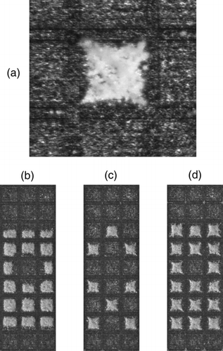
Using this fine particle fraction, a powerful improvement in particle deposition quality can be achieved, as shown in . In the particle deposition shows a high degree of contamination, although the checkerboard pattern in the lower left part of the picture is clearly visible with an almost acceptable grade of contamination. The mean diameter of particles used in this experiment was 15.6 μm. On the contrary, in , the deposition pattern is almost free of contamination, because theoretically achieved results were taken into account. The mean particle diameter here was 2.3 μm.
FIG. 12 Four different deposition patterns of micro particles on each chip surface (checkerboard, 1 of 16, 1 of 36, 1 of 64). (a) high degree of contamination; particles with a wide size distribution and a mean diameter of 15.6 μm were used; (b) almost free of contamination; particles with a narrow size distribution and a mean diameter of 2.3 μm were used.
Hence, after reproducing experimental results in simulations, the latter could, in turn, be verified by experiments, obtaining highly improved deposition results with the fine particle fraction. Furthermore, in , the grid electrode, in regions with a high proportion of 0 V pixels is covered with particles, whereas in the region of the checkerboard pattern, no particles are deposited on the grid.
As considered theoretically in , this function of the grid electrode is very important for contamination free deposition, because excess particles will always be part of particle deposition by means of an aerosol. Therefore an adsorber for these excess particles was inevitable in our experiments.
With the grid electrode set to 30 V, experiments showed that at least twenty consecutive particle depositions are possible without overloading the grid electrode with particles, which could yield notable contaminations. Due to the width of the grid electrode of only 15 μm, it is also important to use smaller particles. As shown in Figures and , smaller particles provide a lesser total number of deposition events on the grid, thus, avoiding particle overload.
The effect we described in the simulations shown in is omnipresent in experiments. In , particles with a mean diameter of 2.3 μm were deposited on a chip surface. In , a magnification of a particle deposition pattern with one single 100 V pixel surrounded by grounded pixels is shown. The deposition shows the typical experimentally observed characteristics: The pixel is entirely covered with particles, except for the borders. The corners however, are covered, because the gradient of the electrostatic potential is higher there compared to the edges. As the shape resembles a cushion pinned at the edges, we named this effect the pincushion-effect. Although particles were only deposited on charged pixels in , some pixels are only half covered or particles are only deposited in the center of the pixel. This effect can be explained by the superposition of electrical fields, resulting in the depicted deposition pattern.
FIG. 13 Deposition on a chip (mean particle diameter 2.3 μm) exhibiting the effect described in the simulations in ; (a) single pixel with the pincushion effect visible; (b) in dependence of the voltage of directly surrounding pixels, particles either tend to be deposited in the center or on the side of the pixel; to guarantee isotropic central coverage of pixels, the same deposition pattern is produced by two consecutive deposition steps (c) and (d).
The effect in Figures and is still acceptable for spatially defined particle deposition because the center of the pixel is covered isotropically. In contrast to this, the effect shown in Figures and impedes reliable particle deposition, as we require a reproducible deposition with homogeneous central coverage on each pixel. Being an intrinsic characteristic of the setup, as the simulations revealed, the effect only occurs when using smaller particle fractions, because of their precise deposition according to the electrical fields. Bigger particles hide this effect due to their less accurate deposition behavior. In order to circumvent this in experiments, one possibility is to divide the deposition pattern into several sub-patterns, such that directly adjacent 100 V pixels are not simultaneously active in one pattern. For instance, an area with all pixels to be covered can be produced by two consecutive deposition steps with two complementary checkerboard patterns ( and d). The disadvantage of this method is the increased number of necessary deposition steps. However, as simulations and experiments show, this guarantees isotropic central coverage while being simple to implement.
CONCLUSION
The objective of this article was to investigate the dynamics and the precise deposition of charged polymer micro particles onto a microelectronic chip. We engaged this task with a series of simulations, analyzing micro particle dynamics and deposition patterns on the chip. First, an analytical model is defined which is based on the drag force and the electrical force acting on the particles in the aerosol. The particle dynamics and flow in the presence of these fields is then investigated in simulations implemented in COMSOL, which numerically evaluates the equations of motion and calculates the particle trajectories by means of a finite element method.
Conducting simulations, we studied the influence of particle diameter, q/m value, long-range fields, and field superposition on the selective particle deposition process. The importance of the grid electrode as an adsorber for excess particles and thus preventing contaminations could be theoretically affirmed.
Concluding from the simulations, aerosols feature a wide charge distribution, especially particles with a high charge and a larger diameter will lead to contaminations. The results obtained led to experimental optimization in particle production. Using particles with a small mean (2–3 μm) and maximum diameter (<7 μm) reproducibly yields deposition patterns with very high precision. This can be explained by the lower inertia of small-sized particles which are therefore easier to manipulate by electrical fields.
Additionally, long-range fields of particle clouds significantly influence the deposition. A constant long-range electrical field can be generated by applying high voltage to a metallic sieve located parallel to the chip surface. Thus, the sieve provides an important tool in particle manipulation.
The experimentally observed pincushion-effect could be simulated, which restricts particle deposition to certain areas of a pixel in dependence of the surrounding voltage pattern applied to the chip. The simplest way to guarantee isotropic central pixel coverage is to divide a deposition pattern into two complementary checkerboard patterns, applied in consecutive deposition steps.
The simulated deposition patterns are in good compliance with the experiments. Investigating this, one should keep in mind that the results of the simulations also have their limits concerning the lowest bound of the particle diameter, as for particles smaller than 1 μm, molecular effects like Brownian motion become relevant. The latter then cause deviations from the equations of motion as currently simulated so that nano particles cannot be modeled using the COMSOL implementation presented here.
In contrast to this, a viable improvement of the current simulation implementation could be to include the interaction of particles with the particle cloud by adding the respective mean field term to the electrical field over the chip surface, which will be considered in further research together with the characteristics of the aerosol as, for instance, the aerosol density.
In the next step, the simulations presented here will also offer the possibility for theoretical miniaturization tests. As a reduction of the maximum pixel voltage to 60 or even 30 V allows for downscaled microelectronic components: the pixel pitch could be decreased to less than 65 μm (60 V) or 50 μm (30 V), which enables depositions on chips with pixel densities of over 40,000 spots/cm2.
The experimental results showed that particle patterning with this technique has the potential to become a powerful method for combinatorial chemistry applications. Additionally, this deposition technique might give rise to applications in large-area micro structuring of new materials.
Acknowledgments
The authors would like to thank V. Stadler, T. Felgenhauer, and K. Leibe for helpful discussions and D. Rambow, S. Heß, and J. Kretschmer for technical assistance. The aerosol generator was built in cooperation with the company R.O.T GmbH (Germany). The financial support by the Baden-Württemberg Stiftung is gratefully acknowledged.
REFERENCES
- Bailey , A. G. 1993 . Charging of Solids and Powders . J. Electrostatics , 30 : 167 – 180 .
- Beyer , M. , Nesterov , A. , Block , I. , König , K. , Felgenhauer , T. , Fernandez , S. , Leibe , K. , Torralba , G. , Hausmann , M. , Trunk , U. , Lindenstruth , V. , Bischoff , F. R. , Stadler , V. and Breitling , F. 2007 . Combinatorial Synthesis of Peptide Arrays onto a Microchip . Science , 318 : 1888
- Coulson , J. M. and Richardson , J. F. 1999 . “ Motion of Particles in a Fluid, in Particle Technology and Separation Processes. Ch. 3. ” . In Chemical Engineering, vol. 2 , Oxford : Butterworth-Heinemann .
- Charlson , E. M. , Charlson , E. J. , Burkett , S. and Yasuda , H. K. 1992 . Study of the Electrification of Polymers using Contact and Separation Current . IEEE T. Electr. Insul. , 26 : 1144 – 51 .
- Diaz , A. F. 1997 . Contact Electrification of Materials: The Chemistry of Ions on Polymer Surfaces . J. Adhesion , 67 : 111 – 122 .
- Fudouzi , H. , Kobayashi , M. and Shinya , N. 2002 . Site-Controlled Deposition of Microsized Particles Using an Electrostatic Assembly . Adv. Mater. , 14 : 1649 – 1652 .
- Harper , W. R. 1967 . Contact and Frictional Electrification , 13 – 21 . Oxford : Oxford University .
- Hinds , W. C. 1999 . Aerosol Technology. , New York : Wiley Interscience .
- Jacobs , H. O. and Whitesides , G. M. 2001 . Submicrometer Patterning of Charge in Thin-Film Electrets . Science , 291 : 1763
- Kim , H. , Kim , J. , Yang , H. , Suh , J. , Kim , T. , Han , B. , Kim , S. , Kim , D. S. , Pikhitsa , P. V. and Choi , M. 2006 . Parallel Patterning of Nanoparticles via Electrodynamic Focusing of Charged Aerosols . Nat. Nanotechnol. , 1 : 117 – 121 .
- Krinke , T. J. , Fissan , H. , Deppert , K. , Magnusson , M. H. and Samuelson , L. 2001 . Positioning of Nanometer-Sized Particles on Flat Surfaces by Direct Deposition from the Gas Phase . Appl. Phys. Lett. , 78 : 3708
- Krinke , T. J. , Deppert , K. , Magnusson , M. H. , Schmidt , F. and Fissan , H. 2002 . Microscopic Aspects of the Deposition of Nanoparticles from the Gas Phase . J. Aerosol. Sci. , 33 : 1341 – 1359 .
- König , K. , Block , I. , Nesterov , A. , Torralba , G. , Fernandez , S. , Felgenhauer , T. , Leibe , K. , Schirwitz , C. , Löffler , F. , Painke , F. , Wagner , J. , Trunk , U. , Bischoff , F. R. , Breitling , F. , Stadler , V. , Hausmann , M. and Lindenstruth , V. 2010 . Programmable High Voltage CMOS Chips for Particle-Based High-Density Combinatorial Peptide Synthesis . Sens. Act. B. , 147 : 418 – 427 .
- Lee , H. , You , S. , Gyu Woo , C. , Lim , K. , Jun , K. and Choi , M. 2009 . Focused Patterning of Nanoparticles by Controlling Electric Field Induced Particle Motion . Appl. Phys. Lett. , 94 : 053104
- Manouchehri , H. R. , Hanumantha Rao , K. and Forssberg , K. S. E. 2001 . Triboelectric Charge Characteristics and Donor-Acceptor, Acid-Base Properties of Minerals . Particul. Sci. Technol. , 19 : 23 – 43 .
- Nesterov , A. , Löffler , F. , König , K. , Trunk , U. , Leibe , K. , Felgenhauer , T. , Bischoff , F. R. , Breitling , F. , Lindenstruth , V. , Stadler , V. and Hausmann , M. 2007 . Measurement of Triboelectric Charging of Moving Micro Particles by Means of an Inductive Cylindrical Probe . J. of Phys. D Appl. Phys. , 40 : 6115 – 6120 .
- Nesterov , A. , Löffler , F. , Cheng , Y.-C. , Torralba , G. , König , K. , Hausmann , M. , Lindenstruth , V. , Stadler , V. , Bischoff , F. R. and Breitling , F. 2010 . Characterization of Triboelectrically Charged Particles Deposited on Dielectric Surfaces . J. Phys. D Appl. Phys. , 43 : 165301
- Pai , D. M. and Sprigett , B. E. 1993 . Physics of Electrophotography . Rev. Mod. Phys. , 65 : 163 – 211 .