Abstract
We report production of bimetallic nanostructured copper– silver coatings by in situ deposition and sintering of metal nanoparticles produced as an aerosol. The metal nanoparticles themselves have potential applications in printed electronics, catalysis, antibacterial coatings, and heat transfer fluids. In many applications, nanoparticles are dispersed in an ink, which is then printed or coated onto a substrate and converted into a nanostructured thin film. Direct deposition from the aerosol allows us to produce nanostructured thin films without first dispersing the particles in a solvent. The high temperature reducing jet process allows formation of these metal nanoparticles from low-cost metal salt precursors in the gas phase. In this method, a fuel-rich hydrogen flame provides a low-cost source of energy to drive nanoparticle formation in a reducing environment. The aqueous precursor solution is delivered into the hot combustion product gases within a converging–diverging nozzle. The high-speed gas flow atomizes the precursor and provides exceptionally rapid mixing of the precursor with the hot gases. Here, particles are formed, then immediately quenched and deposited on a glass substrate. The effect of the silver content of the mixed copper–silver films on their electrical conductivity was studied systematically, revealing an abrupt transition from low conductivity to high conductivity between 30 wt.% and 40 wt.% silver.
Copyright 2013 American Association for Aerosol Research
1. INTRODUCTION
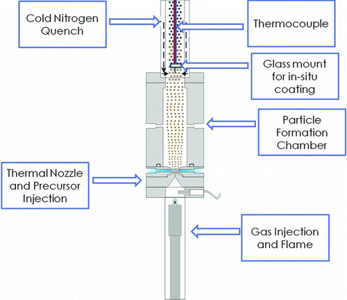
The synthesis of metallic nanoparticles is of great current interest and potential future industrial importance. Compared to the corresponding bulk materials, nanoparticles may have improved catalytic, optical, and electronic properties due to their high surface to volume ratio, confinement of free electrons within finite domains, and changes in their electronic structure at very small sizes. Applications of metal nanoparticles include inks for printed electronics and radio frequency identification (RFID) technology, antibacterial and conductive coatings, and enhancement of thermal conductivity of process fluids (Lee et al. Citation2008; Grouchko et al. Citation2009). These properties depend upon the size, shape, and composition of the metal nanoparticles. Recent advances include synthesis of hybrid structures such as bimetallic nanoparticles and alloys. Interesting properties can arise in bimetallic structures through synergistic effects of their components (Baber et al. Citation2010; Calderone et al. Citation2011; Wang et al. Citation2011). Bimetallic alloys such as Cu–Pd and Ag–Pd have been used as electrocatalysts for the oxygen reduction reaction and for hydrogen purification (Piper Citation1966; Milhano and Pletcher Citation2008; Tang et al. Citation2011). Single component nanoparticles (e.g., Ag, Pt, and Au) have been widely studied, but much room remains for exploring interesting properties of multicomponent and alloy nanoparticles (Grouchko et al. Citation2009). Silver nanoparticles have been widely used in conductive nanoink formulations as well as in RFID technology (Gamerith et al. Citation2007; Jung et al. Citation2007; Cheon et al. Citation2011). Silver is effective for use in conductive inks not only because metallic silver has high room temperature electrical conductivity (∼6 × 10⁷ S/m; Haynes Citation2011), but also because its oxide also has appreciable conductivity (of order 106 S/m). However, the relatively high cost of silver motivates a search for alternatives to it. Copper has electrical conductivity similar to that of silver (∼6 × 10⁷ S/m; Haynes Citation2011) and is much lower in cost than silver, but oxidizes rapidly in air. Due to their high surface area, copper nanoparticles oxidize quite rapidly to a mixture of cuprous oxide (Cu2O) and cupric oxide (CuO). These oxides of copper behave as undoped semiconductors. The electrical conductivity of Cu2O lies in the range of 10−2 to 10−1 S/m, while that of CuO is roughly 2 × 10⁻⁴ S/m (Haynes Citation2011). Previously, researchers have synthesized multicomponent nanoparticles using several methods, including colloidal synthesis in the presence of reducing and capping agents, microemulsion templated synthesis, and microwave-assisted synthesis (Grouchko et al. Citation2009; Blosi et al. Citation2010; Magno et al. Citation2010; Hsu et al. Citation2011). The colloidal synthesis approaches are effective in controlling the shape and size of nanoparticles. However, they are energy intensive, challenging to scale up, and often employ organic solvents with negative environmental impacts. Researchers have also tried to synthesize hybrid metal nanoparticles using spray pyrolysis. Many of the approaches to producing nanostructured alloys employ multistep synthesis procedures and incorporate post-synthesis treatment processes such as mechanical mixing of different powders, sintering, and mechanical compaction (Strobel et al. Citation2005; Athanassiou et al. Citation2010; Luechinger et al. Citation2010) for achieving alloying and/or nanoscale mixing. In the present work, we report the single step direct synthesis of bimetallic copper–silver nanostructured particles and films using the high temperature reducing jet (HTRJ) flame-based process. The objective of this work was to synthesize a bimetallic coating using copper and silver with minimal use of silver to lower the cost and to meet the desired industrial window of electrical conductivity (>100 S/m) for the aforementioned applications. The advantages of HTRJ technology stem from the use of low-cost, water-soluble nitrate precursors and a low-cost energy source in a continuous and environmentally benign process. The flame-based aerosol reactor configuration used to make these nanostructured coatings was developed by Scharmach et al. (Citation2010) and is described further below. The key addition to the previously described system was a holder for mounting a 12.5 mm diameter substrate in the aerosol flow, just above the particle formation chamber, as shown in . This allowed direct deposition of nanostructured films onto a glass substrate. These films were characterized for electrical conductivity vs. composition (fraction silver in silver/copper bimetallic films). In the bulk, copper and silver are nearly immiscible, and thus formation of separate copper and silver domains was anticipated. However, the morphology of the domains (separate Cu and Ag nanoparticles, core–shell particles, or more complex nonequilibrium structures) cannot readily be predicted.
FIG. 1 Schematic diagram of high temperature reducing jet (HTRJ) reactor. (Color figure available online.)
2. EXPERIMENTAL
2.1. Materials and Synthesis
Our prototype HTRJ reactor was described in detail by Scharmach et al. (Citation2010). It uses oxygen at a flow rate of ∼2.3 standard liters per minute (SLM) and a larger flow of hydrogen and nitrogen (∼14 SLM total) to form an inverted diffusion flame. Excess hydrogen is always used, so the flame temperature depends primarily on the oxygen flow rate. The hot combustion products are accelerated through a converging–diverging nozzle. The precursor is delivered within the nozzle by four small symmetrically arranged inlets. The high-velocity hot gas stream atomizes the precursor solution, which rapidly evaporates and decomposes, producing metal or metal oxide particles. Any oxides formed are reduced by the excess hydrogen present in the system. This reactor provides a general method of producing nanoparticles of metals that can be reduced by H2 in the presence of water.
Precursors used in these experiments included silver nitrate (ACS reagent, ≥99.0%, Acros Organics, Morris Plains, NJ, USA) and copper nitrate (ACS reagent, ≥98.0%, Acros Organics). For all experiments reported here, the precursor solution had a total metal concentration of 10 mM and was supplied at a flow rate of 180 ml/h. Nanoparticles were collected using a 293 mm diameter Durapore brand polyvinylidene difluoride membrane filter with 0.2 μm pore size. This provides efficient particle collection with minimal pressure drop at the flow rates used here. Nanostructured coatings were deposited on 12.5 mm diameter glass windows (Edmund Optics, Singapore). A single deposition substrate (window) was mounted perpendicular to the gas flow, on the reactor axis, just above the reactor exit. The substrate temperature was measured with a thermocouple touching the back side of the aluminum scanning electron microscopy (SEM) sample stub upon which the glass window was mounted. The measured temperature was typically ∼200°C.
2.2. Nanoparticle Characterization
The silver, copper, and silver–copper nanoparticles and coatings were analyzed by a series of methods: X-ray diffraction (XRD; Rigaku Ultima IV X-Ray Diffractometer, Rigaku, The Woodlands, TX, USA), transmission electron microscopy (TEM; JEOL JEM 2010 at an accelerating voltage of 200 KV; JEOL, Ltd., Tokyo, Japan), and SEM (AURIGA™ CrossBeam® Workstation (FIB-SEM) from Carl Zeiss SMT, Oberkochen, Germany) with an Oxford Instruments (Oxford Instruments, Scotts Valley, CA, USA) X-Max® 20 mm2 energy-dispersive X-ray spectrum (EDS) detector and INCA® (Oxford Instruments, Scotts Valley, CA, USA) software for elemental composition determination. A custom-built electrostatic sampler, similar to that described by Dixkens and Fissan (Citation1999), was used for collecting particles directly onto TEM grids for offline analysis. For bulk electrical conductivity of coatings, a four-point probe with a Keithley 2400 sourcemeter was used. An atomic force microscopy (AFM) with camera scan head (Nanosurf Easyscan 2) was used to image the copper–silver coatings and determine their thickness and root mean square roughness. A scanning mobility particle sizer (SMPS) consisting of an ultrafine condensation particle counter (UCPC, TSI Model 3776, TSI, Inc., Shoreview, MN, USA) coupled with a short differential mobility analyzer (DMA, TSI model 3085, TSI, Inc.), a high voltage power supply (Bertan Model 205 B- 10 R; Bertan, Hicksville, NY, USA), and home-built Po210 neutralizer was used to measure electrical mobility-based particle size distributions (PSDs). For this, a small fraction of the reactor effluent was diverted and diluted with cold nitrogen before entering the SMPS, while the majority of the flow still passed through the collection filter.
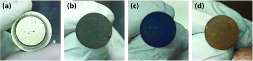
FIG. 2 Nanocoatings deposited on glass substrates in the HTRJ reactor from (a) silver only (100 wt.%); (b) copper (37.0 wt.%)–silver (63 wt.%); (c) copper (57.9 wt.%)–silver (42.1 wt.%); and (d) copper (70.2 wt.%)–silver (29.8 wt.%). (Color figure available online.)
3. RESULTS AND DISCUSSION
In the experiments described here, we produced pure silver, pure copper, and mixed copper–silver nanostructured films. These coatings were made by directly depositing nanoparticles onto the glass substrate during HTRJ nanoparticle synthesis from silver nitrate, copper nitrate, or mixed precursors. Silver nitrate is a low-cost silver salt that is highly soluble in water, sublimes above 212°C, and decomposes at 450°C to give silver oxides (Kirshenbaum et al. Citation1953; Patnaik Citation2001; Wang et al. Citation2009). Copper nitrate is also water soluble, and much lower in cost than silver nitrate, sublimes at 114°C, and decomposes at about 350°C (Ding et al. Citation2002). At the temperatures prevalent during synthesis, water is expected to rapidly evaporate from the mist of atomized liquid precursors leaving behind the solid silver and copper nitrates. These solid nitrates sublime and decompose into gaseous species from which nanoparticles nucleate. In the high temperature reducing atmosphere of the reactor, silver and copper oxides are reduced to metallic silver and copper. Experiments were designed in a systematic manner with coatings of pure silver synthesized first followed by deliberate addition of copper to evaluate its effect on the electrical conductivity. shows images of nanostructured coatings made with varying copper content, from zero (pure silver) to 70.2 wt.%.
shows the surface morphology of these coatings observed using SEM for the composition range shown in . shows that pure silver coatings had a morphology of nanoparticles that have partially coalesced to form larger islands. shows a film with 63 wt.% Ag and 37 wt.% Cu, which has excess silver domains presumably formed by coalescence of smaller silver particles. The size of each of these coalesced nanoparticles is around 100–150 nm. In the film shown in , with a composition of 57.9 wt.% Cu, 42.1 wt.% Ag, the distribution of Cu and Ag is much more uniform. In , one can see separated silver-rich and copper-rich domains in the coating that is made of 70.2 wt.% Cu, 29.8 wt.% Ag overall. Energy-dispersive X-ray spectroscopy confirmed that the brighter domains were copper-rich, while the dimmer domains were silver-rich.
FIG. 3 SEM images of nanoparticle coatings deposited on glass substrates in the HTRJ reactor from (a) silver only (100 wt.%); (b) copper (37.0 wt.%)–silver (63 wt.%); (c) copper (57.9 wt.%)–silver (42.1 wt.%); and (d) copper (70.2 wt.%)–silver (29.8 wt.%).
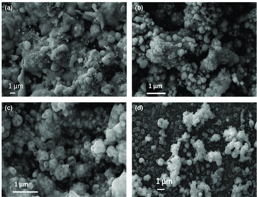
FIG. 4 Detailed characterization of copper–silver bimetallic coating deposited on a glass substrate from precursors with 42.1 wt.% Ag, 57.9 wt.% Cu: (a) SEM image taken at 35k× magnification; (b) FIB milled (2 nA for 150 s) top layer—showing many nanoparticles coalesced together; (c) FIB image showing view of coating at 36°. The entire coating was milled in the square region (2 nA for 180 s) where the glass substrate is visible; (d) TEM image of copper-silver mixed particles below 20 nm in diameter–inset electron diffraction pattern shows mainly the diffraction rings due to silver, but the Cu (111) plane is also visible; (e) HRTEM image of a single copper nanocrystal with a lattice spacing of d = 2.05 Å; (f) HRTEM image of a silver nanocrystal with a lattice spacing of d = 2.34 Å; (g) box average energy-dispersive X-ray spectrum (EDS) of copper–silver hybrid coating, indicating the presence of Cu and Ag. The silicon signal arises from the substrate. (h) Composition (in wt.% and at.%) as obtained from the EDS spectrum in part (g). (Color figure available online.)
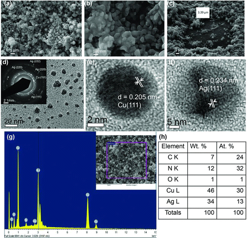
The mechanism of formation of metallic nanoparticles by reducing the oxides at elevated temperatures has been described by various research groups (Kirshenbaum et al. Citation1953; Ding et al. Citation2002; Wang et al. Citation2009). The size range of silver nanoparticles seen under TEM was less than 10 nm and copper nanoparticles were less than 50 nm. The larger size of the copper particles is attributed to the lower decomposition temperature of copper nitrate. As a result, copper nanoparticles nucleate earlier and have a longer time for growth. Thermal decomposition of silver nitrate is expected to take place via the following overall reaction steps:
A more accurate determination of thickness was carried out by AFM measurement in contact mode. For thickness measurement, the 58 wt.% Cu–42 wt.% Ag coating was chosen and the coating was scratched along the diameter of the substrate. The relative height difference between the bare substrate and coating was measured by scanning the probe tip perpendicular to the scratch. The thickness was calculated locally at various locations by drawing a horizontal line in a 50 × 50 μm2 square area and then averaged to give a thickness value of 1.25 μm. AFM measurement also yielded a root mean squared average (Rq ) roughness value of 450 nm. shows these AFM measurements for a 58 wt.% Cu–42 wt.% Ag coating. shows a two-dimensional top-view AFM micrograph used to measure the roughness locally in a 50 × 50 μm2 square area. shows a three-dimensional AFM micrograph to illustrate the nonuniform and rough nature of these nanostructured films, consistent with the SEM imaging.
FIG. 5 AFM characterization of copper–silver bimetallic coating deposited on a glass substrate from precursors with 42.1 wt.% Ag, 57.9 wt.% Cu; (a) two-dimensional AFM micrograph showing roughness measurement locally; (b) three-dimensional AFM micrograph showing the nonuniform and rough nature of the nanostructured film. (Color figure available online.)
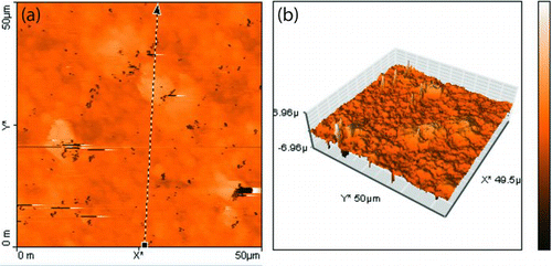
FIG. 6 Overlay of powder X-ray diffraction patterns of particles produced at various copper–silver precursor ratios: (a) 84.1 wt.% Cu–15.9 wt.% Ag; (b) 70.2 wt.% Cu–29.7 wt.% Ag; (c) 57.9 wt.% Cu–42.1 wt.% Ag; and (d) 37.1 wt.% Cu–62.9 wt.% Ag. The first inset shows a magnified view of the Ag (111) peak showing peak broadening and shift a toward the Cu (111) position with increasing copper content. The table inset shows the crystallite size obtained from application of the Scherrer equation to the Ag (111) peak in these spectra. (Color figure available online.)
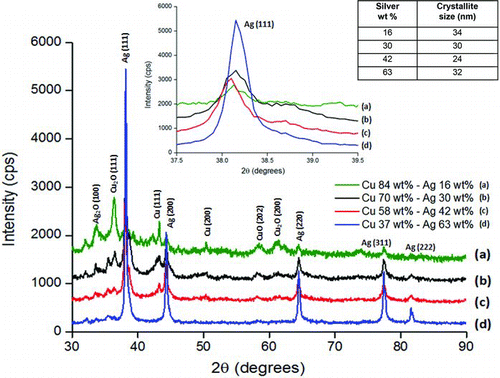
FIG. 7 Particle size distribution as measured using a scanning mobility particle sizer (SMPS) for pure silver, pure copper, and 57.9 wt.% Cu–42.1 wt.% Ag mixture. (Color figure available online.)
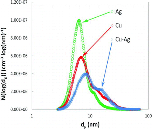
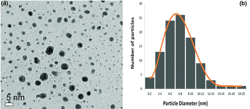
FIG. 8 Particle size distribution (PSD) from TEM imaging determined using Image-J software: (a) representative TEM image of pure silver nanoparticles collected directly onto TEM grid using the electrostatic precipitator; (b) PSD of pure silver nanoparticle synthesized at oxygen flow rate = 2.3 SLPM as determined from the TEM images like that shown in part (a). (Color figure available online.)
The mixed copper–silver particles were also analyzed by powder XRD in the scan range of 2θ = 30o–90o using Cu Kα X-rays. The overlaid XRD patterns of nanoparticles prepared at varied copper–silver ratios are shown in . For the silver-rich composition of 37.0 wt.% copper–63.0 wt.% silver (curve d), the diffraction of silver was dominant, but the silver peaks were broadened, indicating some degree of alloying with copper. Decreasing the silver content to 57.9 wt.% Cu–42.1 wt.% Ag (curve c) led to the appearance of distinct peaks corresponding to metallic copper and copper oxide phases. A degree of alloying is suggested by Ag (111) peak broadening and the merger of Ag (200) and Cu (111) peaks. When the silver content was decreased to 70.2 wt.% Cu–29.8 wt.% Ag (curve b), the copper and copper oxide peak intensities increased. Finally, spectrum (d) shows the pattern from particles produced from a precursor solution with 84.1 wt.% copper–15.9 wt.% silver (curve a). This copper-rich coating oxidized upon exposure to air, yielding a mixture of Cu, CuO, and Cu2O. The diffraction due to metallic silver was less prominent. Again, the Ag (111) peak position was slightly shifted toward the Cu (111) peak, indicating a degree of alloying. The Ag (111) peak is shown in magnified view in the inset of , which shows the shift toward the Cu (111) peak and peak broadening as the silver content of the precursor solution was increased. Crystallite size was calculated by applying Scherrer's equation to the Ag (111) reflection in the XRD spectra. Results are tabulated in an inset of . The crystallite size for the 57.9 wt.% Cu–42.1 wt.% Ag coating was the smallest, at 24 nm, but the variation in crystal size with composition was not dramatic. In all cases, the crystallite diameter measured in the films was substantially larger than the diameter of the particles formed in the gas phase, indicating substantial sintering and crystal growth even at the low deposition temperature near 200°C.
In the present study, all copper–silver coatings were synthesized at an oxygen flow rate of 2.3 SLPM (standard liters per minute), which was selected on the basis of previous optimization of the precursor atomization. To determine the PSD under these conditions, SMPS measurements were carried out during nanoparticle formation. Results from three different scans performed during the production of nanoparticles of varying composition at otherwise identical operating conditions are reported in . The geometric mean and geometric standard deviation of nanoparticles as determined from SMPS measurement were dg = 6.8 nm, σg = 1.4 for silver, dg = 8.5 nm, σg = 1.6 for copper, and dg = 9.8 nm, σg = 1.6 for the 58 wt.% copper–42 wt.% silver mixture. The PSD for 57.9 wt.% copper–42.1 wt.% silver composition was found to be broader and centered at slightly larger size compared to pure silver or pure copper under similar operating conditions. The PSD for pure silver nanoparticles calculated using TEM and particle imaging software is consistent with SMPS measurements. shows a representative TEM image of pure silver nanoparticles used for measuring PSD and shows the actual PSD for a count of 100 particles. The geometric mean particle size and geometric standard deviation calculated using Image-J software were found to be dg = 6.1 nm, σg = 1.7, which is in close agreement with SMPS results.
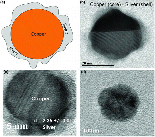
Copper–silver film formation on the glass substrate occurs via thermophoretic deposition of pure component, alloy, and or bi-component nanocrystals on the glass substrate, followed by diffusion that can lead to both particle sintering and growth and to copper–silver phase separation. At the low deposition temperatures used here (∼200°C), this may be dominated by surface diffusion on the high surface area particles, rather than bulk diffusion. HRTEM imaging provides insight into the particle morphologies obtained within the HTRJ reactor at the 58 wt.% Cu–42 wt.% Ag precursor ratio. shows an illustrative image of a core (copper)–shell (silver) nanocrystal. show HRTEM micrographs of copper (core)–silver (shell) particles observed by HRTEM, while shows a polycrystalline nanoparticle comprised of five crystallites. No single, dominant morphology was observed. Rather, a mix of such structures was obtained.
FIG. 9 HRTEM imaging of copper–silver bimetallic particles obtained from precursors with 42.1 wt.% Ag, 57.9 wt.% Cu: (a) illustrative image of core (copper)-shell (silver) particle; (b) core (copper)-shell (silver) morphology seen in high-resolution TEM micrograph; (c) another core (copper)-shell (silver) bimetallic particle with silver as shell, showing a lattice fringe spacing of 2.35 ± 0.01 Å; and (d) a polycrystalline nanoparticle of ∼10 nm size. (Color figure available online.)
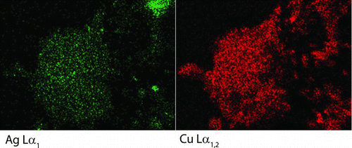
EDS measurements and EDS elemental mapping were also carried out on Cu–Ag nanopowders collected on filter paper, for various precursor compositions. A representative EDS result from nanopowder obtained from precursors with 42.1 wt.% Ag–57.9 wt.% Cu is shown in . The mass ratio of Ag/Cu in the nanopowder as measured by EDS analysis was found to be 0.74. The mass ratio of Ag/Cu in the precursor solution was 0.73, and that measured for the coating was 0.74. These are equal to within the uncertainty of the EDS measurements. EDS results from the nanopowder and the coating were in good agreement with each other, supporting the conclusion that the coating is formed by particle deposition and does not include a substantial contribution from chemical vapor deposition. The fact that the EDS results for both the nanopowder and coating matched the composition of Cu and Ag in the precursor solution demonstrates the ability of the HTRJ process to provide accurate control over composition and to fully convert precursors to products. This contrasts with typical chemical vapor deposition processes, in which different precursors react with different efficiencies, making composition control difficult and usually leading to incomplete precursor utilization. EDS mapping of copper and silver was done for the sample shown in , to assess the relative distribution of both elements in the nanopowder. The EDS maps in show that silver and copper are uniformly distributed in the nanopowder. The relatively higher intensity of copper compared to silver is due to the higher wt.% of copper in the precursor mixture and product powder.
FIG. 10 Energy-dispersive X-ray spectroscopy for a nanopowder obtained from precursors with 42.1 wt.% Ag–57.9 wt.% Cu. The inset image shows the region over which the box averaged EDS spectrum was captured. The inset table gives the elemental concentrations determined from EDS. The ratio of Ag/Cu = 0.74, which is identical to that measured in the coating. (Color figure available online.)
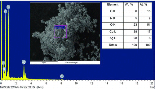
FIG. 11 EDS elemental maps of (a) copper and (b) silver for nanopowder obtained from precursors with 42.1 wt.% Ag–57.9 wt.% Cu, showing a uniform distribution of both elements in the nanopowder with higher relative intensity of copper than silver. (Color figure available online.)
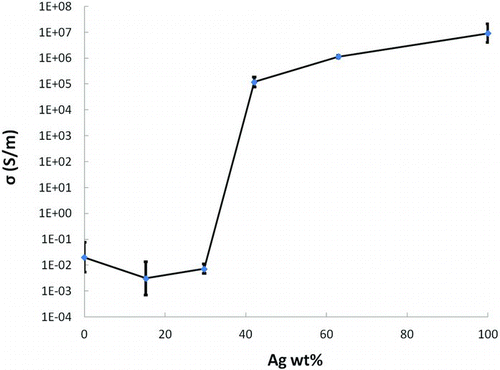
As described above, our aim was to obtain a high value of bulk electrical conductivity in these nanostructured films while minimizing the silver content. The copper–silver coating with 57.9 wt.% Cu–42.1 wt.% Ag was the lowest silver content that showed electrical conductivity comparable to bulk metals. The electrical conductivity vs. overall composition is shown in . The average conductivity values of nanostructured coatings are plotted against silver wt.%. The coatings with higher copper content had low conductivity, of the order of 10−2 to 10−3 S/m, which is similar to the conductivity expected for CuO or Cu2O (Young and Schwartz Citation1969; Patil et al. Citation1978; Kumar Barik et al. Citation2003). We attribute the abrupt decrease in conductivity below 42.1 wt.% Ag to oxidation of the copper component of the film and a resulting lack of conductive pathways through the film. The high electrical conductivity of the copper–silver nanocoatings with >40 wt.% silver is attributed to uniform mixing of copper and silver domains that allowed development of a percolation path for current through the film, along with a reduced degree of copper oxide formation due to mixing with silver. The adherence of the coatings was tested using the “scotch-tape” test and all the prepared coatings were found to be strongly adhered to the substrate. When the tape was peeled off, very few particles adhered to the tape, and the coatings remained intact. The adhesion of metal nanoparticles onto glass substrate is expected to be based upon purely physical adhesion arising from Van der Waals forces. The adhesion is strong simply because there is very good contact between the nanoparticulate film and the surface. The number of surface/particle contacts in a dense, nanoparticulate film is very high compared to a film deposited from larger particles. The nanoparticle deposition occurs due to thermophoresis driven by the large temperature gradient between the particle formation chamber (∼800°C) and substrate (∼200°C). This deposition mechanism is gentle—the particles are deposited with relatively low velocity and low kinetic energy. Particles in this nanometer size range are well known to sinter at low temperatures, and the SEM imaging presents clear evidence of substantial sintering to produce structures larger than the deposited particles (separately imaged in TEM). There may be some similar interdiffusion of metal into the glass substrate, but we have not seen any direct evidence of that.
FIG. 12 Electrical conductivity as a function of Ag wt.%. Error bars are plus or minus one standard deviation of log(σ). (Color figure available online.)
4. CONCLUSION
We demonstrated the synthesis of pure copper, pure silver, and copper–silver nanostructured coatings using the flame-based HTRJ reactor. The size of copper and silver nanoparticles prepared in this process was below 20 nm. Direct deposition of nanostructured coatings with in situ sintering at about 200°C allowed us to test the composition dependence of the conductivity without any intermediate processing steps such as ink formulation and spin coating or printing. Nanostructured coatings with at least 42 wt.% silver had metal-like conductivity high enough for all conductive thin film or printed electronic applications where silver-based inks are presently used. Displacement of silver by copper in such applications could result in substantial cost decreases. The promising copper–silver bimetallic coating was fully characterized by SEM, HRTEM, EDS, AFM, and FIB techniques showing that the 42.1 wt.% Ag, 57.9 wt.% Cu film contained well-mixed copper-rich and silver-rich nanodomains. The HTRJ flame-based process allows preparation of these mixed nanostructured films or nanopowders using low-cost, water-soluble metal salt precursors and could thereby provide a low-cost route to such materials.
Acknowledgments
This work was supported by the U.S. National Science Foundation (grant CBET-0652042). We thank Dr. Yueling Qin, University at Buffalo Integrated Nanostructured Systems Instrumentation Facility for help with TEM and FIB imaging.
REFERENCES
- Athanassiou , E. K. , Grass , R. N. and Stark , W. J. 2010 . Chemical Aerosol Engineering as a Novel Tool for Material Science: From Oxides to Salt and Metal Nanoparticles . Aerosol Sci. Technol. , 44 : 161 – 172 .
- Baber , A. E. , Tierney , H. L. and Sykes , E. C. H. 2010 . Atomic-Scale Geometry and Electronic Structure of Catalytically Important Pd/Au Alloys . ACS Nano. , 4 : 1637 – 1645 .
- Blosi , M. , Albonetti , S. , Gatti , F. , Dondi , M. , Migliori , A. Ortolani , L. 2010 . “ Au, Ag and Au-Ag Nanoparticles: Microwave-Assisted Synthesis in Water and Applications in Ceramic and Catalysis ” . In Nanotechnology 2010: Advanced Materials, CNTs, Particles, Films and Composites , 352 – 355 . Anaheim, CA , , USA : Nano Science and Technology Institute .
- Calderone , V. R. , Shiju , N. R. , Ferre , D. C. and Rothenberg , G. 2011 . Bimetallic Catalysts for the Fischer-Tropsch Reaction . Green Chem. , 13 : 1950 – 1959 .
- Cheon , J. M. , Lee , J. H. , Song , Y. and Kim , J. 2011 . Synthesis of Ag Nanoparticles using an Electrolysis Method and Application to Inkjet Printing . Colloid Surf. A: Physicochem. Eng. Asp. , 389 : 175 – 179 .
- Ding , Z. , Martens , W. and Frost , R. L. 2002 . Thermal Activation of Copper Nitrate . J. Mater. Sci. Lett. , 21 : 1415 – 1417 .
- Dixkens , J. and Fissan , H. 1999 . Development of an Electrostatic Precipitator for Off-Line Particle Analysis . Aerosol Sci. Technol. , 30 : 438 – 453 .
- Gamerith , S. , Klug , A. , Scheiber , H. , Scherf , U. , Moderegger , E. and List , E. J. W. 2007 . Direct ink-jet printing of Ag-Cu nanoparticle and Ag-precursor based electrodes for OFET applications . Adv. Funct. Mater. , 17 : 3111 – 3118 .
- Grouchko , M. , Kamyshny , A. and Magdassi , S. 2009 . Formation of Air-Stable Copper-Silver Core-Shell Nanoparticles for Inkjet Printing . J. Mater. Chem. , 19 : 3057 – 3062 .
- Haynes , W. M. 2011 . “ Electrical Resistivity of Pure Metals ” . In CRC Handbook of Chemistry and Physics , (92nd ed.) , 12 – 41 . Boca Raton , FL : CRC Press .
- Hsu , S.-W. , On , K. , Gao , B. and Tao , A. R. 2011 . Polyelectrolyte-Templated Synthesis of Bimetallic Nanoparticles . Langmuir , 27 : 8494 – 8499 .
- Jung , J.-K. , Choi , S.-H. , Jang , M. , Joung , J. and Joo , Y.-C. 2007 . Characteristic Microstructure Evolution of Polycrystalline Ag Films Prepared From Ink-Jetted Ag Nanoparticle Suspension . Mater. Sci. Forum. , 558–559 : 1243 – 1248 .
- Kirshenbaum , A. D. , Streng , A. G. and Hauptschein , M. 1953 . The Thermal Decomposition of Silver Salts of Perfluoro Carboxylic Acids . J. Amer. Chem. Soc. , 75 : 3141 – 3145 .
- Kumar Barik , U. , Srinivasan , S. , Nagendra , C. L. and Subrahmanyam , A. 2003 . Electrical and Optical Properties of Reactive DC Magnetron Sputtered Silver Oxide Thin Films: Role of Oxygen . Thin Solid Films , 429 : 129 – 134 .
- Lee , Y. , Choi , J.-R. , Lee , K. J. , Stott , N. E. and Kim , D. 2008 . Large-Scale Synthesis of Copper Nanoparticles by Chemically Controlled Reduction for Applications of Inkjet-Printed Electronics . Nanotechnology , 19 : 415604/415601 – 415604/415607 .
- Luechinger , N. A. , Grass , R. N. , Athanassiou , E. K. and Stark , W. J. 2010 . Bottom-Up Fabrication of Metal/Metal Nanocomposites from Nanoparticles of Immiscible Metals . Chem. Mater. , 22 : 155 – 160 .
- Magno , L. M. , Sigle , W. , van Aken , P. A. , Angelescu , D. G. and Stubenrauch , C. 2010 . Microemulsions as Reaction Media for the Synthesis of Bimetallic Nanoparticles: Size and Composition of Particles . Chem. Mater. , 22 : 6263 – 6271 .
- Milhano , C. and Pletcher , D. 2008 . The Electrodeposition and Electrocatalytic Properties of Copper-Palladium Alloys . J. Electroanal. Chem. , 614 : 24 – 30 .
- Patil , A. U. , Sawant , S. R. , Powar , J. I. , Khot , A. Y. and Patil , R. N. 1978 . Electrical conductivity of copper oxide thin films at microwave frequencies . Proc. Nucl. Phys. Solid State Phys. Symp. , 21C : 266
- Patnaik , P. 2001 . Handbook of Inorganic Chemical Compounds , 841 – 843 . New York : McGraw-Hill .
- Piper , J. 1966 . Diffusion of Hydrogen in Copper-Palladium Alloys . J. Appl. Phys. , 37 : 715 – 721 .
- Scharmach , W. J. , Buchner , R. D. , Papavassiliou , V. , Pacouloute , P. and Swihart , M. T. 2010 . A High-Temperature Reducing Jet Reactor for Flame-Based Metal Nanoparticle Production . Aerosol Sci. Technol. , 44 : 1083 – 1088 .
- Strobel , R. , Grunwaldt , J.-D. , Camenzind , A. , Pratsinis , S. E. and Baiker , A. 2005 . Flame-Made Alumina Supported Pd-Pt Nanoparticles: Structural Properties and Catalytic Behavior in Methane Combustion . Catal. Lett. , 104 : 9 – 16 .
- Tang , W. , Zhang , L. and Henkelman , G. 2011 . Catalytic Activity of Pd/Cu Random Alloy Nanoparticles for Oxygen Reduction . J. Phys. Chem. Lett. , 2 : 1328 – 1331 .
- Tyson , W. R. and Miller , W. A. 1977 . Surface Free Energies of Solid Metals: Estimation from Liquid Surface Tension Measurements . Surf. Sci. , 62 : 267 – 276 .
- Wang , C. , van der Vliet , D. , More , K. L. , Zaluzec , N. J. , Peng , S. Sun , S. 2011 . Multimetallic Au/FePt3 Nanoparticles as Highly Durable Electrocatalyst . Nano Lett. , 11 : 919 – 926 .
- Wang , R.-C. , Gao , Y.-S. and Chen , S.-J. 2009 . Simple Synthesis and Size-Dependent Surface-Enhanced Raman Scattering of Ag Nanostructures on TiO2 by Thermal Decomposition of Silver Nitrate at Low Temperature . Nanotechnology , 20 : 375605
- Young , A. P. and Schwartz , C. M. 1969 . Electrical Conductivity and Thermoelectric Power of Cuprous Oxide . J. Phys. Chem. Solids , 30 : 249 – 252 .