Abstract
Defects on semiconductor wafers tend to cluster and the spatial defect patterns of these defect clusters contain valuable information about potential problems in the manufacturing processes. This study proposes a model-based clustering algorithm for automatic spatial defect recognition on semiconductor wafers. A mixture model is proposed to model the distributions of defects on wafer surfaces. The proposed algorithm can find the number of defect clusters and identify the pattern of each cluster automatically. It is capable of detecting defect clusters with linear patterns, curvilinear patterns and ellipsoidal patterns. Promising results have been obtained from simulation studies.
1. Introduction
The fabrication of Integrated Circuits (ICs) is a complex and costly process that involves hundreds of steps. Defects generated during these manufacturing steps not only lower the manufacturing yield but also cause potential reliability problems. Because a high yield and reliability are essential to successful IC fabrication, prompt identification of the root causes of defects as well as their early elimination is critical (CitationKuo et al., 1998; CitationKuo and Kim, 1999).
Defects on semiconductor wafers are not uniformly distributed; instead, they tend to cluster. A defect cluster is defined as an aggregation of defects that are generated from the same defect generation mechanism. Spatial defect pattern recognition is to detect the existence, shape, location and orientation of the defect clusters. The spatial defect patterns are thought to result from the superposition of both global defect patterns and local defect patterns (CitationHwang and Kuo, 2007). Global defects are generated by random causes, such as particles in clean rooms, thermal variations in annealing processes and variations in deposition and etching processes, etc. Local defects are created by assignable causes, such as human mistakes, particles from equipment and chemical stains, etc. Random causes create defects all over the wafer surfaces, which are expensive to remove, while assignable causes generate defects in clusters. Each local defect cluster can be categorized, according to its spatial pattern, into its defect generation cause. For example, a cluster with a curvilinear shape is probably caused by a material handling scratch (CitationHwang and Kuo, 2007). Most yield/reliability improvement efforts are focused on finding and removing assignable causes. Because the spatial patterns of local defect clusters contain useful information about their defect generation mechanisms, methods that can detect local defect clusters and identify their spatial patterns are needed.
Traditionally, the detection of spatial defect patterns on semiconductor wafers depends on manual reviews by human experts. Although manual inspection is accurate for finding the causes of the defects, it is very slow. It may take as long as several hours to examine one wafer. In addition, inspectors are unable to concentrate for long time periods due to mental fatigue. Automated defect scanning, on the other hand, uses laser light to scan wafer surfaces to identify the locations and relative sizes of defects. This method is fast enough to scan a wafer in several minutes. The purpose of our study is to develop an automatic method that takes as input the defect data generated by automated defect scanning tools, and then groups the defects into clusters and determines the pattern of each cluster.
There are many studies on defect pattern recognition in semiconductor fabrication. Some examples are listed here. CitationGleason et al. (1998) employ an automated clustering algorithm using artificial intelligence. CitationChen and Liu (2000) use neural networks for pattern recognition. CitationShankar and Zhong (2005) detect defect patterns using fuzzy logic. CitationWang et al. (2006) propose a hybrid clustering method to simultaneously recognize both convex and non-convex patterns. CitationHwang and Kuo (2007) propose a two-step method using model-based clustering. Compared to other approaches, model-based clustering has the following advantages: (i) it is flexible enough that no training data are needed for new defect patterns to be easily detected; and (ii) the clustering results can be used for yield estimation and prediction via advanced yield models based on spatial point processes (CitationHwang, 2004).
In model-based clustering, the observations are considered to be generated from mixture distributions, and generally clustering with multivariate normal distributions with (optional) random background noise (or “clutter”) is studied. However, defect clusters with curvilinear patterns are observed on wafers and global defects may not be homogeneous for some manufacturing processes. CitationHwang and Kuo (2007) propose the use of spatial non-homogeneous Poisson processes, bivariate normal distributions and principal curves to model the distributions of global defects, the distributions of local defects in clusters with ellipsoidal patterns and the distributions of local defects in clusters with curvilinear patterns, respectively. In the first step of their algorithm, they cluster the defects assuming that all of the local defect clusters are modeled by bivariate normal distributions. They also determine the number of clusters in this step using the Bayesian Information Criterion (BIC) (CitationSchwarz, 1978). In the second step, they cluster the defects assuming that all of the local defect clusters are modeled by principal curves. By comparing the log-likelihood values of each cluster for the two steps, they are able to identify whether or not a cluster has a curvilinear pattern. Their algorithm, however, tends to overestimate the number of defect clusters when curvilinear defect clusters are present on the wafer surfaces because they estimate the number of clusters in the first step assuming bivariate normal distributions for all the local defect clusters. Their algorithm does not identify the linear clusters. In addition, the computational time of the two-step algorithm is high.
In this study, we extend the work of CitationHwang and Kuo (2007) to overcome the shortcomings mentioned above. A new mixture model is proposed to model the distribution of defects on the wafers. This model is capable of modeling the existence on the same wafer surface of clusters with curvilinear patterns, linear patterns and ellipsoidal patterns. A one-step algorithm, based on the CEM (Classification-Expectation-Maximization) algorithm for parameter estimation and the BIC for model selection, is developed. Promising results are obtained from simulation studies. The clustering results provide valuable information for yield and reliability improvement.
The rest of the paper is organized as follows. Section 2 discusses the new mixture model proposed to describe the distributions of defects on the wafers. Section 3 describes the clustering algorithm. Simulation studies are presented in Section 4, and Section 5 concludes the paper.
2. Model-based clustering
Our focus in this study is on classifying defects into clusters and identifying the pattern of each cluster. Global defects generated from random causes occur all over the wafer surface and are considered to form a global defect cluster. Local defects generated by assignable causes tend to cluster and different defect generation mechanisms generate different defect patterns accordingly. The purpose of this study is to discriminate the defects created by assignable causes and to find the characteristics of the resulting clusters using model-based clustering.
2.1. Mixture model
CitationBanfield and Raftery (1993) propose a method for model-based clustering of d-dimensional data based on a mixture of multivariate normal distributions. Background noises, if they exist, are assumed to be homogeneous and a spatial homogeneous Poisson process is used to to represent the noises. That is, the observations are assumed to follow a mixture distribution:
The mixture model (1), however, has two limitations, which make it unsuitable for defect pattern recognition in semiconductor fabrication. First, the background noises, if they exist, are assumed to be homogeneous, but the global defects on the wafers may be non-homogeneous for some fabrication processes. Second, the distributions of observations in all the mixture components are assumed to follow multivariate normal distributions, but the defect distributions in clusters with curvilinear patterns may not be well modeled by multivariate normal distributions. In order to overcome these two limitations, a new mixture model is proposed to describe the distributions of defects on the wafers:
Note that new pattern identification parameters, u k ,k = 1, …, G, are introduced in the new mixture model (3). The pattern identification parameters satisfy:
2.2. Bivariate normal distributions
The distribution of local defects in a cluster with an ellipsoidal pattern or a linear pattern is modeled by the bivariate normal distribution. The probability density function of the bivariate normal distribution is
The variance-covariance matrix can be decomposed as Σ k = D k A k D k T, where A k is a diagonal matrix of eigenvalues and D k is an orthogonal matrix consisting of the eigenvectors. For a cluster with an ellipsoidal pattern, the diagonal elements of A k , i.e., the eigenvalues of Σ k , are of similar magnitude, whereas a cluster appears to be a linear line if one eigenvalue is much smaller than the other one.
2.3. Principal curves
The distribution of local defects in a cluster with a curvilinear pattern is modeled by the principal curve. Principal curves were introduced by CitationHastie and Stuetzle (1989) and applied in a clustering context by CitationBanfield and Raftery (1992), CitationStanford and Raftery (2000) and CitationHwang and Kuo (2007). shows a simple example of the principal curve.
Fig. 1 An example of the principal curve.
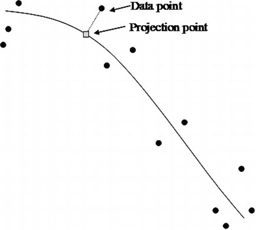
The principal curve is a one-dimensional curve that passes through d-dimensional data. The one-dimensional curve in d-dimensional space ℜ d is defined as a vector function f(δ) of a single scalar variable δ and δ provides an ordering along the curve (CitationHastie and Stuetzle, 1989). Consider a data set s consisting of n observations in ℜ d , f is the principal curve of s if
The principal curve of data s of size n is found using the following algorithm (CitationHastie and Stuetzle, 1989).
Initialization: | |||||
Find f
0(δ) = | |||||
Repeat: | |||||
Find δ f i (s j ),j = 1, …, n. | |||||
Find f (i + 1)(δ). | |||||
Until | d i + 1− d i | is less than a criterion, where d i = ∑ j = 1 n | |s j − f i (δ f i (s j ))| |2. | |||||
The principal curve of s is obtained by the iterative steps of finding a curve, f(δ), and the projection index of each data point, δ f i (s j ), j = 1, …, n. The algorithm stops when there is little improvement in the sum of squared distances between the data points and the curve.
The density of the principal curve is written as (CitationStanford and Raftery, 2000)
2.4. Spatial non-homogeneous Poisson process
The distribution of global defects is modeled by the spatial non-homogeneous Poisson process. The properties of the spatial non-homogeneous Poisson process are described by its intensity function, which governs the likelihood of an observation occurring at a location s. Consider the spatial non-homogeneous Poisson process that models the global defect distribution on a wafer surface, D ∈ ℜ2,{N(D):| D| ≥ 0}. Herein, N(D) is the number of defects on D. The intensity function at location s∈ D, λ (s| θ 0), is defined as λ (s| θ 0) = lim |d s|→ 0 E[N(d s)]|d s|, where E[N(d s)] is the expected number of defects on an infinitesimal region around s, Ds (CitationDiggle, 1983). In this study, we assume a quadratic intensity function, namely:
The density of the spatial non-homogeneous Poisson process is (CitationDiggle, 1983):
3. Clustering algorithm
In the previous section, we discussed the new mixture distribution proposed to model the defect distributions on wafer surfaces. In this section, we consider the problem of estimating the unknown model parameters p 0, …, p G , u 1, …, u G and θ 0, …, θ G . The number of local defect clusters, G, also needs to be estimated. In this study, we use the CEM algorithm for parameter estimation and the BIC for model selection.
3.1. CEM algorithm for clustering
Let us introduce latent variables z i = (z i0, z i1, …, z iG ), i = 1, …, n, which satisfy:
Assuming the number of the local defect clusters G is fixed, the following iterative steps are applied to estimate the model parameters.
At the mth iteration:
Step 1. E-step Compute | |||||||||||||||||||||||||||||||||||
Step 2. C-step Partition the defects into clusters according to | |||||||||||||||||||||||||||||||||||
Step 3. M-step
| |||||||||||||||||||||||||||||||||||
Steps 1–3 are repeated until convergence criteria are satisfied.
It is necessary to distinguish the linear clusters from the ellipsoidal clusters. In order to do so, we compute the eigenvalues of Σ k for all clusters with u k = 1. If for a cluster, one eigenvalue of its variance-covariance matrix is much smaller than the other one, it will be identified as a linear cluster. In this study, a cluster is identified as a linear cluster if one eigenvalue of its variance-covariance matrix is less than 5% in magnitude than the other eigenvalue.
3.2. Number of clusters
Finding the number of clusters is a crucial part of a model-based clustering analysis. There are many criteria proposed in the literature for model selection, such as information complexity (CitationBozdogan, 1993) and the BIC, etc. In this study, we choose the BIC as our model selection criterion because it is very simple and has been widely supported in the model-based clustering literature (e.g., CitationDasgupta and Raftery (1998) and CitationHwang and Kuo (2007)).
The BIC is approximated as (CitationSchwarz, 1978):
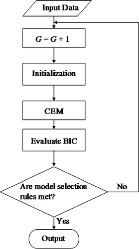
presents the flow-chart of the clustering algorithm using the CEM and the BIC. The algorithm has a loop with respect to the number of local defect clusters. Within that loop, the k-means clustering algorithm is applied to provide an initial clustering of the defects.
Fig. 2 Flowchart of the clustering algorithm.
4. Simulation
This section presents the clustering results obtained when the algorithm is applied to two simulated cases. In the simulation studies, the diameter of the wafers is 20 cm. The global defects are simulated from the spatial non-homogeneous Poisson process using a thinning method (CitationDiggle, 1983). The intensity function used in the global defect generation is quadratic, that is
The local defects in a cluster with a curvilinear pattern are generated from the assumption that the defects are distributed uniformly along and about an arc. The local defects in a cluster with an ellipsoidal pattern are created by sampling from the bivariate normal distributions with random variance-covariance matrices. Each local defect cluster has 100 local defects.
The algorithm is coded using MATLAB and executed on a computer with Pentium 4 3.0 GHz CPU and 1024 Mb RAM. The computational times are calculated using the cputime function in MATLAB. In order to measure the performance of the clustering algorithm, we define the misclassification rate as
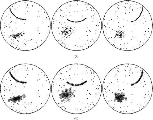
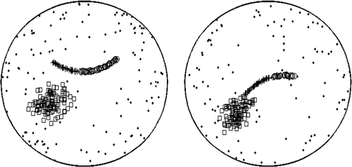
In simulation case 1, defect patterns on ten wafers are simulated. shows three representative patterns. Two local defect clusters, one with a curvilinear pattern and one with an ellipsoidal pattern, are generated on each wafer. The mean vector of the bivariate normal distribution, which is used to generate the ellipsoidal cluster, is assumed to be random in the rectangular region {(x,y): − 4 < x < − 2, − 4 < y < − 2}, where (0, 0) is the center of the wafer. The local cluster with the curvilinear pattern is randomly generated in the region {(x,y):y > 0}. Note that the two local clusters generated in this case are always separated, that is, they are not closely adjacent or overlapped. The clustering algorithm successfully finds the correct number of local defect clusters and identifies the correct pattern for each local cluster for all ten wafers. displays the clustering results for the three representative wafers.
Fig. 3 Three representative patterns of simulation case 1: (a) original defect patterns; and (b) clustering results.
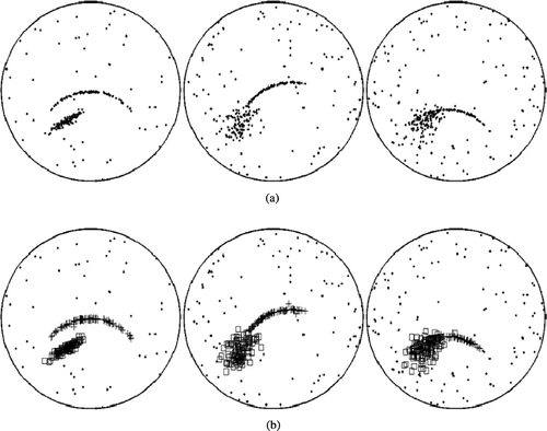
In simulation case 2, we also generate defect patterns on ten wafers. On each wafer, two local defect clusters, one with a curvilinear pattern and one with an ellipsoidal pattern, are closely adjacent or overlapped. Three representative wafers are shown in . The two local defect clusters on the first wafer are closely adjacent but not overlapped; the two local clusters on the second wafer are slightly overlapped while the two on the third wafer are highly overlapped. presents the clustering results of the algorithm applied to the three representative wafers. For all ten wafers, the clustering algorithm finds the correct number of local defect patterns. For the first two wafers shown in , the algorithm identifies the correct pattern for each local defect cluster, while for the third wafer, the algorithm assigns an ellipsoidal pattern and a linear pattern to the two local defect clusters, respectively. This indicates a limitation of the algorithm proposed in this paper. Since the proposed clustering approach clusters the defects only according to their spatial locations, it may not perform well when two or more defect clusters are highly overlapped.
Fig. 4 Three representative patterns of simulation case 2: (a) original defect patterns; and (b) clustering results.
For the purpose of comparison, the two-step algorithm developed by CitationHwang and Kuo (2007) is applied to analyze the wafers of these two cases. The two-step algorithm overestimates the number of clusters for all of the ten wafers in case 1 and six of the ten wafers in case 2. It tends to partition a curvilinear cluster into two or more pieces and model each piece by a bivariate normal distribution or a principal curve. shows typical clustering results of the two-step algorithm applied to the two cases.
Fig. 5 Typical clustering results using the two-step algorithm.
summarizes the averaged computational times and the averaged misclassification rates of the new algorithm and the averaged computational times of the two-step algorithm applied to the two simulation cases. As seen from the table, the algorithm is able to analyze one wafer within about 75 seconds. The two-step algorithm, however, needs about 547 seconds to analyze one wafer. When the local defect clusters are separated, the proposed algorithm has a very high accuracy. As the distance between the two local clusters decreases, the accuracy of the new algorithm decreases. However, most of the local defects are identified by the new algorithm. Note that the misclassification rate of the two-step algorithm is not calculated because the two-step algorithm overestimates the number of defect clusters for most of the wafers and there is not a proper way to compute the misclassification rate when the estimated number of clusters is not correct.
Table 1 Summary of the performance of the clustering algorithms
5. Conclusions
This paper proposes an automatic method for defect pattern recognition via model-based clustering for semiconductor fabrication process control. A mixture model is proposed to model the distribution of defects on semiconductor wafers. The proposed mixture model uses the spatial non-homogeneous Poisson process to model distribution global defects generated by assignable causes. The distributions of local defects are modeled by either the bivariate normal distribution or the principal curve. A clustering algorithm using the CEM for parameter estimation and the BIC for model selection is developed. Simulation studies prove that the new algorithm is fast and that it performs well. The clustering results will not only help the manufacturer monitor the manufacturing process but also provide valuable information for yield estimation.
Biographies
Tao Yuan received a Bachelor of Engineering degree in Thermal Engineering at Tsinghua University, Beijing, China in 2000, and a Master of Science degree in Aerospace Engineering and a Master of Engineering degree in Industrial Engineering at Texas A&M University, College Station, in 2003 and 2004, respectively. He is currently pursuing a Ph.D. degree in Industrial and Information Engineering at the University of Tennessee, Knoxville. His research interests are in statistical yield/reliability analysis of micro-/nano-electronics.
Way Kuo is University Distinguished Professor and Dean of Engineering at the University of Tennessee. Previously, he was with Texas A&M University and Bell Labs. He is an elected member of the US National Academy of Engineering, Academia Sinica, Taiwan and the International Academy for Quality. He has co-authored five textbooks and currently serves as Editor of IEEE Transactions on Reliability. He is a Fellow of IIE, ASQ, INFORMS, IEEE and the National Quality Institute.
Acknowledgements
The authors would like to thank the referees for valuable comments. The research is partially supported by NSF project DMI-0429176.
References
- Banfield , J. D. and Raftery , A. E. 1992 . Ice floe identification in satellite images using mathematical morphology and clustering about principal curves . Journal of the American Statistical Association , 87 : 7 – 16 .
- Banfield , J. D. and Raftery , A. E. 1993 . Model-based Gaussian and non-Gaussian clustering . Biometrics , 49 : 803 – 821 .
- Bensmail , H. , Celeux , G. , Raftery , A. E. and Robert , G. P. 1997 . Inference in model-based cluster analysis . Statistics and Computing , 7 : 1 – 10 .
- Bozdogan , H. 1993 . “ Choosing the number of component clusters in the mixture model using a new informational complexity criterion of the inverse Fisher information matrix ” . In Information and Classification , Edited by: Opitz , O. , Lausen , B. and Klar , R. 40 – 54 . Heidelberg , , Germany : Springer-Verlag .
- Campbell , J. G. , Fraley , C. , Murtagh , F. and Raftery , A. E. 1997 . Linear flaw detection in woven textiles using model-based clustering . Pattern Recognition Letters , 18 : 1539 – 1548 .
- Chen , F.-L. and Liu , S.-F. 2000 . A neural-network approach to recognize defect spatial pattern in semiconductor fabrication . IEEE Transactions on Semiconductor Manufacturing , 13 : 366 – 373 .
- Daley , D. J. and Vere-Jones , D. 1988 . An Introduction to the Theory of Point Processes , New York , NY : Springer-Verlag .
- Dasgupta , A. and Raftery , A. E. 1998 . Detecting features in spatial point processes with clutter via model-based clustering . Journal of the American Statistical Association , 93 : 294 – 302 .
- Diggle , P. J. 1983 . Statistical Analysis of Spatial Point Patterns , London , , UK : Academic Press .
- Gleason , S. S. , Tobin , K. W. , Karnowski , T. P. and Lakhani , F. 1998 . Rapid yield learning through optical defect and electrical test analysis . Proceedings of SPIE – The International Society for Optical Engineering , 3332 : 232 – 242 .
- Hansen , C. K. and Thyregod , P. 1998 . Use of wafer maps in integrated circuit manufacturing . Microelectronics Reliability , 38 : 1155 – 1164 .
- Hastie , T. and Stuetzle , W. 1989 . Principal curves . Journal of the American Statistical Association , 84 : 502 – 516 .
- Hwang , J. Y. 2004 . Spatial stochastic processes for yield and reliability management with applications to nano electronics , Ph.D. dissertation College Station , TX : Texas A&M University .
- Hwang , J. Y. and Kuo , W. 2007 . Model-based clustering for integrated circuit yield enhancement . European Journal of Operational Research , 178 ( 1 ) : 143 – 153 .
- Kuo , W. , Chien , K. W. and Kim , T. 1998 . Reliability, Yield and Stress Burn-in: A Unified Approach for Microelectronics Systems Manufacturing and Software Development , Boston , MA : Kluwer Academic Publishers .
- Kuo , W. and Kim , T. 1999 . An overview of manufacturing yield and reliability modeling for semiconductor products . Proceedings of the IEEE , 87 ( 8 ) : 1329 – 1346 .
- Schwarz , G. 1978 . Estimating the dimension of a model . Annals of Statistics , 6 : 461 – 464 .
- Shankar , N. G. and Zhong , Z. W. 2005 . A new rule-based clustering technique for defect analysis . Microelectronics Journal , 36 : 718 – 724 .
- Stanford , D. C. and Raftery , A. E. 2000 . Finding curvilinear features in spatial point patterns: principal curve clustering with noise . IEEE Transactions on Pattern and Machine Intelligence , 22 : 601 – 609 .
- Wang , C. H. , Kuo , W. and Bensmail , H. 2006 . Detection and classification of defect patterns on semiconductor wafers . IIE Transactions , 39 : 1059 – 1068 .