
 ?Mathematical formulae have been encoded as MathML and are displayed in this HTML version using MathJax in order to improve their display. Uncheck the box to turn MathJax off. This feature requires Javascript. Click on a formula to zoom.
ABSTRACT
We present here a compact liquid crystal (LC) based tunable notch filter with a narrow 3 dB bandwidth and a high quality factor. The structure of the proposed filter consists of two embedded resonators in serial, with an impedance adaptor and linear taper at each port. The notch filter combines tunable dielectric material LC with inverted microstrip technology, and was designed, fabricated and characterized to deliver a continuously tuned rejection frequency range from 3.545 GHz to 3.731 GHz, together with a narrow 3 dB bandwidth of ∼ 0.8 GHz and a high quality factor of ∼ 4.6. Such a notch filter is both compact (41 mm × 13 mm) and light weight (18.08 grams, including SMA connectors). It is suitable for working in the S band to suppress WiMAX signals that may cause interference in UWB communication systems. The narrow stopband and high quality factor of the device can be further improved at the expense of a certain extent of tuning efficiency, by using a thicker LC layer, and this is verified in experiment. The measured results of the proposed devices confirm the feasibility of using the current LC technology to manufacture tunable notch filters with a narrow bandwidth and a high quality factor.
1. Introduction
Liquid crystal (LC) materials have been attracting attentions as excellent electro-optic materials for the low driving voltage, low power consumption, and a high degree of anisotropy (in shape, dielectric and optical). Nowadays, LCs have been demonstrated in a plenty of applications, such as LC based flat panel displays, optical fibers, photonic metamaterials, memory devices, etc. [Citation1–6]. Over the last twenty years there has been growing interest in their use LCs as tunable dielectrics for microwave (MW) applications. LC based tunable phase shifters, filters, capacitors, resonators, and antennas have been extensively developed [Citation7–12]. Bandstop filters (BSFs) are key devices for MW systems due to their ability to attenuate unwanted signals. BSFs with a narrow stopband and a high quality factor, known as notch filters, are particularly useful for suppressing spurious frequencies and noise signals [Citation13,Citation14]. BSFs with reconfigurable characteristics, such as those adopting LC technology, are even more attractive for further extending the potential of MW systems [Citation8,Citation13,Citation15].
LC based BSFs with narrow bandwidths have been achieved by optimizing filter structures to overcome the effect of the losses due to the LC material. For instance, a LC based BSF possessing a relatively wide stopband was reported in [Citation15], suggesting that LC materials are not suitable for use in obtaining a narrower stopband due to their high dielectric loss in the working frequency range. However, according to [Citation13], when using conventional spurline structures, LC based notch BSF devices exhibited narrow stopbands. Another LC based BSF was proposed with an unconventional spiral spurline structure that further narrowed the stopband bandwidth [Citation8]. With the development of LC technology, more and more LC materials with high anisotropy and low dielectric loss have been used in MW systems. The development of LC based MW devices with much improved performances can therefore be expected, and how to achieve the desired performances of tunable notch filters in the S band (2–4 GHz) by using the current LC technology needs to be investigated.
In this work, we will present a narrow stopband BSF that incorporates a high anisotropic LC material with low dielectric loss and an optimized ML structure. The proposed BSF would be of practical use in MW applications due to its advantages over several existing LC based BSFs. Firstly, its compact structure makes it more suited to integrate into microstrip antenna edges, and many other satellite communications applications [Citation16]. Secondly, the high Q factor of this embedded spurline BSF structure is particularly useful for filtering out spurious frequencies and noise signals without too much influence on the required signals, due to it producing less radiation than other conventional shunt-stubs and coupled structures [Citation13,Citation17]. Another benefit of this embedded spurline structure based BSF is the ease of its manufacture and integration.
Ultra-wideband (UWB, 3.1–10.6 GHz) technology is very attractive and promising as a form of transmission that occupies a very wide bandwidth to offer high data transmission rates for applications such as short-range high-throughput wireless communications, and medical imaging [Citation13,Citation18]. The fact that UWB transmissions cross the boundaries of some currently licensed frequency bands implies that UWB transmission may cause interference. This raises the need for BSFs with extremely narrow stopbands to attenuate unwanted inference signals. The BSF reported here was particularly designed to attenuate the interference of Worldwide interoperability for Microwave Access (WiMAX, 3.3–3.6 GHz) in the UWB range of applications.
2. Filter structure and design procedure
The device configuration of the proposed LC based narrowband BSF is depicted in Figure . LC material is sandwiched between an aluminium metal ground and Rogers 4003C, of which the relative permittivity , the dielectric loss
, and the thickness
. The BSF ML structure formed on the Rogers substrate is inversely configured to face the LC layer. The ML is 0.017 mm thick. The ground plane is etched to insert the SMA contact and for ease of fabrication. Due to the liquid-like state of the LC, the SMA contact doesn’t touch the LC layer directly, hence the impedance adaptors at both ends with width
shown in Figure are designed to eliminate the impedance mismatch caused by the change in substrate between the air and the LC material [Citation19]. The best impedance match that could be obtained by simulation has a width of
, and
. The linear taper lines with length
at both ends were adjusted to cope with the change in ML width in order to minimize any induced reflection.
Figure 1. Schematic diagram of the proposed LC based tunable narrowband BSF.
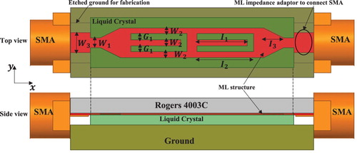
The final dimensions of the designed device structure are: ,
,
, and
. The proposed LC based narrowband BSF is capable of continuously and selectively attenuating the licensed WiMAX bands by driving the LC material. The following sections describe the design strategy and the measured characteristics of the fabricated BSF.
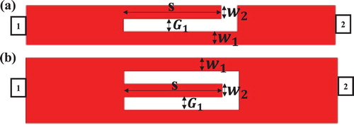
2.1. Theoretical analysis and comparison of spurline and embedded spurline structure units
Spurline structures shown in Figure (a) are commonly used to form BSFs, and the structures have in the past been studied in detail and used for LC based tunable bandstop filters [Citation8,Citation13]. However, the use of an embedded spurline structure, as shown in Figure (b), to produce a narrow bandstop performance has been less adequately investigated. The working principle behind these two structures is based on a general interference theory of transmitted and reflected waves, as shown in Equations (1)–(4) below. By adjusting the resonator length S and the effective relative permittivity of its substrate, a quarter-wavelength resonator can be designed to target a central frequency .
(1)
(1)
(2)
(2)
(3)
(3)
Figure 2. Prototype of (a) Spurline structures and (b) embedded spurline structures.
When n = 0:
(4)
(4) where
and
are the guided wavelength at the stopband center frequency,
, and the effective relative permittivity of its substrate, respectively. In Equation (1),
indicates that there is a 180° difference between the phases of the waves, which means that they are in anti-phase. One of the key design strategies in order to obtain a high Q factor and a narrow stopband bandwidth for the BSF is choosing a suitable resonator structure. To achieve this, we carried out a comparative analysis of the performance characteristics of the two structures.
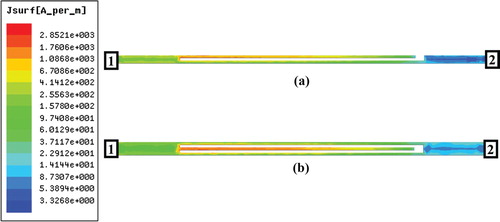
Figure is the simulated transmission and reflection characteristics of the BSFs with the same substrate and resonator dimensions as shown in Figure . It shows that the embedded spurline structure has a narrower 3 dB stopband than that of the spurline structure. The current density distribution on each filter structure further supports such behaviors. Figure displays the current density distribution of both structures with the same dimensions at the rejection frequency of 3.725 GHz, where the color index represents the amplitude of the current density. At the rejection frequency of 3.725 GHz, their currents are not equally distributed. The low current densities at the outputs indicate that these structures sharply reject the 3.725 GHz signal. As the quarter-wavelength resonators each have the same width
, the current density of the resonator part with length
can be compared to estimate the stored MW energy of these two structures. The embedded spurline structure has a higher current density due to the stronger coupling between the resonator part and its main transmission lines, which results in a narrower stopband and a larger Q factor.
Figure 3. S-parameters comparison of the spurline and embedded spurline structure prototype.
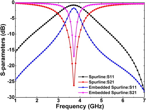
Figure 4. Current distribution at the rejection frequency of 3.725 GHz for (a) the spurline structure and (b) embedded spurline structure prototype.
2.2. Theoretical analysis of the notch characteristics of the embedded spurline unit
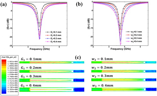
Based on the above discussion, the embedded spurline type was selected due to its high Q factor and narrow stopband bandwidth. The next step was to analyse the effects of its dimensions (gap, and width
of the resonator) on the performances of the BSF. The effects on the gap and width on the stopband are shown in Figure (a and b) for the nominal values
. Their current distributions are shown in Figure (c). The total amount of stored energy can be calculated by integrating the current density. A smaller gap
, and a smaller resonator width
led to a more concentrated current on the resonator section, which results in a smaller stopband bandwidth and a larger Q factor, as shown in Figure (a) and (b).
Figure 5. The effects of (a) gap , and (b) resonator width
, for the notch characteristics of the embedded spurline unit, and (c) current distributions at a stopband frequency of 3.725 GHz.
2.3. Optimization of the filter structure
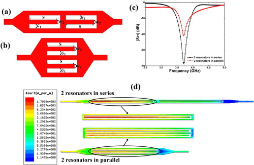
In spite of the high Q factor, the rejection level of the embedded spurline structure was around −20 dB, as shown in Figure . In order to improve the rejection level and also meet the impedance requirement, tapered line technology and multiple embedded spurline resonators were used. Initially two structures were proposed. One used two embedded resonators in series, and the other configuration used them in parallel, as shown in Figure (a and b). Figure (c) shows the transmission of BSFs incorporating these two structures, with nominal values of
. Figure (d) shows the current distributions of each of the structures. The performance of the serially embedded resonator based BSF was clearly much better than that of the parallel structure based BSF, both in terms of the Q factor and the rejection level.
Figure 6. Comparison of structures with two embedded spurline units (a) in series and (b) In parallel, and (c) transmission, and (d) Current distributions.
2.4. Analysis of the effect of the LC material for notch characteristics
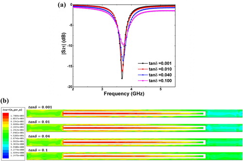
The influence of the LC material losses on MW device performances is often significant and cannot be ignored. In general, in a high frequency regime (>10 GHz), LC materials have the advantage over some conventional tunable materials, such as ferroelectrics, in terms of low material losses. At frequencies below 10 GHz, however, LC materials are relatively lossy. Considering the working frequency range (3–4 GHz) of the designed BSF, it is necessary to select the appropriate LC materials for performance of the BSF. Therefore, the effects of the LC material dielectric loss tangent on the LC based BSF performance were studied.
This analysis was carried out for the single embedded spurline structure shown in Figure (b), with the nominal values of . As a guiding principle, the results should be applicable to the eventual structure. Figure (a) shows the simulated transmission properties when varying the material loss tangent, and indicates that increasing the loss tangent of the LC material is detrimental to both the rejection level and the Q factor. For
, the material loss effect on attenuation and the Q factor tended to become saturated, which indicates a limitation to the required material loss for improvement of the quality of the BSF. That is, LC materials with a dielectric loss tangent ∼ 0.01 are good enough for use in narrow stopband BSF design. The current distribution presented in Figure (b) complementally shows how the current density gradually changes with a decrease in the LC loss tangent to improve the Q factor and attenuation at the rejection frequency. Based on the analysis, the LC material GT3-24002 (Merck) was chosen for its acceptably low dielectric loss and high dielectric anisotropy. Its material properties at 10 GHz and 23°C are as follows:
,
,
, and
. The regulating of dielectric permittivity between
and
under the control of external bias voltage leads to the continuous tuning of filter’s central frequency
according to the equation (4).
Figure 7. (a) The transmission characteristics of the embedded spurline unit, and (b) Current distributions at the rejection frequency, when varying the LC dielectric loss tangent .
3. Implementation and experimental results
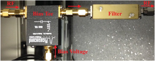
The proposed BSF was fabricated with the structure shown in Figure . The fabricated device had a compact size of 41 mm (L) by 13 mm (W), and a light weight of 18.08 grams. The frequency response of the filter was characterized by measuring the scattering parameters using a one-port vector network analyser (VNA) Agilent 8722ET. Figure shows the measurement setup for the fabricated device. A square wave signal of 5 Hz was applied through a bias tee to switch the LC molecules, and subsequently regulate the performance of the filter.
Figure 8. Experimental setup for measurement.
The measured transmission for various bias voltages is shown in Figure (a). The rejection frequency of the fabricated BSF was 3.731 GHz under a zero bias voltage, corresponding to the lowest relative permittivity value
of the LC material. By enlarging the bias voltage, the resulting increase in the LC relative permittivity led to a decrease in the rejection frequency. The minimum rejection frequency of 3.545 GHz was achieved when a voltage of 20 Vrms was applied, when the LC layer was assumed to possess the largest relative permittivity
. The total tuned frequency range was 186 MHz, together with a tunability of 5.2% relative to the center frequency of 3.545 GHz when fully biased. Figure (b) shows the rejection center frequency as a function of the LC bias voltage, indicating a nonlinear decrease in the rejection frequency as the applied voltage increases. The bias voltage range for obtaining a tuning of 11.3%–83.3% for the rejection frequency was 8 Vrms, from 4 Vrms to 12 Vrms.
Figure 9. Measured results of the device with respect to the LC bias voltage: (a) Transmission, (b) stopband rejection frequency, and (c) stopband 3 dB bandwidth and Q factor.
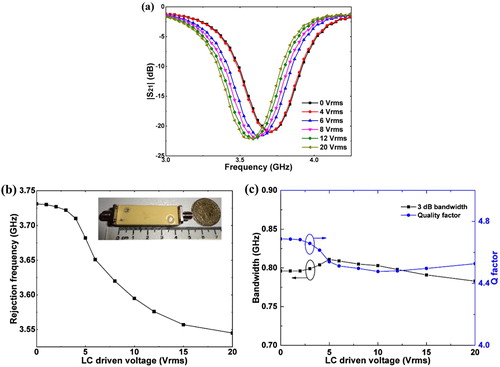
According to the measured results shown in Figure (a), the rejection level of the fabricated BSF reached ∼ 22 dB, and remained almost unchanged when tuned from 0 Vrms to 20 Vrms. Little variation was also found for the stopband 3 dB bandwidth and quality factor (Q factor) shown in Figure (c), and both features are desirable for real applications. The average values of the 3 dB bandwidth and Q factor were 0.8 GHz and 4.6, respectively. The achieved 3 dB bandwidth and Q factor of the fabricated BSF were better than that of existing LC based BSFs with stub or spurline structures, and the result shows good agreement with the theoretical analysis [Citation8,Citation13,Citation20].
In order to experimentally verify the effect of LC layer thickness on the device performance, the embedded BSFs were built based on other two various LC layer thickness of and
, regardless of the impedance mismatching due to the change of LC layer thickness. The measured transmission properties of the three devices under the unbiased state and at a bias voltage of 20 Vrms are shown in Figure (a). Figure (b) shows the measured stopband 3 dB bandwidth. For the design with the LC layer thickness of
, its stopband 3 dB bandwidth is the smallest (∼ 0.6 GHz) due to its lowest overall loss, though there is a worse reflection because of the impedance mismatching. The fabricated devices with different thicknesses of the LC layer indicate that it is possible to optimize and achieve a narrower stopband at the expense of a certain extent of tuning efficiency, depending on specific project requirements. A comparison between this work and those LC based notch filters that were reported recently for C-band and S-band applications is presented in Table . It is expected that the device with
-thick LC layer would have a narrower 3 dB stopband and a higher Q factor when it meets the
impedance matching. In addition, the improvement in the fabrication process such as smaller LC thickness variation could ameliorate device performance, and also lead to a better agreement on the measurement and numerical results.
Figure 10. Measured results of devices with three LC layer thicknesses: (a) Transmission under 0 and 20 Vrms bias voltage, and (b) stopband 3 dB bandwidth with respect to various LC bias voltages.
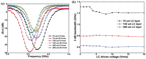
Table 1. Comparison with recently reported LC based notch filters
The implementation of the BSF device suggests that it is possible to produce LC based BSFs with very narrow stopbands in the low MW frequency range (< 10 GHz), as long as suitable resonator structures are designed and an LC material that has a low dielectric loss is used. As LC technology develops, we expect that the performance of this LC based notch BSF, with its high Q factor and narrow stopband, will be further improved. The fabricated device is suitable for practical use in attenuating and suppressing the WiMAX signal that may cause interference in UWB systems.
4. Conclusions
This work demonstrates an innovatively designed tunable notch BSF based on tunable LC dielectric material. Experiments have shown that good device performance can be achieved through optimization of the filter structure using two serially embedded spurline resonators, and by selecting an LC material with low dielectric loss. The resulting filter was fabricated in an inverted microstrip structure using tapered line technology. Achieving the narrow 3 dB bandwidth of ∼ 0.8 GHz, the high Q factor of ∼ 4.6, and the acceptable rejection level of ∼22 dB, the fabricated device provides an improved notch filter performance in comparison to other LC based BSFs reported in the literature. The proposed BSF also has desirable features such as both the measured 3 dB bandwidth and the Q factor remaining almost constant upon various external voltages. The ability of the BSF to tune the rejection frequency from 3.545 GHz to 3.731 GHz with high a Q factor makes it an ideal candidate to effectively suppress WiMAX signals for UWB applications. The device with -thick LC layer was rebuilt with various LC layer thickness of
and
, and it indicates that the narrow stopband and high quality factor of the device can be further improved at the expense of a certain extent of tuning efficiency, by using a thicker LC layer. The performance of the proposed devices have confirmed the feasibility of using current LC technology to make tunable notch filters with good bandwidth and a good Q factor. With its tunable characteristics, narrow stopband, high Q factor, good attenuation, light weight, and simple and compact structure, the designed LC based notch filter is attractive for use in MW applications.
The filter structure used here can be found in many research works, as it’s a well-known quarter-wavelength resonator in conventional microwave field (as referenced in the original manuscript). While in this work, structural changes have to be made in order to achieve a compact tunable notch filter with a narrow 3 dB bandwidth and a high quality factor, especially in the case of using LC materials as the substrate (generally LC has relatively higher dielectric loss than conventional untuned substrates). Therefore, the geometrical parameters of the altered structure are investigated. Two quarter-wavelength resonators with series or parallel layout are also studied to improve the device rejection level while maintain its high quality factor. In addition, impedance adaptors and taper lines are adopted in order to adjust to the LC fabrication techniques.
In addition, we have demonstrated the feasibility of using the current LC technology to manufacture tunable notch filters with a narrow bandwidth and a high quality factor. Owing to the relatively high dielectric loss of LC materials in frequencies lower than 10 GHz, previous LC based bandstop filters in literature usually possess worse quality factors. As the growth of LC technology, some types of LC materials with better quality have been developed, therefore investigating how the performances of tunable notch filters in the S band can be achieved by using the current LC technology is essential and meaningful. Hence, in this work we adopt a new LC material with a high anisotropy and a low dielectric loss to design a tunable notch filter for suppressing WiMAX signals in UWB applications. By optimizing the device from both of LC material side and structural parameters, the designed filter has been shown to have a narrow 3 dB bandwidth and a high quality factor.
Acknowledgements
The authors would like to thank the UK Engineering and Physical Sciences Research Council (EPSRC) for the support through the EPSRC Center for Innovative Manufacturing in Ultra Precision (EP/I033491/1). L.C. thanks Chinese Scholarship Council and Cambridge Commonwealth, European & International Trust, and the Natural Science Foundation of Jiangsu Province, China (Grant No. BK20180364) for financial support.
Disclosure statement
No potential conflict of interest was reported by the authors.
ORCID
Daping Chu http://orcid.org/0000-0001-9989-6238
Additional information
Funding
References
- Ghasemi M, Choudhury PK. Propagation through complex structured liquid crystal optical fibers. J. Nanophotonics. 2014;8:083997-1–083997-13. doi: 10.1117/1.JNP.8.083997
- Buchnev O, Podoliak N, Kaczmarek M, et al. Electrically controlled nanostructured metasurface loaded with liquid crystal: toward multifunctional photonic switch. Adv. Opt. Mater. 2015;3:674–679. doi: 10.1002/adom.201400494
- Ghasemi M, Choudhury PK. On the conducting sheath double-helix loaded liquid crystal optical fibers. J. Electromagn. Waves Appl. 2015;29:1580–1592. doi: 10.1080/09205071.2015.1053575
- Ghasemi M, Choudhury PK. Conducting tape helix loaded radially anisotropic liquid crystal clad optical fiber. J. Nanophotonics. 2015;9:93592. doi: 10.1117/1.JNP.9.093592
- Prakash J, Chandran A, Biradar AM. Scientific developments of liquid crystal-based optical memory: a review. Reports Prog. Phys. 2016;80:16601. doi: 10.1088/0034-4885/80/1/016601
- Su H, Wang H, Zhao H, et al. Liquid-crystal-based electrically tuned electromagnetically induced transparency metasurface switch. Sci. Rep. 2017;7:17378. doi: 10.1038/s41598-017-17612-7
- Fritzsch C, Bildik S, Jakoby R. Ka-band frequency tunable patch antenna. Proc. 2012 IEEE Int. Symp. Antennas Propag; 2012.
- Torrecilla J, Avila-Navarro E, Marcos C, et al. Microwave tunable notch filter based on liquid crystal using spiral spurline technology. Microw. Opt. Technol. Lett. 2013;55:2420–2423. doi: 10.1002/mop.27812
- Bulja S, Mirshekar-Syahkal D. Meander line millimetre-wave liquid crystal based phase shifter. Electron. Lett. 2010;46:769–771. doi: 10.1049/el.2010.3513
- Yeh JA, Chang CA, Cheng C-C, et al. Microwave characteristics of liquid-crystal tunable capacitors. IEEE Electron Device Lett. 2005;26:451–453. doi: 10.1109/LED.2005.851118
- Yaghmaee P, Fumeaux C, Bates B, et al. Frequency tunable S-band resonator using nematic liquid crystal. Electron Lett. 2012;48:798. doi: 10.1049/el.2012.1366
- Yaghmaee P, Karabey OH, Bates B, et al. Electrically tuned microwave devices using liquid crystal technology. Int J Antennas Propag. 2013;2013:1–9. doi: 10.1155/2013/824214
- Urruchi V, Marcos C, Torrecilla J, et al. Note: tunable notch filter based on liquid crystal technology for microwave applications. Rev Sci Instrum. 2013;84:26102. doi: 10.1063/1.4790555
- Mokhtaari M, Bornemann J. Microstrip ultra-wideband filter with flexible notch characteristics. Wirel Eng Technol. 2012;03:12–17. doi: 10.4236/wet.2012.31002
- Skulski J, Szymańska A. Liquid crystal tunable microwave band stop filters. Electron Technol. Conf. 2013. International Society for Optics and Photonics; 2013. p. 89022E–89022E.
- Sanchez-Hernandez D, Robertson I. Triple band microstrip patch antenna using a spur-line filter and a perturbation segment technique. Electron. Lett. 1993;29:1565–1566. doi: 10.1049/el:19931043
- Krishna JVSH. Compact spiral folded spurline for low-frequency applications. Electron Lett. 2011;47:S1. doi: 10.1049/el.2011.3292
- Allen B, Brown A, Schwieger K, et al. Ultra wideband: applications, technology and future perspectives. International Workshop on Convergent Technologies (IWCT); 2005.
- Cai L, Xu H, Li J, et al. High figure-of-merit compact phase shifters based on liquid crystal material for 1-10 GHz applications. Jpn J Appl Phys. 2017;56:11701. doi: 10.7567/JJAP.56.011701
- Cai L, Xu H, Chu D. Compact liquid crystal based tunable band-stop filter with an ultra-wide stopband by using wave interference technique. Int J Antennas Propagation. 2017;2017:1–11. doi: 10.1155/2017/9670965