Abstract
We present an improved detection scheme for a two-wave mixing interferometer with a Bi12SiO20 crystal. The proposed detection scheme allows quasi-balanced detection of ultrasonic signals whereby electrical disturbances are suppressed. Quasi-balancing is achieved by changing the polarity of the high voltage at the photorefractive crystal, leading to an inversion of the optical interference signal, in combination with inversion of the detector signal using a signal inverter before the data acquisition device. The polarity of the high voltage is changed by utilizing an H-bridge consisting of five high-voltage relays. Microcontrollers are used to synchronize the reversion of the high voltage at the photorefractive crystal and the inversion of the measured signals. We demonstrate remote measurement of ultrasonic waves and shown that electrical disturbances are suppressed using the quasi-balanced mode.
1. Introduction
We present an enhanced two-wave mixing interferometer (TWMI) setup for optical contactless detection of ultrasound waves. A TWMI enables remote ultrasound detection on rough surfaces Citation1Citation2Citation3Citation4Citation5 and has therefore found application in different fields. While TWMIs are found mainly in diverse non-destructive testing applications using laser ultrasonic techniques Citation[6], other applications have also been demonstrated. For example, by utilizing a TWMI, the potential of remote photoacoustic imaging for industrial applications on solid materials Citation[7] and for biomedical applications on skin Citation[8] has been shown.
Acquiring ultrasound remotely and without physical contact by optical means offers several advantages. Firstly, remote detection permits measurements on hot or corrosive surfaces, which could damage contacting transducers. Secondly, due to the non-contacting nature of the technique, the specimen is not contaminated via the transducer or coupling agent. This is important for many in-line process applications, but also in aeronautics contacting evaluation means are often prohibited. In biomedical applications, critical areas like open wounds or other parts have to be kept sterile while examined and non-contacting examination methods are therefore preferable. Contactless methods permit evaluation of fragile samples and do not alter the shape of the examined specimen. This is often not possible if a contacting transducer is attached to a specimen. Additionally, optical means allow measurements of areas which are difficult to access, e.g. regions with a high curvature. A further advantage lies in the high detection bandwidth, compared to piezoelectric transducers, which can be achieved by using optical methods. Often the bandwidth is only limited by the detection electronics and measurement of signals up to the GHz range is possible. A high detection bandwidth goes hand-in-hand with high resolution, if the acquired signals are used for imaging purposes. As the optical detection beam can be focused to a very small spot size – approximating a point detector – high resolution imaging is possible.
Problems can, however, arise when electrical disruptions are present which disturb the ‘real’ signals. Such effects are often observed when using pulsed lasers for ultrasound generation, as commonly done in laser ultrasound or in photoacoustic imaging. For pumping the lasers flash lamps are widely used. Triggering of these flash lamps is done with high voltage pulses. This generates strong electrical noise, if not perfectly shielded against electromagnetic interference (EMI), which is than received by the detection electronic. In this work, we use a TWMI to remotely record ultrasonic waves on a surface and present an improved detection scheme which suppresses artifacts due to these electrical disruptions. Suppression of the artifacts is realized by introducing a quasi-balanced detection scheme based on the reversion of the high voltage on the photorefractive crystal.
2 Reversion of the high voltage
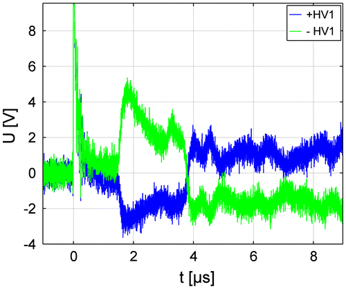
The TWMI setup used is based on a Bi12SiO20 (BSO) photorefractive crystal (PRC) with dimensions of 5 × 5 × 5 mm3 cut along the [1 1 0] and [ 1 0] crystallographic axes. To provide the highest sensitivity, the interferometer is operated in the drift regime by applying an electric field of 7 kV/cm in the [0 0 1] direction. By illuminating the crystal with two beams, i.e. reference beam and signal beam, a grating inside the crystal is formed Citation7Citation8. A part of the reference beam is then deflected in the direction of the transmitted signal beam with its wave front matched to the signal beam. The dynamic formation of the grating is defined by the specific time constant of the PRC. The crystal cannot adapt to changes which are faster than the time constant. If changes in the phase relation between signal and reference beam are faster a variation in the transmittance is observed. This can be used for measuring fast motions of surfaces and, therefore, for remote detection of ultrasonic signals. Such a signal is shown in Figure (blue curve). The detected ultrasound wave starts at 1.5 μs and is generated by a high-power pulse laser. The peak at the beginning of the signal is an electrical induced disruption generated by the same laser. If the high voltage at the PRC is reversed, i.e. the polarity is changed, the measured ultrasound signal is inverted, as shown by the green curve in Figure . Inversion affects only the signal originating from the change in the optical phase; the electrical disruption is not affected. This effect was used to develop a quasi-balanced setup which is less sensitive to electrical noise.
Figure 1 Effect on the signal when changing the polarity of the high voltage on the BSO crystal. (The color version of this figure is included in the online version of the journal.)
To understand the effect of the reversed voltage on the crystal in the following we will describe a simple model. A complete discussion would require description by a set of coupled differential equations which is out of scope of this paper and can be found, for example, in Picoli et al. Citation[9] or in Buse Citation[10].
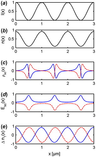
Two plane beams interfere in the crystal and form an intensity grating I(x), as depicted in Figure (a). In the bright areas, electrons are excited from donors to the conduction band and an electron density n(x), shown in Figure (b), is formed. If no external voltage is applied to the crystal, the electrons diffuse to the dark regions where they get trapped. Thus, bright areas are positively charged and dark areas negatively. If a voltage is applied to the crystal, in addition to the diffusion current a drift current arises. The direction of the drift current depends on the direction of the applied voltage. As a consequence, the resulting charge densities ρ(x) for positive and negative voltages are mirrored (Figure (c)). From Gauss’ law we know that the divergence of the electric field is proportional to the charge density. As a result, the space charge field ESC(x) is shifted 0 or π (blue and red line Figure (d)) relative to the intensity grating I(x) if the external voltage is larger than the diffusion field but smaller than the saturation field of the crystal Citation[1]. Finally, a refractive index grating is formed due to the Pockels effect. The change in refractive index is linearly proportional to the total electric field E (space charge field ESC + external field EA):(1) where n0 is the refractive index without illumination and reff is the effective electro-optic coefficient. The change in refractive index has thus the same shape as ESC(x), but inverted, and is therefore not depicted. Instead we show in Figure (e) the first Fourier component of Δn. For a positive voltage, the index grating has zero phase shift relative to the intensity grating; for a negative voltage a shift of π is observed.
Figure 2 The formation of an index grating due to an intensity grating in a photorefractive crystal: intensity grating (a), electron density (b), space charge (c), space charge field (d) and first Fourier component of the index grating (e). Positive voltage: blue solid lines, negative voltage: red dashed lines. (The color version of this figure is included in the online version of the journal.)
Each beam is refracted by the formed index grating Δn(x) in the direction of the other beam. In particular, we are interested in the refracted reference beam, which after the grating propagates in the direction of the signal beam. For a thick volume grating, an additional phase shift of π/2 has to be considered for the refracted beam. This finally leads to a phase shift of π/2 or 3π/2 between signal beam and refracted reference beam for positive or negative voltages, respectively Citation1Citation11. The signal beam and refracted reference beam are then directed to a photodiode. The phase shift between the two beams is either π/2 or 3π/2 in steady state. At these two points the intensity is at half maximum and a change in the relative phase leads to an increase or decrease of the intensity at the photodiode. For example, a positive change of phase leads to an increase of the signal if the two beams are shifted by π/2 and to a decreased signal for 3π/2. A fast motion of the surface changes the phase of the signal beam while the phase of refracted reference beam is not altered. This disturbance of the phase leads to a signal at the photodiode, the sign of which depends on the sign of the applied voltage.
3 Setup
In Figure (a), a schematic of the quasi-balanced TWMI setup is illustrated. As coherent light source, a frequency doubled Nd:YAG laser with a wavelength of 532 nm and 300 mW output power is used. To prevent damage of the optical devices the beam is expanded to 3 mm by a beam expander. At the polarizing beam splitter (PBS2), the beam is split into sample and reference beams. The ratio between the two beams can be controlled by a half wave plate (HW2). The reference beam is guided to the PRC; the signal beam is directed to the sample passing a second polarizing beam splitter (PBS3) and a quarter wave plate (QW1). Finally the signal beam is focused at the surface by a lens system (L1–L3). Reflected light is collected by the same lens system and passes the quarter wave plate again. As the quarter wave plate is passed two times the polarization of the light is rotated 90° relative to the input beam and is reflected by the polarizing beam splitter. Using a lens (L4), the beam is then focused through the PRC towards the detector D1 (New Focus 1801 125 MHz-Photoreceiver). Using a thin glass plate (TGP) a small portion of the reflected beam is directed to a second detector (D2) used to measure the collected light intensity. The signal of D2 can therefore be used for the positioning of the sample in the focus plane of lens L3 (highest signal of D2). Also, during the measurement the signal of D2 is an indicator for the surface characteristics. To reduce the thermal stress on the sample the detection laser is pulsed by a Q-switch, which consists of a Pockels cell (PC) and a polarizing beam splitter (PBS1). Controller C1 triggers the Q-switch and, 5 ms later, the excitation laser. After another 1 ms the Q-switch is turned-off and the laser is directed into a beam dump. The ‘on-time’ has to be sufficiently long to ensure that the grating is formed in the PRC and all ultrasonic signals are recorded. For generation of the ultrasound waves, a Nd:YAG excitation laser at its fundamental wavelength of 1064 nm with a duration of 9 ns was used.
Figure 3 Schematics of the quasi-balanced two-wave mixing interferometer setup (a) and of the voltage inverter H-bridge (b). (The color version of this figure is included in the online version of the journal.)
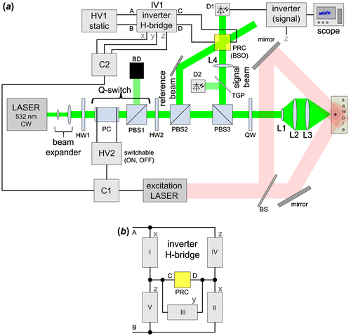
The quasi-balanced mode is realized by synchronized reversion of the high voltage and inversion of the measurement signal. In the proposed scheme, no additional PRC and/or photodetector are needed. Quasi-balancing is achieved by averaging at least two measurements, whereby half of the measurements are acquired at high voltage (+HV1) and the other measurements with the reversed high voltage (−HV1) applied at the PRC. Since at least two measurements are needed, the system works in ‘quasi-balanced’ mode. A second controller C2, which is synchronized to C1, is used to control the change of polarity of the high voltage. Voltage reversion is done by an H-bridge consisting of five relays (HM12-1A69-150, operating time 3 ms, maximum switching voltage 10 kV), as depicted in Figure (b). First, pin x is set to high level whereby relays I and II are closed. Pins y and z are set to zero, thus all other relays are open and the voltage HV1 is applied to the PRC. After the measurement pin x is set to zero and relay III is closed (pin y) for a few milliseconds to discharge the crystal. Finally, pin z is set to high level and the reversed voltage is applied to the PRC. Pin z is also connected to a switchable signal inverter located between detector D1 and the oscilloscope. A logic high level switches the signal inverter form non-inverting to inverting. Thus, when the high voltage is reversed the ultrasonic signal is inverted twice. First, due to the change of the electro-optical coefficient, as described in Section 2, and, second, by the electric signal inverter. As a result, the ultrasonic signal has the same shape for both polarizations of the high voltage. In contrast, the disturbance signal is inverted only once by the electrical signal inverter. To avoid post processing, the oscilloscope is set to averaging mode. By averaging a signal without electrical inversion at voltage +HV1 and a signal with electrical inversion at voltage –HV1 the disturbance signal gets subtracted, hence suppressed. The ultrasonic signal, on the other hand, is preserved.
4 Measurement
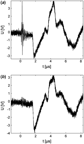
To test the setup, a weak ultrasound wave was generated inside a sample, consisting of a semitransparent polymer with an absorbing inclusion, via the photoacoustic effect Citation[7]. The oscilloscope was set to 20-times averaging. Ultrasound waves were remotely acquired on the surface of the polymer sample. First a measurement was performed without the quasi-balanced mode, as shown in Figure (a). An ultrasonic signal starting at 1.5 μs is clearly visible. However, a strong electrical disturbance at t = 0 is observed. Figure (b) shows the measurement using the quasi-balanced mode. The electrical disturbance is suppressed, though the ultrasonic signal at 1.5 μs is still present.
Figure 4 Comparison between normal measurement (a) and quasi-balanced measurement (b). Suppression of electrical noise at approx. 0.2 μs is observed.
5 Conclusion
We have demonstrated a simple extension for a two-wave mixing interferometer with a BSO crystal for quasi-balanced detection. The setup acquires ultrasonic waves remotely without physical contact to the specimen. Quasi-balancing was achieved by a synchronized reversion of the high voltage at the crystal and inversion of the measurement signal. We have shown that electrical disturbances can be suppressed by using the quasi-balanced mode. We have demonstrated the technique on a TWMI using a BSO crystal. However, the propose method should also work with other crystals like InP or CdTe when operated in the drift regime.
Acknowledgements
This work was supported by the Austrian Science Fund (FWF), project numbers S10503-N20 and P25584-N20, the Christian Doppler Research Association (Christian Doppler Laboratory for Photoacoustic Imaging and Laser Ultrasonics), the Federal Ministry of Economy, Family and Youth, the European Regional Development Fund (EFRE) in the framework of the EU-program Regio 13, and the federal state Upper Austria.
Related Research Data
References
- Kamshilin, A.A.; Romashko, R.V.; Kulchin, Y.N. J. Appl. Phys. 2009, 105, 031101.
- Honda, T.; Yamashita, T.; Matsumoto, H. Jpn. J. Appl. Phys. 1995, 34, 3737–3740.
- Pouet, B.; Ing, R.; Krishnaswamy, S.; Royer, D. Appl. Phys. Lett. 1996, 69, 3782–3784.
- Zamiri, S.; Reitinger, B.; Berer, T.; Bauer, S.; Burgholzer, P. Procedia Eng. 2010, 5, 299–302.
- Monchalin, J.P. Appl. Phys. Lett. 1991, 59, 3233–3235.
- Scruby, C.B.; Drain, L.E. Laser Ultrasonics – Techniques and Applications; Adam Hilger: Bristol, 1990; pp 152–156.
- Berer, T.; Hochreiner, A.; Zamiri, S.; Burgholzer, P. Opt. Lett. 2010, 35, 4151–4153.
- Hochreiner, A.; Berer, T.; Grün, H.; Leitner, M.; Burgholzer, P. J. Biophotonics 2012, 5, 508–517.
- Picoli, G.; Gravey, P.; Ozkul, C.; Vieux, V. J. Appl. Phys. 1989, 66, 3798–3813.
- Buse, K. Appl. Phys. B: Lasers Opt. 1997, 64, 273–291.
- Petrov, M.P.; Bryksin, V.V. In Photorefractive Materials and their Applications 2; Günter, P., Huignard, J.-P, Eds; Springer: New York, 2007; Chapter 9.