
ABSTRACT
The purpose of this article is to bring to the attention of students and teachers of circuit theory, as well as of practising design engineers, a recently reported technique for impedance matching at multiple frequencies. This will be done through a specific example, namely that of design of a lumped network for matching a given load resistance RL to a given source resistance RS at three given frequencies ω1, ω2, and ω3. The method is based on application of the frequency transformation technique, commonly used in analog filter design, to a basic single frequency matching network. By comparison with the existing approach of assuming a network configuration and solving a set of simultaneous equations, as reported in a recent paper, the new method is shown to have the advantages of design by synthesis, elegance, and simplicity. Further, by virtue of the synthesis approach, the method allows a number of alternative networks to be designed, so that the best one can be selected on the basis of a predetermined criterion.
1. INTRODUCTION
Modern multiband mobile communication has created the need for microwave systems which can handle several frequencies by the same hardware, without the necessity for switching. This in turn requires networks which can match a given load to a given source at multiple frequencies. Most of the work reported in the literature on this subject has focussed on dual band matching, using distributed networks [Citation1–5]. Triple frequency matching has also been reported [Citation6] using such networks. Distributed network systems become bulky, particularly when the operating frequencies are not very high, and lumped or hybrid systems have therefore been developed for compact devices [Citation7,8].
Most of the network topologies used so far have been based on design by analysis, i.e. by assuming a possible network configuration from heuristic considerations and experience, analysing it, and then solving a set of simultaneous equations to derive the component values. The purpose of this article is to bring to the attention of students and teachers of circuit theory as well as of practising design engineers a recently proposed method [Citation9,10] for the same purpose, which is based on the frequency transformation technique, as commonly used in analog filter design [Citation11]. This will be done through a specific example, namely that of designing a network for matching a load resistance RL to a given source resistance RS at three given frequencies ω1, ω2, and ω3. The reason for this specific choice is to compare the method with the existing approach for the same design, as reported in a recent paper [Citation8]. It is shown that the new method is characterized by design by synthesis, elegance, and simplicity. The circuit configuration evolves automatically, and by virtue of the synthesis approach, a number of alternative circuits can be easily found, from which the best one can be selected in accordance with a predetermined criterion.
First, for ready reference, we give a brief review of the general theory, and then discuss the design of the triple frequency transformer.
2. GENERAL THEORY
2.1 Basic L-Network for Impedance Matching
We first consider the general L-network shown in (called network D2 in [Citation10]), where Xs is a reactance and Bp is a susceptance. For matching, we require the relation(1)
Figure 1: The basic L-network for impedance matching.
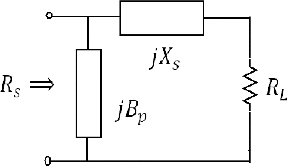
As discussed in the comprehensive network theoretic formulation of the technique by Dutta Roy [Citation10], one could have a parallel development with the L-network having the shunt arm Bp across RL and the series arm Xs in series with the source (this is called network D1 in [Citation10]). As mentioned later in this article, this alternative is important in deriving other alternative equivalent circuits for matching.
2.2 Single Frequency Matching
For matching at a single frequency ω0, one choice is to have an inductor L1 for Xs and a capacitor C2 for Bp, while the other choice is to have C1 for Xs and L2 for Bp. Using the first choice, the element values are: L1 = R1/ω0 and C2 = G2/ω0.
2.3 Application of Frequency Transformation
Frequency transformation is a well-known technique in analog filter design [Citation11] by which a normalized low-pass filter with cut-off at 1 radian/sec can be transformed to any other kind of filter, be it high-pass, band-pass, band-stop, or multiband-pass, with the same tolerances as in the prototype. Basically, it transforms the frequency of 1 radian/sec to the cut-off frequencies of the desired filter. In more general terms, the performance at 1 radian/sec is reproduced in the transformed filter at the desired frequencies. There is no reason why performance cannot be impedance matching, as demonstrated in [Citation9,10] and this article.
Let S denote the complex frequency variable in the single frequency matching network and let ω0 be normalized to 1 radian/sec. Then the problem reduces to that of transforming S = ±j1 to the multiple frequencies s = ±jωk, where, in general, k = 1 … N, s being the complex frequency variable in the transformed network. As is well known [Citation12,13], the transformation function is an LC immittance (impedance or admittance) function of the form(6) where the limits of the summation are determined by the number of frequencies at which matching is required. For example, if N = 2, then the first two terms in Eq. (Equation6
(5) ) suffice. Alternatively, one can use only the first term in the summation, which, in fact, is of the same form as the reciprocal of the first two terms. For N = 3, as is the case in the example to follow, either of the first two terms and one term in the summation serve the purpose. In general, for N odd and ≥3, either of the first two terms is to be taken along with the summation with i ranging from 1 to (N − 1)/2. For N even and ≥4, there are two choices, viz. (1) take the first two terms and the summation with i ranging from 1 to (N − 2)/2 or (2) take only the summation with i ranging from 1 to (N/2). In addition, as already mentioned, there are two choices for the basic single frequency matching network. Clearly, with the flexibility in choosing the basic network and the transformation function, one can generate a number of matching networks having the same performance. Some more alternative networks can be generated by synthesizing each of the reactance and susceptance functions by the other Foster or Cauer or mixed canonic forms. From this multiplicity of networks, one can choose the best one using some appropriate criterion like the total inductance or capacitance or the spread in the values of the components.
3. TRIPLE FREQUENCY MATCHING NETWORK
We shall now illustrate the simplicity, elegance, and flexibility of the frequency transformation technique by designing a triple frequency matching network. The basic network is shown in , where the fact that ω0 has been normalized to 1 radian/sec has been taken into account. One appropriate transformation for this case is(7) The impedance of L1 ( = R1) thus transforms into
(8) The right-hand side of Eq. (Equation8
(7) ) represents a series connection of a capacitance Cse = 1/(k0 R1) and a parallel LsCs circuit with Ls = k1 R1/q1 and Cs = 1/(k1 R1), as shown in .
Similarly, the admittance of C2 ( = G2) transforms to the circuit shown in the shunt arm of with the following element values: Lpe = 1/(k0 G2), Cp = k1 G2/q1, and Lp = 1/(k1 G2).
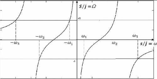
Now the only task that remains to be done is to find the values of k0, k1, and q1. For this purpose, put S = j1 and s = jω in Eq. (Equation8(7) ); after simplification, we get the following equation in ω:
(9) The roots of this equation should give ω1, ω2, and ω3, but not all with positive signs. To find which one(s) would be positive, we sketch the reactance function of Eq. (Equation8
(7) ) as shown in and find the frequencies at which S/j = 1. Clearly, the roots of Eq. (Equation9
(8) ) are −ω1, ω2, and −ω3. also shows that had we taken S/j = −1 in Eq. (Equation8
(7) ), the resulting cubic equation would have the roots ω1, −ω2, and ω3. Returning to Eq. (Equation9
(8) ), we see that the left-hand side should be equal to
(10)
Figure 2: Triple frequency impedance transformer: (a) basic single frequency matching circuit and (b) triple frequency matching circuit with element values given in the text.
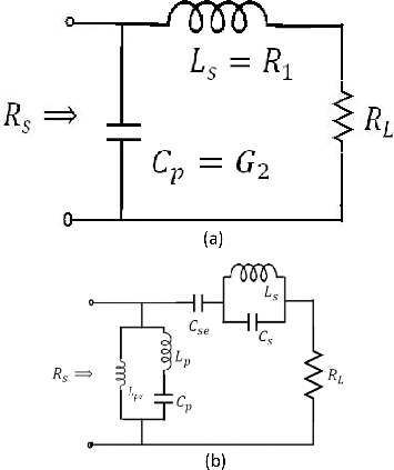
Figure 3: Reactance sketch of Eq. (Equation8(7) ).
4. ALTERNATIVE CIRCUITS FOR TRIPLE FREQUENCY MATCHING
As mentioned in the previous section, several alternative circuits for the triple frequency impedance matching can now be obtained. network, as it is, has the shunt arm in Foster 2 form (henceforth abbreviated as F2) and the series arm in Foster 1 form (henceforth abbreviated as F1). The shunt arm can also be realized in F1 and the series arm can also be realized as F2. Accordingly, we have four alternative circuits, viz. (F2, F1), (F2, F2), (F1, F2), and (F1, F1). Note that for a three-element network, Cauer forms will reduce to either F1 or F2.
Second, using an inductance for Bp and a capacitance for Xs in the basic network of , and then applying the transformation of Eq. (Equation7(6) ), one obtains a different circuit which also allows four different circuits to be generated.
Third, if the basic network is chosen as D1 of [Citation10], in which there is a shunt arm Bp across RL and a series arm Xs in series with RS, then as in the case of D2 discussed so far, another eight networks can be generated, thus making a total of 16 alternative circuits for the same impedance matching purpose.
As mentioned in Section 2.2, an alternative transformation for triple frequency impedance matching is(13) The values of the constants have been worked out in [Citation10] along with a possible circuit by transforming the basic network D1, in which the series arm is F1 and the shunt arm is F2. Following the same procedure as in the case of Eq. (Equation7
(6) ), another 16 different circuits can be generated, thus making a grand total of 32 alternative circuits for any specified triple frequency impedance matching problem.
All these circuits can now be compared in terms of total inductance, total capacitance, maximum inductance, maximum capacitance, inductance spread, and capacitance spread, as done in [Citation10] for a dual frequency impedance matching circuit, and the best one can be chosen in accordance with a predetermined criterion.
5. CONCLUSIONS
As discussed and demonstrated in this article, application of frequency transformation on the basic single frequency impedance matching network eases the problem of designing multiple frequency matching networks. It gives multiple solutions and facilitates the choice of the most suitable network in a given situation.
ACKNOWLEDGEMENTS
This work was supported by the Indian National Science Academy through the Honorary Scientist scheme. The author thanks Shoubhik Dutta Roy and Yashwant V Joshi for their help in the preparation of this article. Thanks are also due to the reviewer for constructive comments.
Additional information
Notes on contributors
S.C. Dutta Roy
S.C. Dutta Roy received his Bachelor's, Master's, and Doctorate degrees from the University of Calcutta, Calcutta, India, in 1956, 1959, and 1965, respectively. He was a lecturer at the University of Kalyani, West Bengal, India, for five years before taking up an assistant professor's position at the University of Minnesota, Minneapolis, Minnesota, USA. He returned to India in 1968 and spent more than four decades at the Indian Institute of Technology Delhi (IITD) as an associate professor, professor, head of the department, and dean of undergraduate studies. On sabbatical leave from IITD, he spent a year at the University of Leeds, UK, and another year at the Iowa State University, Ames, Iowa, USA, as a visiting professor. Upon superannuation from IITD, he continued there first as an emeritus fellow, then as a senior scientist of the Indian National Science Academy (INSA), and finally as an honorary scientist of the INSA. Currently, he continues working from home as an INSA honorary scientist.
Professor Dutta Roy's research interests are in circuits, systems, and signal processing. He has published more than 260 research papers in IEEE, IEE, and other reputed journals and transactions, and has mentored 30 PhD students. He holds one US and three Indian patents and is the creator of five highly popular full-length video courses, four of which are available on YouTube for free downloading. His research has been recognized by a fellowship of the IEEE and of all the National Academies of Science and Engineering of India, and a distinguished fellowship of the Institution of Electronics and Telecommunication Engineers, New Delhi, India, and several national awards, including the most prestigious Shanti Swarup Bhatnagar Prize.
E-mail: [email protected]
REFERENCES
- C. Monzon, “A small dual frequency transformer in two sections,” IEEE Trans. Microw. Theory Tech., Vol. 51, no. 4, pp. 1157–61, Apr. 2003.
- Y. Wu, Y. Liu, and S. Li, “A dual frequency transformer for complex impedances with two unequal sections,” IEEE Microw. Wirel. Compon. Lett., Vol. 19, no. 2, pp. 77–9, Feb. 2009.
- X. Liu, Y. Liu, S. Li, F. Wu, and Y. Wu, “A three section dual band transformer for frequency dependent complex load impedance,” IEEE Microw. Wirel. Compon. Lett., Vol. 19, no. 10, pp. 611–3, Oct. 2009.
- F. Paredes, G. Gonzales, J. Bonache, and F. Martin, “Dual band impedance matching networks based on split-ring resonators for application in RF identification (RFID),” IEEE Trans. Microw. Theory Tech., Vol. 58, no. 5, pp. 1159–66, May 2010.
- M.-L. Chuang, “Dual band impedance transformer using two-section shunt stubs,” IEEE Trans. Microw. Theory Tech., Vol. 58, no. 5, pp. 1257–63, May 2010.
- C.-S. Lee, and C.-L Yang, “A coupling matrix based design of triple band matching network,” IEEE Microw. Wirel. Compon. Lett., Vol. 23, no. 8, pp. 391–3, Aug. 2013.
- Y. Liu, Y. J. Hao, and Y. Hao, “Lumped dual frequency transformer for frequency dependent complex loads,” Prog. Electromagn. Res., Vol. 126, pp. 121–38, 2012.
- Y. Liu, Y. Chen, and Y. J. Zhao, “Lumped triple-frequency impedance transformer,” Electron. Lett., Vol. 48, no. 19, pp. 1193–4, Sep. 2012.
- N. Nallam, and S. Chatterjee, “Multi-band frequency transformations, matching networks and amplifiers,” IEEE Trans. Circuits Syst.-I: Regular Papers., Vol. 60, no. 6, pp. 1635–47, Jun. 2013.
- S. C. Dutta Roy, “Network design for multiple frequency impedance matching by the frequency transformation technique,” IETE J. Res., Vol. 59, no. 6, pp. 698–703, Nov. to Dec. 2013.
- S. C. Dutta Roy, “On the design of a multiple pass-band filter by frequency transformation,” IETE J. Res., Vol. 58, no. 1, pp. 20–3, Jan. 2012.
- L. Wienberg, Network Analysis and Synthesis, Hoboken, NJ: Wiley, 1962.
- E. A. Guillemin, Synthesis of Passive Networks, Hoboken, NJ: Wiley, 1964.