
 ?Mathematical formulae have been encoded as MathML and are displayed in this HTML version using MathJax in order to improve their display. Uncheck the box to turn MathJax off. This feature requires Javascript. Click on a formula to zoom.
Abstract
Measurements of DC electric conductivities of four types of silicone rubber-based polymers for use in high voltage insulation systems of power components are reported. The field dependences of the conductivities obtained by two different techniques, namely by utilizing steady-state currents through materials’ samples placed between metallic electrodes and by employing surface potential decay characteristics in an open circuit configuration, are compared and discussed. It is shown that the surface potential decay technique allows for a wider range of electric field strength and reduces the time span of the measurements.
Introduction
Silicone rubber (SIR) based elastomers doped with various fillers are widely employed in power technology and electronics. An example is high-temperature vulcanized (HTV) rubber containing aluminum trihydrate (ATH), which is utilized for high-voltage (HV) insulation purposes in power components due to its low electric conductivity, lower weight as compared to traditionally used glass and porcelain, mechanical stability and other properties, which are essential for specific applications (e.g. hydrophobicity for outdoor HV insulation systems). Since the electric conductivity is the main characteristic of SIR defining its insulating performance, an accurate determination of this quantity in a wide range of electric fields is crucial from the point of view of HV insulation design and necessity of controlling charge accumulation and distribution in/on it. The latter is of special importance for high-voltage direct current (HVDC) applications,[Citation1,Citation2] where the amount of accumulated charges can be high enough to cause undesirable modifications of the electric field and thus alter the performance of the insulation systems.
Measurements of volumetric electric conductivity are standardized.[Citation3,Citation4] They are typically conducted using flat material samples placed between metallic electrodes (an example is shown in ) and the conductivity values are deduced as a ratio between the measured current density and the applied electric field. Despite this simplicity, the implementation of such measurements on highly resistive materials is not straightforward due to several reasons. In particular, to obtain true DC conductivity, a steady state magnitude of the current density should be reached that may require very long measuring time[Citation5] or may be even not achievable.[Citation6] There are also other factors affecting the results of the measurements such as the strength of the applied electric field, temperature, conditions on electrode-material interfaces, etc.[Citation7–11] The latter defines charges (and respectively currents) injected into the material during the measurements, which introduce uncertainties in the measured results (especially at high test voltages) and impose limits for the applied test field magnitude.
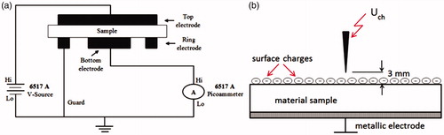
Figure 1. Schematic illustrations of the electrodes arrangements for bulk current measurements (a) and for corona charging of the material sample (b).
The influence of the electrodes can in principle be avoided by using non-contact techniques. An attempt of implementing such a procedure was undertaken in,[Citation12] where the volume resistivity of epoxy resin was deduced from surface potential decay (SPD) characteristics. The latter was obtained by charging an open surface of a flat material sample resting on a grounded metallic plate by corona discharge () and recording time variations of the induced surface potential after switching off the corona source. The SPD measurements in[Citation12] were implemented utilizing a non-contact method.[Citation13] The main distinction of this procedure from the standard technique is that one of the metal-material interfaces is replaced by a virtual electrode created by electric charges deposited on the open surface of the sample as shown schematically in . With time, the voltage applied across the sample (and thus the electric field strength in it) decreases due to SPD process that is in contrast to the standard method where the test voltage is fixed. This natural decrease of the electric field in the material due to SPD may in principle allow for obtaining information about field dependence of its conductivity from a single measured SPD characteristic whereas the current-based method yields just a single value of the conductivity for the given applied field. This may potentially speed-up the measurement procedure and needs to be further investigated.
In the present article, field dependencies of electric conductivities of four types of SIR intended for use in HVDC insulation systems are determined by utilizing both volumetric currents and SPD characteristics. The results obtained by the two methods are compared in order to validate the SPD-based technique and to reveal its possible advantages.
The experiment
Setup and procedure for obtaining material conductivity from measured currents
The measurements were realized according to.[Citation4] In the experiments, a material sample was placed in the resistivity test fixture Keithley 8009, which is a three-electrode test cell as shown in . The test fixture was connected to Keithley 6517 A electrometer equipped with an internal test voltage source. A procedure based on the stepwise increase of the DC test voltage was utilized. The tests started by applying the voltage of 300 V across the sample and measuring the response current, which consisted of a spike of a capacitive current followed by decaying polarization current. After achieving a quasi-steady state, the test voltage was increased to 600 V and the procedure was repeated. The following steps included the measurements at the test voltage of 800 V, 900 V, and 1 kV. The field dependent conductivities of the materials were deduced from the respective steady-state currents. The experiments were conducted at ambient room conditions (temperature 22 °C and relative humidity 50–60%). The measurement was repeated at least three times for each material in order to check the repeatability of the results. Between the consecutive measurements, the samples were short-circuited and grounded for a long time to discharge.
Setup and procedure for SPD measurements
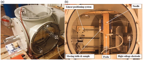
The arrangement used for obtaining surface potential decay characteristics for the materials was mounted inside a sealed metallic chamber with an internal volume of ∼1 m3. The photographs of the setup are shown in . It contained a corona charging system for depositing charges on the surface of a material sample, which resulted in certain surface potential distribution. After charging, the latter was monitored using a Kelvin-type vibrating probe (Trek 3455ET) connected to an electrostatic voltmeter (Trek 341B, measured range ±20 kV). The SPD measurements were conducted using the following procedure. Firstly, the surface of a sample was exposed to negative corona discharge from a needle electrode for 2 minutes at ambient pressure(the needle tip radius was 125 µm, the distance between the tip and the sample was ∼2 mm). After that, the air pressure inside the test vessel was reduced to 3 × 10⁴ ± 103 Pa (300 ± 10 mbar) to prevent possible neutralization of the deposited charges by free ions in the air and the distribution of the induced surface potential VS was recorded by scanning the sample surface with the probe. The scan was repeated at different times after charging to obtain a set of distributions. The SPD characteristics for further analyses were determined by utilizing the time variation of VS at fixed location on the sample. The experiments were conducted under laboratory conditions (air temperature ∼22 °C, humidity ∼50%).
Figure 2. General (a) and top (b) views of the experimental setup. In (b), sample positioning system is shown with charging and scanning setups mounted inside the test vessel. Material sample is placed on the top of plate. Note that the charging needle and the probe are beneath the arm and are facing downwards to the sample.
Material samples
In the present study, flat samples of four types of HTV silicone rubber were used. The materials were based on poly-di-methyl-siloxane reinforced with silica fillers and doped with additives introduced to meet the requirements of diverse HV applications. Specifications of the materials are provided in . Observe that material B is the same as material A with the extra addition of ATH filler and the same is valid for materials C and D. The dimensions of the samples were 100 × 100 × L mm3, where thickness L is the average of four readings obtained at various distances from the sample edge. The measured dielectric constantsand surface conductivities KS of the materials are listed in (the former were measured using IDAX300 insulation diagnostic system). As seen, the surface conductivities are extremely low, making surface leakage of deposited charges negligible. Taking into account that neutralization of surface charges due to air ions is negligible at the reduced pressure in the test vessel during the experiments, it can be argued that the SPD process under conditions of the present study is dominated by bulk conduction through the material.
Table 1. Specification of the studied materials.
Table 2. Surface conductivities (at 1 kV), dielectric constants εr(at 50 Hz) and thickness of the samples.
Results and discussion
Volume currents
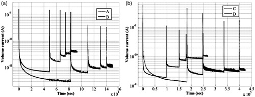
Time variations of the currents recorded during standard measurements as described in Section “Setup and procedure for obtaining material conductivity from measured currents” are shown in . As seen, times required for the volume currents to reach steady state values are different for the studied SIRs and are strongly influenced by material composition and electric field strength. Thus after applying the first voltage step, times to steady state are ∼14 h and ∼28 h respectively for ATH filled rubbers B and D whereas they are ∼22 h and ∼50 h for corresponding counterparts A and C (without additional fillers). Hence, doping by ATH leads to faster relaxation of the volume current that may be attributed to the possible formation of conductive paths along interfacial layers between filler particles and base material.[Citation14] It is important to mention here that the currents at the instants mentioned above are essentially at quasi steady-state and still slightly vary, reflecting processes of slow polarization in the bulk. To determine actual conduction currents, much longer time span is required. Thus, the longest measuring time used for material C in one of the experiments was ∼116 h (∼5 days) and even such long-lasting measurement did not allow for completely mitigating the polarization effects.
As mentioned above, the experimental procedure described in Section “Setup and procedure for obtaining material conductivity from measured currents” may also cause injection of charges and space charge accumulation in the material due to the sequential application of increasing test voltages.[Citation7,Citation15] To identify the existence of space charge effect, dependencies of the current density J(A/m2) on the applied field E(V/m) can be plotted in log-log coordinates and fitted by a straight line. According to the theory of space charge limited currents,[Citation16,Citation17] any increase of the slope of this line above unity (corresponding to pure Ohmic behavior) reflects space charge accumulation in the material. Following this approach, the J(E) characteristics obtained by utilizing the quasi steady-state currents from are plotted in . As can be seen, data for materials A and C are best fitted by lines with slopes nearly equal to 1. However for ATH filled materials B and D, the data points deviate from the linear fit at higher fields, indicating the existence of a threshold, above which a possibility for charge injection and accumulation may arise. At the highest field level, the current magnitudes exceed those expected from Ohmic conduction in approximately two times. Considering such deviations insignificant, one may assume that space charge effect is negligible in the unfilled materials as well as in the materials doped with ATH at low fields and thus the conduction is of Ohmic type under these conditions.
Figure 3. Measured volume currents at room temperature for materials A, B (a) and C, D (b) at different amplitudes of test voltages. The first spike in both the figures corresponds to the application of 300 V, followed by 600, 800, 900, and 1 kV.
The values of the volume conductivities KV (S/m) and standard deviations obtained using the quasi steady-state currents from and data in , respectively, are provided in for different test voltages. As seen, the deviations from the mean values are rather weak indicating good repeatability of the measurements. The conductivities of rubbers A and C are pretty constant whereas the values of KV increase with the field (i.e. test voltage) for ATH doped SIRs, and material D appears to be the most conductive. In general, the field dependences are rather weak and the variations of the values of KV are less than two times.
Figure 4. Current density J vs. applied electric field E characteristics for studied materials. The solid and broken lines represent liner fittings with slope 1, the error bars show the standard deviations.
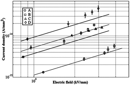
Table 3. Bulk conductivities of the studied materials deduced from the measured volume currents at different amplitudes of DC test voltages.
Surface potential decay
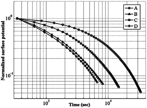
Normalized SPD characteristics measured on studied materials are shown in . The data represent the average of three measurements conducted under similar conditions and the discrepancies in the results were below 10%.[Citation6] It can be noticed from the figure that the different material compositions and thus the bulk properties play a deterministic role in the decay process. For materials containing an additional amount of ATH filler (B and D), the characteristics are similar. However, the SPD on original SIRs (A and C) is very different that can be attributed to the differences in their properties caused by the various types of used curing agents. It is evident also that the time required for the neutralization of deposited surface charges can be correlated with the volume conductivities of the materials (). Thus the decay is the fastest for material D, which is characterized by the highest conductivity among the studied materials. At the same time, the lower conductivity of material A (by almost one order of magnitude) yields much longer time for surface potential to vanish. Quantitatively, the time needed for surface potential to decay to 50% of its initial value is approximately 2 times longer for material C and more than 5 times longer for material A than that for material D. These observations confirm that it is the intrinsic conduction that mainly controls surface potential/charge decay in the reported study.
Figure 5. Normalized surface potential decay characteristics obtained at room temperature for different samples of HTV silicone rubber materials.
Evaluation of bulk conductivities from SPD characteristics
Since the decay of the deposited surface charge in the experiments is solely controlled by the volume currents (ion neutralization and surface leakage are negligible), the rate of change of its density (C/m2) can be expressed as
(1)
(1)
At the same time, by applying Gauss’s law and accounting for the fact that the field between the probe and the sample surface is zero during the measurements (that is the working principle of the Kelvin probe used), the surface charge decay rate can be defined as[Citation18]
(2)
(2)
where
is the permittivity of vacuum. Combining EquationEquations (1)
(1)
(1) and Equation(2)
(2)
(2) , the relation between the material’s bulk conductivity and SPD rate can be obtained as[Citation19]
(3)
(3)
Following (3), data presented in were numerically differentiated with respect to time and the results were multiplied by the permittivity values presented in . The obtained field dependences of KV are shown in (together with the results of the standard measurements for comparison purposes). It is notable that the dependences KV(E) for the unfilled silicone rubbers A and C are quite different, following the behavior of the surface potentials in . For these materials, the increase of the conductivity with the field at high field magnitudes is even stronger than exponential, especially for SIR A which is the most resistive. In contrast, the conductivities of ATH-filled rubbers B and D are higher than that of pure materials and are practically equal at the field strength exceeding 2 kV/mm. This can be attributed to the dominant effect of the ATH filler. One should note however that the observed variations take place in rather narrow interval (within two orders of magnitude), i.e. the influence of the field on the conductivities of the studied HTV silicone rubbers is rather weak.
Figure 6. Bulk conductivities of the materials deduced from the measured surface potentials (solid symbols) and obtained from standard measurements (SM) of volume currents. Error bars for SPD are not displayed due to a very weak scatter between the measurements [Citation6].
![Figure 6. Bulk conductivities of the materials deduced from the measured surface potentials (solid symbols) and obtained from standard measurements (SM) of volume currents. Error bars for SPD are not displayed due to a very weak scatter between the measurements [Citation6].](/cms/asset/701a358a-0c38-499d-a71d-9f887494416a/gpac_a_1516369_f0006_b.jpg)
Comparison of the methods
From the results in , it can be noticed that the SPD measurements provide conductivity values of the same order of magnitude as the output from the standard measurements. The percentage deviations () calculated with respect to the data received from the conventional method are within the range of except for material B for which they are higher. Such deviations are quite common in practice and are close to uncertainties typical for measurements of the conductivity of highly resistive materials. Taking this into account the fact that the data deduced from the volumetric currents cannot be considered as a true reference due to the reasons discussed in Section “Volume currents”, the results in and suggest that SPD can be seen as an alternative method for determining the electric conductivity of insulating polymers. One should mention that the total measuring time needed for characterization of the studied materials utilizing SPD technique is significantly shorter (few hours) than the time required for measurements by the standard method (may be up to few days). Furthermore, it was noticed while conducting the SPD measurements that the corona charging provided maximum magnitudes of the surface potentials up to 5–6 kV, depending upon material type. Such magnitudes of VS are much higher than the maximum DC test voltage of 1 kV applied during conventional measurements to induce measurable volume currents through the materials. In principle, the latter can be increased provided that discharges from the metallic electrodes in the air are prevented, e.g. by immersing the test cell into insulating oil that, however, makes the realization of the setup rather complicated. In this respect, the SPD based method seems to be more flexible in establishing voltage (field) levels during testing, which change with time in a natural way being controlled by the conductive properties of the material and provide this way conductivity values at various fields strengths. The actual range of E is defined by the maximum of VS after charging and its minimum value corresponding to the time at which the SPD measurement is completed. Thus, as seen from , the data provided by the SPD technique are in the range of E which spans over one decade and is much wider than that provided by the standard method.
Table 4. Deviations of the values KV obtained from SPD characteristics from the output of standard measurements.
Conclusions
Field dependences of electrical conductivities of HTV silicone rubbers intended for use in various HVDC applications have been obtained utilizing measured volumetric currents and SPD characteristics. The results indicated the influences of the curing agent used in the manufacturing process and the presence of ATH filler on the measured conductivity values. It is demonstrated that both measuring methods yielded comparable results and the SPD based technique allows for a significant reduction of the measuring time and a wider range of the applied electric field compared to the standard technique utilizing volumetric currents.
References
- Lutz, B., and J. Kindersberger. 2011. Surface charge accumulation on cylindrical polymeric model insulators in air: simulation and measurement. IEEE Trans. Dielect. Electr. Insul. 18:2040–2048.
- Reddy, C. C. 2012. Conduction and space charges in polymeric dielectrics and nanocomposites. Proceedings of IEEE 7th International Conference on Industrial and Information Systems (ICIIS 2012), Chennai, India, August 2012.1-4.
- International standard IEC 62631-3-1. 2016. Dielectric and resistive properties of solid insulating materials – Part 3-1: Determination of resistive properties (DC methods) – Volume resistance and volume resistivity – General method, IEC.
- ASTM D257-14 2014. Standard Test Methods for dc Resistance or Conductance of Insulating Materials. West Conshohocken, PA: ASTM International.
- Tsekmes, I. A. 2012. Electrical characterization of polymeric DC mini-cables by means of space charge & conduction current measurements. PhD Thesis, Delft University of Technology, Delft, Netherlands.
- Alam, S. 2014. Surface charge dynamics on polymeric insulating materials for high voltage applications. Technical Licentiate Thesis, Chalmers University of Technology, Gothenburg, Sweden.
- Raju, G. G. 2003. Dielectrics in Electrical Fields. New York: Dekker, Inc.
- Rakowska, A., and K. Hajdrowski. 2000. Influence of different test conditions on volume resistivity of polymeric insulated cables and polyethylene samples. Int. Conf. Diel. Mat. Meas. Appl., Edinburgh. 281–284.
- Olsson, C. O. 2008. Modelling of thermal behavior of polymer insulation at high electric dc field. 5th European Thermal Sciences Conference, The Netherlands.
- Nelson, J. K. 2010. Dielectric Polymer Nanocomposites. New York: Springer.
- Viertel, J., L. Petersson, A. Friberg, G. Dominguez, and C. Törnkvist. 2013. Electrode influence on dc conductivity measurements of low density polyethylene. IEEE Int. Conf. Solid Diel., Bologna. 1048–1051.
- Lutz, B., and J. Kindersberger. 2009. Determination of volume resistivity of polymeric insulators by surface charge decay. Proceedings of the International Symposium on high voltage engineering, Johannesburg, South Africa, pp. 28–33.
- Noras, M. A. 2002. Non-contact surface charge/voltage measurements fieldmeter and voltmeter methods. Trek Application Note, number 3002, Trek Inc., New York.
- Yamanaka, S., T. Fukuda, G. Sawa, M. Ieda, M. Ito, and T. Seguchi. 1995. Effect of filler concentration on electrical conductivity and ultralow-frequency dielectric properties. IEEE Trans. Dielect. Electr. Insul. 2:54–61.
- Teyssedre, G., and C. Laurent. 2005. Charge transport modeling in insulating polymers: from molecular to macroscopic. IEEE Trans. Dielect. Electr. Insul. 12:857–875.
- Lampert, M. A. 1956. Simplified theory of space charge limited currents in an insulator with traps. Phys. Rev. 103:1648–1656.
- Auge, J. L., C. Laurent, D. Fabiani, and G. C. Montanari. 2000. Investigating dc polyethylene threshold by space charge. Current and electroluminescence measurements. IEEE Trans. Dielect. Electr. Insul. 7:797–803.
- Min, D., M. Cho, A. R. Khan, and S. Li. 2012. Surface and volume charge transport properties of polyimide revealed by surface potential decay with genetic algorithm. IEEE Trans. Diel. Elec. Insul 19:600–608.
- Molinie, P. 2005. Measuring and modeling transient insulator response to charging: the contribution of surface potential studies. IEEE Trans. Dielect. Electr. Insul. 12:939–950.