
 ?Mathematical formulae have been encoded as MathML and are displayed in this HTML version using MathJax in order to improve their display. Uncheck the box to turn MathJax off. This feature requires Javascript. Click on a formula to zoom.
Abstract
TDI CMOS image sensors are the most widely used photodetectors in space earth observation and multispectral imaging. The displacement damage caused by high-energy proton irradiation in the space environment leads to the continuous degradation of TDI CMOS image sensor parameters, seriously affecting its performance, reliability, and service life. This paper focuses on a space-based TDI CMOS image sensor chip and carries out 3 MeV proton irradiation tests and post-irradiation annealing tests to obtain the change rules of optical and electrical parameters. The degradation mechanism of sensitive parameters of TDI CMOS image sensors caused by proton irradiation is analyzed, and the sensitive region of proton displacement damage are discussed. The study demonstrates that after proton irradiation, the parameters especially full well capacity and temporal dark noise of the device degrade less, with small sensitivity to proton irradiation. However, the dark current, CTE, and pixel column FPN significantly degrade, and the degree of degradation is linearly related to the proton irradiation dose. In addition, the test also obtained the short-term and long-term annealing changes of sensitive parameters after proton irradiation of TDI CMOS image sensors, providing scientific advice for TDI CMOS image sensors space proton radiation effect tests and evaluations. The research results of this paper provide important references for the evaluation of radiation effects, on-orbit performance estimation, and radiation resistance reinforcement of space-based TDI CMOS image sensors.
1. Introduction
CMOS Image Sensors (CIS) are the most widely used optical detectors in space earth observation and space scientific exploration. They are divided into two types based on the pixel arrangement: area array type and linear array type. The linear array type CIS exposes the object in each row of pixels in a scanning manner and synthesizes a complete image from the exposure results of multiple rows. Its main advantage over the area array CIS is high frame rate readout and multispectral imaging (Citation1). However, the smaller integration time means the smaller signal level, resulting in a significant reduction in the signal-to-noise ratio (SNR) of the CIS. The SNR reduction is more pronounced in low-light environments (Citation2).
Time Delay Integration (TDI) CMOS Image Sensors effectively improve the SNR of linear array CMOS Image Sensors by exposing multiple rows simultaneously and accumulating signals, without affecting the frame rate (Citation3). Therefore, they have extremely important application merit in major scientific and technological fields especially space earth observation and multispectral imaging (Citation4–6).
Various high-energy particles, such as protons, exist in the satellite orbital space environment (Citation7, Citation8). The displacement damage effect caused by proton irradiation leads to severe degradation of CIS parameters (Citation9, Citation10). In the past two decades, a significant amount of research has been conducted on the proton radiation effects of TDI CIS. Joseph E. Rushton et al. evaluated the proton irradiation effects on a TDI CIS based on the E2 V technology (Citation11). The experimental results show that high-energy protons with an equivalent 10 MeV proton fluence of 5 × 10⁹ p/cm2 and 1 × 10¹⁰ p/cm2 have a minimal impact on charge transfer inefficiency (CTI). However, after proton irradiation with an equivalent 10 MeV proton fluence of 1 × 10¹⁰ p/cm2, the dark current of the device increases by 10% to 15%. Moreover, the degradation of the dark current becomes more severe as the proton irradiation dose increases. Jérôme Pratlong et al. conducted proton irradiation experiments on the Teledyne charge domain accumulation type TDI CIS-125 (Citation12). It is shown that both the dark current and the charge transfer efficiency (CTE) exhibit significant degradation after irradiation, and the degradation becomes more serious with the increase of proton irradiation fluence.
Some literature has reported on the changes in dark current and CTE after proton irradiation of TDI CIS, but the mechanism of displacement damage defects caused by irradiation and the degradation mechanisms of parameters such as CTE and dark current are not clear. In addition, the effects of other important parameters of TDI CIS such as full well capacity, temporal dark noise, pixel column fixed pattern noise (FPN), and post-irradiation annealing on the parameters have not been reported. There is a lack of systematic research on the proton irradiation effects of TDI CIS, which cannot provide basic support for radiation effect evaluation and radiation resistance reinforcement. This paper conducts experiments from both proton irradiation and post-irradiation room temperature annealing of TDI CIS, focusing on the basic mechanism of proton displacement damage. A systematic discussion is presented on the degradation rules and damage mechanisms of TDI CIS light field parameters (including full well capacity and CTE) and dark field parameters (including dark current, temporal dark noise, and pixel column FPN) caused by proton irradiation. The sensitive region of proton displacement damage are analyzed on the basis of irradiation and annealing, providing important references for radiation effect evaluation, on-orbit performance prediction, and radiation resistance reinforcement of TDI CIS for space applications.
2. Samples and test methods
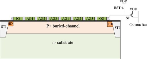
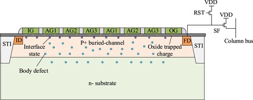
Figure shows the pixel structure of the TDI CIS device. They are separately injection gate (IG), transmission gates (AG1∼AG3), injection drain (ID), output gate (OG), floating diffusion region (FD). During the normal operation of the device, the signal charge packet is injected and sequentially transmitted between the potential wells. After being transferred to the output gate, the signal is finally amplified and read out through the source-follower (SF) transistor.
Figure 1. Schematic diagram of the TDI CIS pixel structure.
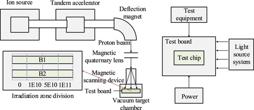
Proton irradiation tests were carried out on the 2 × 6 MeV EN serial electrostatic accelerator at the Institute of Heavy Ion Physics, Peking University. Figure shows the schematic diagram of the irradiation and testing equipment. The proton energy is 3 MeV, and the irradiation dose rate is 5 × 10⁷ p/(cm2·s). Shift tests are performed at cumulative doses of 1 × 10¹⁰ p/cm2, 5 × 10¹⁰ p/cm2, and 1 × 10¹¹ p/cm2, respectively. During the proton irradiation test, all pins are connected together and grounded. The post-irradiation annealing test is carried out at room temperature (25°C), with a room temperature annealing time of 21 days. During the room temperature annealing, the device parameters (full well capacity, CTE, dark current, temporal dark noise, and column FPN) are tested multiple times.
Figure 2. Schematic diagram of the irradiation and testing equipment.
3. Results and discussion
The discussion mainly focuses on two aspects: light field parameters and dark field parameters. Among the light field parameters, the main ones include full well capacity and CTE, while the dark field parameters include dark current, temporal dark noise and column FPN.
3.1. Light field parameters
The full well capacity is an important indicator for the evaluation of CMOS image sensor characteristics and is also one of the sensitive parameters for displacement damage. It represents the maximum number of electrons that can be accommodated by the potential well, with the unit being ke-. The full well capacity can be directly reflected in the light response curve, as shown in Figure .
Figure 3. Variation of gray value of 3 MeV proton light response with the change of integration level.
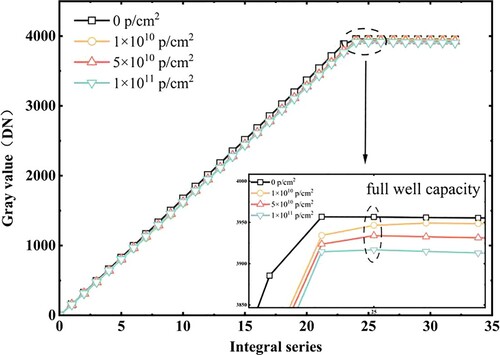
Figure shows the variation of the full well capacity with respect to the irradiation dose and annealing time. After 3 MeV proton irradiation, both the gray value of the light response and the full well capacity decrease. However, the overall degradation is small, with a total degradation ratio of about 5%, indicating that the full well capacity is not a sensitive parameter for proton displacement damage. As shown in Figure , proton irradiation introduces oxide traps and interface traps in the gate oxide layer and generates bulk defects in the depletion layer and the underlying bulk Silicon in the buried trench (Citation13). For the subsequent annealing, it can be seen that the full well capacity recovers significantly in the first 3 days, reaching about 50% of the pre-irradiation level. The effect of proton irradiation on the full well capacity is primarily due to ionizing radiation effects. At room temperature, it is mainly the annealing of the oxide trap charge, and only a small amount of displacement damage-induced unstable defects undergo recombination (Citation14).
Figure 4. Variation of the full well capacity of 3 MeV protons with irradiation dose and annealing time.
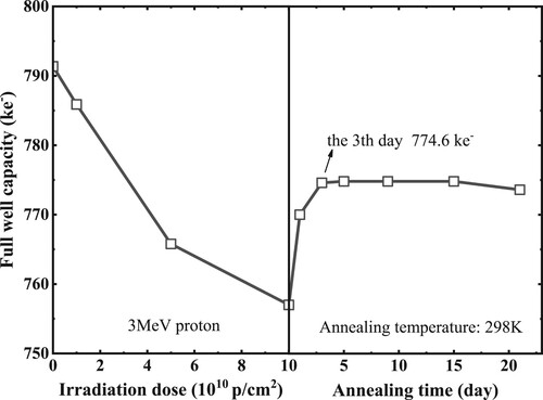
Figure 5. Distribution of interface states and defects introduced by proton irradiation.
CTE represents the charge loss rate from one pixel to the next during charge transport. For CCDs, CTE is the most sensitive parameter to displacement damage (Citation15). TDI CIS is essentially a CCD-on-CMOS structure device, which integrates the CCD structure into the device using standard CMOS process. For TDI CIS, the parameter CTE is also quite sensitive to proton irradiation. In TDI CIS, CTE can be calculated in the following way:
(1)
(1) Where the number of transfer times refers to the number of pixel transfer gratings. The tail signal is the sum of the gray values of all dark rows under the dark field conditions. The lowest order tail signal is the sum of the gray values of all dark rows under the lowest order. The total signal is the difference between the total gray value of the bright rows in the light field and the total gray value of the bright rows in the dark field.
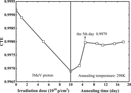
Figure shows the variation of CTE with respect to the irradiation dose and annealing time. Overall, 3 MeV protons cause the decrease of CTE, with a linearly decreasing trend. From the perspective of CTI, we found that the CTI ratio reached 273.5% after proton irradiation. High-energy protons incident collide with lattice atoms in the CCD-like structure, producing a large number of vacancy-interstitial atom pairs to form bulk defects (Citation16). These defects continuously emit charge carriers and simultaneously capture signal charges that are being transferred in the trenches, thereby affecting CTE. Furthermore, only a portion of the captured carriers will be re-emitted by the deep energy levels generated by the defects (Citation17). In the transmission channel of the CCD-like structure, the number of electrons captured by bulk defects is given by Equation Equation2(2)
(2) :
(2)
(2) Where τc and τe are the capture and emission time constants, respectively, and Nt is the density of bulk defects introduced by proton irradiation. Moreover, as the proton irradiation dose increases, the density of the generated bulk defects grows accordingly. The number of electrons captured at the corresponding defect energy levels increases, leading to a decrease in CTE. There is a significant recovery in CTE during the first 5 days before annealing, and after the fifth day, the CTE curve basically remains flat. After the annealing process is completed, the recovery ratio of CTE at 3 MeV is 48.6%. Combined with the degradation ratio after irradiation, it is indicated that interface states and transfer channel displacement damage defects are the main reasons for degradation. During the room temperature annealing process, some of the electrons captured by the interface traps and body defect energy levels are gradually emitted, leading to a slow recovery of CTE.
Figure 6. Variation of CTE with irradiation dose and annealing time.
3.2. Dark field parameters
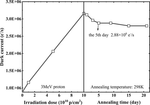
In addition to electrons generated by illumination, CIS can also produce electron–hole pairs due to thermal excitation in the absence of light. This is known as dark current, and the unit is e-/s. The main sources of dark current include interface current generated by buried trenches, depletion region current, diffusion current in the body neutral region, and gate oxide interface state leakage current (Citation18). Dark current is one of the main factors affecting the performance of image sensors and is also a sensitive parameter for spatial proton radiation damage. Figure shows the significant degradation of dark current after proton irradiation. As the irradiation dose increases, the corresponding dark current increases approximately linearly. Proton irradiation produces a large number of displacement damage defects in the body region of the buried trenches inside the image sensor, most of which are distributed in the depletion region and the neutral region. In the depletion region, the defect levels can act as generation-recombination centers for carriers. According to the Shockley-Read-Hall (SHR) theory, the net generation rate of carriers is given by Equation 3.
(3)
(3) Where σn and σp are the capture cross sections of electrons and holes, vth is the velocity of the thermal motion of carriers, p and n are the concentrations of holes and electrons, Ei is intrinsic Fermi level, Nt is defect density, Et is defect level, k is Boltzmann constant, and T is Kelvin temperature. With the increasing number of displacement damage defects in the depletion region, the carrier generation rate increases linearly. Furthermore, the closer the defect energy level is to the bandgap center, the higher the carrier generation rate (Citation19). It can be seen that the recovery of dark current is mainly reflected in the first 5 days of annealing, and afterwards, it basically remains stable and does not change with the annealing time. After the annealing process is completed, the recovery ratio of 3 MeV dark current is 15.8%. In room temperature annealing, the recovered portion is mainly due to the annealing of interface states and isolated defects, indicating that both interface states and depletion region shift damage defects are the main sources of dark current after proton irradiation.
Figure 7. Variation of dark current with irradiation dose and annealing time.
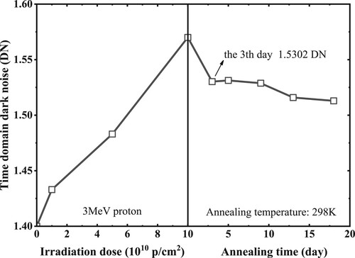
Temporal dark noise, also known as dark noise or readout noise, refers to the dark field noise value obtained by an image sensor in a completely dark environment and under the shortest exposure time condition (in units of DN). Under the condition of the shortest time between no illumination and exposure, the temporal dark noise of TDI CIS can be obtained by calculating the average temporal standard deviation of the gray values in the corresponding image.
(4)
(4) Figure shows the variation of temporal dark noise with changes in proton irradiation dose and annealing time. It can be seen that the temporal dark noise degrades with the increase of the irradiation dose, and the degree of change is approximately linearly related to the irradiation dose. However, the degradation is small, with an overall increase ratio of 12.1%. Proton irradiation produces new defects and interface states in the TDI CIS channel and substrate. With the increase of the incident proton dose, more interface states and defects are introduced, thereby further increasing the temporal dark noise. The temporal dark noise reaches a low value around the third day of annealing, and afterwards the curve tends to stabilize. After the annealing process is completed, the recovery ratio of 3 MeV proton temporal dark noise is 33.6%, indicating that room temperature annealing can only reduce the density of some isolated defects.
Figure 8. Variation of temporal dark noise with irradiation dose and annealing time.
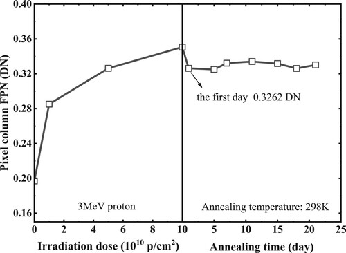
Pixel column FPN is also an important parameter indicator for the performance of TDI CIS. For the pixel column FPN of image sensors, there will be certain non-uniformities in the pixel due to the imperfection of the process. In addition, the non-uniformity of the noise in the readout circuit will also affect the pixel column FPN. As can be seen from Figure , the column FPN of the pixel gradually increases with the increase of proton radiation dose. Moreover, it approaches a linear increase after 1 × 10¹⁰ p/cm2 dose, which indicates that the impact of radiation dose on the readout circuit noise gradually increases. The possible reason is that as the charge packet transmits through the channel, the defect levels introduced by bulk defects increase, making the capture and emission processes of carriers more frequent. On the first day of annealing, the recovery ratio of pixel column FPN is relatively large, and it almost doesn't change afterwards. Throughout the annealing process, the annealing ratio of pixel column FPN is less than 20%. This indicates that only a portion of the body defect energy levels that affect the readout circuit noise have occurred recovery, and the readout circuit noise is not sensitive to room temperature annealing.
Figure 9. Variation of proton pixel column FPN with irradiation dose and annealing time.
3.3. Analysis of displacement damage sensitive regions
In the previous sections, we discussed the effects of 3 MeV protons on the full well capacity, CTE, dark current, temporal dark noise, pixel column FPN, and other parameters in TDI CIS under different dose conditions. In addition, we conducted a room temperature annealing experiment. The degradation and recovery of the parameters are shown in Table , where the change in CTE is represented by CTI.
Table 1. The important parameter degradation and annealing ratio of TDI CIS.
From the degradation ratios of the parameters in Table , it can be seen that after proton irradiation, dark current and CTE change the most. Furthermore, the dark current and CTE increase exponentially with the increase of irradiation dose, indicating that dark current and CTE are the most sensitive parameters for TDI CIS. In addition, there is a significant increase in pixel column FPN and temporal dark noise, while the full well capacity changes relatively little. The dark current is mainly composed of interface states and displacement damage defects in the buried grooves under the gate, while CTE is affected by the charge in the transmission gate channel. Compared to the edge FD capacitors and readout circuits, the buried layer channel under the gate is more susceptible to proton displacement damage, making it the sensitive region for proton displacement damage.
From the annealing ratios for different days in the table, it can be seen that the annealing efficiency for 3–5 days is much higher than the average annealing efficiency for 21 days. Due to the much lower proton radiation dose rate in the space environment compared to that on the ground in simulations, the TDI CIS in the actual space application environment is in a state of simultaneous irradiation and annealing compared to the ground simulation experiments. For the evaluation of the proton radiation effects on the TDI CIS in its long-term operation in space, ground simulation experiments should perform parameter tests after normal temperature annealing for 5 days (or more than 1 week) after irradiation to obtain radiation damage conditions comparable to the actual space status. However, if the main purpose of the study is to investigate the generation and evolution of proton radiation defects, parameter tests should be conducted as soon as possible after irradiation to obtain the short-term and long-term changes of all the radiation defects.
4. Conclusion
This study analyzes the proton displacement damage effects on various important performance parameters of the TDI CIS, a CCD-on-CMOS device, through 3 MeV proton irradiation and room temperature annealing experiments. The studied parameters include full well capacity, CTE, dark current, temporal dark noise, and pixel column FPN.
The study shows that proton irradiation introduces new defect levels in the bandgap, which are mainly generated by bulk defects. The defect levels generated by bulk defects compensate for electrons from deep energy levels and captured signal charges in the channel, thereby reducing the full well capacity and CTE of the device. On the other hand, interface traps and defect energy levels can also act as generation-recombination centers for charge carriers in the depletion region. The closer the defect energy level is to the bandgap center, the higher the carrier generation rate, which will result in an increase of the dark current in the device. At the same time, the bulk defects introduced by proton irradiation increase the differences in lattice defects between pixels and the stability of the readout circuit signal, resulting in an increase in temporal dark noise and pixel column FPN. By comparing the degradation ratios of various parameters, it can be seen that the buried layer channel under the gate is most sensitive to proton displacement damage. As the proton irradiation dose increases, more defect levels are introduced by bulk defects, and the device parameters degrade further. After room temperature annealing, all parameters show varying degrees of recovery. In addition, the experiment obtained the changes in sensitive parameters of TDI CIS after proton irradiation under both short-term and long-term annealing, which provides scientific advice for the test and evaluation of TDI CIS space proton radiation effects.
Disclosure statement
No potential conflict of interest was reported by the author (s).
Additional information
Funding
Notes on contributors
Yi Jiang
Yi Jiang, (2000–) is engaged in research on optoelectronic devices and radiation effects. His current main research work includes studying the proton displacement damage effects in charge-domain accumulation-type TDI CMOS image sensors and pixel simulation.
Lin Wen
Lin Wen, (1982–) is a professor and doctoral advisor. He is engaged in research on the radiation effects of photoelectric devices. At present, he mainly studies parameters' degradation law and damage mechanism of total dose effect and displacement damage effect of CCD and CMOS image sensors. In addition, he also studies single event effect test methods, abnormal image characteristics and damage mechanism of CMOS image sensors.
Jie Feng
Jie Feng, (1985–) is an associate professor and master advisor. She is engaged in research on the radiation effects of photoelectric imaging systems. At present, the research mainly focuses on the radiation effects of optical imaging systems such as visible light imaging cameras and star sensors, as well as the influence of radiation damage of photoelectric imaging devices on the position and pose algorithm accuracy of star sensors.
Zitao Zhao
Zitao Zhao, (1996–) is a PhD candidate. He is engaged in research on the physical mechanism by which hot pixels are produced in irradiated CMOS image sensors. At present, his main research work is the temperature response of hot pixel generation and annealing, and mathematical modeling of hot pixel evolution.
Zhikang Yang
Zhikang Yang, (1996–) is a PhD candidate. His current research interests include radiation effects and electromagnetic compatibility in electronic components, such as CMOS image sensors.
Changsong Shi
Changsong Shi, (1996–) is a master. He is engaged in research on optoelectronic devices and radiation effects. At present, it mainly carries out research on the neutron displacement damage effect and pixel simulation of CMOS image sensors.
Rui Li
Rui Li, (1998–), is a master's student. He studies the radiation effects of photoelectric materials and devices. At present, the research work on total ionization dose and displacement damage of InGaAs photodetector is mainly carried out.
Yudong Li
Yudong Li, (1982–), is a professor and doctoral advisor. He is engaged in radiation effects and anti-radiation of electronic devices and systems. The current research focuses on radiation effects and antiradiation design of digital, analog and mixed-signal devices. In addition, he also undertook the research and development of antiradiation intelligent cameras and equipment.
Dong Zhou
Dong Zhou, (1986–) is a professor and master advisor. He is engaged in research on the radiation effects of photoelectric devices. At present, his main research works are the radiation effect of pixel and readout circuits of infrared and ultraviolet focal plane imaging devices. In addition, he also studies the radiation effects of photoelectric devices under different temperature conditions, including test methods, parameter characterization and damage mechanism.
Qi Guo
Qi Guo, (1964–) is a professor and doctoral advisor. He is engaged in research on the radiation effects of electronic devices and systems. At present, the research focuses on the radiation effect and damage mechanism of large-scale integrated circuits, optoelectronic devices, and digital and analog mixed signal devices, as well as the radiation effect, radiation damage transmission mechanism and evaluation methods of advanced electronic devices and systems.
References
- Farrier, M.G.; Dyck, R.H. A Large Area TDI Image Sensor for Low Light Level Imaging. IEEE J. Solid-State Circuits 1980, 15 (4), 753–758.
- Yu, H.; Qian, X.; Chen, S.; Low, K. S. A Time-Delay-Integration CMOS Image Sensor with Pipelined Charge Transfer Architecture. IEEE, 2012; pp 1624–1627. doi:10.1109/ISCAS.2012.6271566.
- Eckardt, A.; Reulke, R.; Jung, M.; Sengebusch, K. CMOS-TDI Detector Technology for Reconnaissance Application. In Electro-Optical and Infrared Systems: Technology and Applications XI. SPIE, 2014; Vol. 9249, pp 305–313.
- Buschek, J.; Manthey, K.; Eckardt, A.; Reulke, R.; Kahmen, G. In-Orbit Real-Time CMOS TDI Detector Validation and Control to Meet Constant Imaging Quality Over the Mission Life Time. Earth Observing Systems XXVII. SPIE, 2022; Vol. 12232, pp 34–41.
- Cheng, G.; Wu, S.; Wang, D. Improving and Achieving Evaluation Method for Time-Delay-Integration Image Sensor Based on EMVA1288 Standard. AOPC 2020: Infrared Device and Infrared Technology. SPIE, 2020; Vol. 11563, pp 134–139.
- Gao, J.; Zhang, B.; Nie, K.; Xu, J. Research on a Pulse-Based High-Line-Rate TDI CMOS Image Sensor. Microelectron. J. 2021, 111, 105021.
- Friis-Christensen, E.; Lassen, K. Length of the Solar Cycle: An Indicator of Solar Activity Closely Associated with Climate. Science 1991, 254 (5032), 698–700. DOI:10.1126/science.254.5032.698.
- Swordy, S.P. The Energy Spectra and Anisotropies of Cosmic Rays. Space Sci. Rev. 2001, 99 (1-4), 85–94. DOI:10.1023/A:1013828611730.
- Bray, E.; Falcone, A.D.; Wages, M.; Burrows, D.N.; Brune, C.R.; Meisel, Z. High-energy Proton Radiation Damage Experiment on a Hybrid CMOS Detector. J. Astron. Telesc. Instrum. Syst. 2020, 6 (1), 01-016002.
- Fu, J.; Feng, J.; Li, Y.D.; Wen, L.; Zhou, D.; Guo, Q. Effect of Proton Beam Irradiation on the Tracking Efficiency of CMOS Image Sensors. Radiat. Eff. Defects Solids 2022, 177 (5-6), 590–603.
- Rushton, J.E.; Stefanov, K.D.; Holland, A.D. A CMOS TDI Image Sensor for Earth Observation. Nanophotonics and Macrophotonics for Space Environments IX. SPIE 2015; Vol. 9616, pp 217–227.
- Pratlong, J.; Tsiolis, G.; Lee, H.J.; Arkesteijn, V.; Donegan, P. High-Resolution Charge Domain TDI-CMOS Image Sensor for Earth Observation. Sensors, Systems, and Next-Generation Satellites XXII. SPIE, 2018; Vol. 10785, pp 143–152.
- Wen, L.; Li, Y.D.; Guo, Q.; Di-Yuan, R.; Bo, W.; Maria. Analysis of ionizing and department damage mechanism in proton-irradiation-induced scientific charge-coupled device. Acta Phys. Sin. 2015, 64 (2). DOI:10.7498/aps.64.024220.
- Zhang, X.; Li, Y.D.; Wen, L.; Zhou, D.; Feng, J.; Ma, L.D.; Guo, Q. Radiation Effects Due to 3MeV Proton Irradiations on Back-Side Illuminated CMOS Image Sensors. Chin. Phys. Lett. 2018, 35 (7), 0074201.
- Meidinger, N.; Strüder, L.; Holl, P.; Soltau, H.; Zanthier, C.V. Analysis of Trapping Effects on Charge Transfer in Proton Irradiated pn-CCDs. Nucl. Instrum. Methods Phys. Res., Sect. A 1996, 377 (2-3), 298–311.
- Mohsen, A.M.; Tompsett, M.F. The Effects of Bulk Traps on the Performance of Bulk Channel Charge-Coupled Devices. IEEE Trans. Electron Devices 1974, 21 (11), 701–712.
- Rushton, J.E. Radiation Damage in CMOS Image Sensors for Space Applications; Open University, 2018.DOI:10.21954/ou.ro.0000cf0d
- Goiffon, V. Hardening Techniques for Image Sensors; 2021.
- Shockley, W.; Read, W.T., Jr. Statistics of the Recombinations of Holes and Electrons. Phys. Rev. 1952, 87 (5), 835–842.