
 ?Mathematical formulae have been encoded as MathML and are displayed in this HTML version using MathJax in order to improve their display. Uncheck the box to turn MathJax off. This feature requires Javascript. Click on a formula to zoom.
Abstract
Radiation-hardness of silicon (Si) has been the subject of interest due to the damage of the material-based detectors during and after operation. In this work, the effects of 4 MeV proton-irradiation on the electrical properties of devices fabricated on undoped and Fe-doped p-Si were investigated using current-voltage (I-V) and capacitance-voltage (C-V) techniques. A decrease in current and capacitance is less pronounced and the conduction mechanism remains unchanged on Fe-doped p-Si diode after proton-irradiation. This insignificant change of electrical parameters of the Fe-doped diode after proton-irradiation indicates the suppression of the radiation effect by Fe in Si. The electrical properties of the diode are less dependent on incident radiation, because of the possible prevention of further dislodgement of atoms by incident radiation. As a result, the material becomes resistant to radiation damage, making the electrical properties of the diode independent of incident radiation due to Fe atoms in Si. As a result of the ohmic behaviour displayed by the Fe-doped Si diode, it is possible that in Si, Fe is responsible for generation-recombination (g-r) centres, which are defect levels positioned at the middle of the energy gap of Si. The possibility of these defects being responsible for the suppression of the radiation effect is explained in this work, making Fe a promising dopant to improve the radiation-hardness of Si.
1.0 Introduction
Silicon-based diodes have been extensively researched and considered the preferred devices for radiation detection in extreme radiation environments, such as in high-energy physics experiments (HEPE) (Citation1–3). Si is chosen for the fabrication of the detectors due to its well-understood technology resulting from years of intensive research, among other advantages. However, studies have revealed that the devices are susceptible to radiation damage when deployed to extreme radiation environments (Citation4, Citation5). This radiation-induced damage increases leakage current and full depletion voltage (FDV) which in turn reduces the stability of the detector when in operation (Citation6). As a result, it is necessary to improve the radiation-hardness of Si, thereby improving the stability of the detectors for current and future challenges.
Numerous studies have shown that defect engineering is a reliable method for improving the radiation-hardness of Si (Citation7–12). Defect engineering involves the controlled introduction of defects in Si, where favourable defects for radiation-hardness properties are enhanced while unfavourable ones are suppressed or eliminated (Citation7). Furthermore, past studies have demonstrated that metal doping (Citation10, Citation11) of Si is a viable approach to achieving radiation-hardness. Radiation-hardness refers to the ability of Si detectors to withstand and function properly in the presence of extreme ionizing radiation. In this case, the properties of the detector would be stable during and after operation. However, high leakage current and high FDV have been reported on the devices fabricated on defect-engineered material (Citation10–12), leading to an increase in power consumption and heat production (Citation13). As a result, the diode becomes unstable and insensitive during operation. Thus, further research to improve the stability and sensitivity of the detector is necessary.
Extensive research has explored the properties of Fe in Si (Citation14–21). Theoretical studies have shown that in Si, the substitutional site occupied by Fe () in Si is not stable (Citation17). On the other hand, interstitial sites occupied by Fe (
) result in a donor level at
eV in the Si’s bandgap. This level is close to
obtained earlier (Citation18). This donor level is stable and is expected to increase the resistivity of p-Si. Also, in p-Si, interstitially dissolved Fe atoms combine with dopants like Boron (B) at room temperature, forming donor–acceptor pairs known as FeB (Citation19). These pairs give rise to an acceptor level at
(Citation19) and a donor level at
eV (Citation15), with majority-carrier capture cross-sections (
) of
and
(Citation20), respectively. The acceptor level is expected to decrease the resistivity of p-Si. The donor level has a carrier capture cross-section higher than the acceptor level. Hence, properties of the donor level will dominate those of the acceptor level resulting in an increase in the resistivity of p-Si.
In highly doped Si with elevated Fe concentrations, a donor level at eV has been reported (Citation15). This defect level,
eV, known as midgap defect is also induced by Au and Pt, and it is a generation and recombination (g-r) centre that alters the diode behaviour from exponential to ohmic I – V behaviour. Diodes that exhibit this ohmic behaviour have been found to suppress radiation damage (Citation5, Citation22). It is, therefore expected that in Si, Fe would exhibit similar properties as those of Au and Pt because of this midgap defect, which is common for these metals. It has to be noted that for midgap properties to dominate, a high concentration of Fe is needed.
This study aims to analyse the electrical properties of unimplanted and Fe-implanted p-Si diodes after exposure to 4 MeV proton irradiation. The changes in these properties will be investigated using I-V and C-V measurements conducted at room temperature. The diode’s electrical properties in terms of conduction mechanism as well as diode parameters such as the ideality factor, saturation current, barrier height, doping concentration, and space charge region (SCR) width will be examined. The analysis of I-V and C-V data will help determine how the presence of Fe in Si-based diodes affects the impact of irradiation on their electrical properties.
2.0 Materials and methods
2.1. Sample preparation
In this study, a p-Si wafer of resistivity ranging from 1 to 20 Ω.cm and a thickness of 275 ± 25.0 µm supplied by Semiconductor Wafer Inc. was used. The wafer was diced into 0.6 cm × 0.6 cm pieces. The pieces underwent a standard cleaning procedure to remove handling grease and contaminants. Subsequently, they were immersed in a 40% HF solution to remove the oxygen layer on the Si surface (Citation23). After the cleaning process, all samples were introduced into the chamber for Fe doping through the ion implantation method. Prior to the ion implantation, the projected range and maximum implantation depth of Fe ions in Si were predicted using Stopping and Range of Ions in Matter (SRIM) 2013 simulations coded with the Transport of Ions into Matter (TRIM) program. The simulations indicated that the projected range of 160 keV Fe would be 134 nm, and the maximum implantation depth would be 280 nm in Si, indicating that the damages were beyond the surface of Si and deep in the Si material.
After theoretical predictions of the distribution of Fe in Si, pieces of Si wafers were mounted in the chamber for Fe implantation. The Fe was implanted onto the polished side of Si pieces. The metal was implanted in Si to the fluence of 1.0 × 10¹⁷ ion/cm2. This was the highest possible fluence for our system. This highest fluence was chosen to provide the highest Fe-density in Si crystal in order to create sufficient damage deep in the Si bulk. The ion implantation process was conducted at iThemba LABS, Johannesburg, Gauteng Province, South Africa, utilizing the Varian-Extrion 200-20A2F model ion implanter, which incorporated the ES-30/25c processing station.
2.2 Diode fabrication
Schottky diodes were fabricated on both unimplanted and Fe-implanted p-Si wafer. Prior to the formation of the contacts (Schottky and ohmic), the samples underwent a normal cleaning process and were dried using nitrogen gas. Aluminium (Al) was used for the formation of Schottky contacts because of its lower work function (4.06 eV) as compared to that of p-Si (4.60 eV). The low work function results in a lower barrier height at the metal–semiconductor (m-s) interface, allowing for efficient electron injection and low contact resistance (Citation24). The low work function also leads to a more favourable energy band alignment and improved carrier injection, enhancing device performance (Citation24). Additionally, Al exhibits Fermi level pinning, aligning its Fermi level closely with the majority carrier energy level of p-Si (Citation25). Al is stable, forms a protective oxide layer, and offers good oxidation resistance (Citation24), ensuring the long-term reliability of the Schottky contact. Overall, Al's properties make it an ideal choice for efficient and reliable Schottky contacts on p-Si.
The ohmic contact was realized by the evaporation and deposition of gold (Au) onto the back (unpolished) surface of the Si wafers. Au, despite having a higher work function (5.47 eV) than silicon, is used to form ohmic contacts on p-Si silicon due to several factors. Au forms interfacial compounds, such as gold silicide, which lower the effective work function and reduce the barrier for charge carrier transport (Citation24). It facilitates efficient dopant activation, resulting in good electrical conductivity and low-resistance contacts. Au can also provide surface passivation, reducing interface states and improving contact properties (Citation24, Citation25). It exhibits excellent thermal stability and compatibility with processing techniques. These properties allow Au to form reliable, low-resistance ohmic contacts on p-Si.
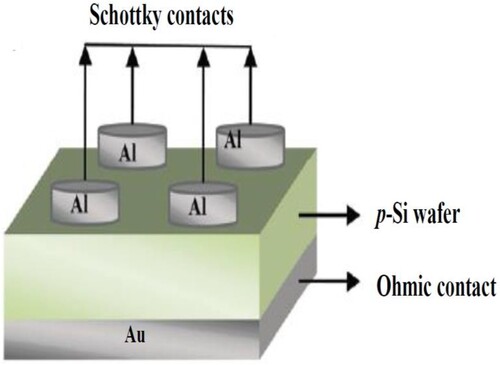
The deposition was done at ∼10−6 mbar at the rate of 1 Å s−1. The process of deposition was conducted utilizing the Edwards AUTO 306 thermal vacuum deposition system. Even after etching Si wafers with HF solution, a 10–30 nm thick oxide layer is present on the Si surface (Citation26). Since all the diodes were fabricated under the same conditions, it is assumed that the effects of the layer on diode qualities are common to all the diodes. The diodes fabricated on unimplanted and Fe-implanted p-Si wafer were labelled undoped and Fe-doped diodes, respectively. The schematic diagram of the fabricated Schottky diode is presented in Figure .
Figure 1. Schematic diagram showing Al/p-Si Schottky diodes with circular Schottky contacts (top surface) and ohmic contact (bottom).
2.3 Device irradiation
Schottky diodes fabricated on undoped and Fe-doped p-Si were irradiated with 4 MeV protons. Prior to irradiation, the beam fluence was estimated from the irradiated time (t), beam current (I), and the beam spot area (B) on the target (Citation27) as.
(1)
(1) where, I is the current, q is the ionic charge, and e is the electronic charge. The diodes were placed on a hexagonal carousal sample holder and then inserted into the microprobe chamber. The diodes were subjected to proton-irradiation using an ion implanter at iThemba LABS in Gauteng Province, South Africa. The irradiation involved bombarding the diodes with 4 MeV protons for approximately 4 hours, resulting in a fluence of 1016 p/cm2. The irradiation took place at room temperature (300 K), although it is possible that the sample temperature increased during the process. Throughout the irradiation, the beam current was carefully monitored and recorded to ensure a constant current and consistent fluence for all samples.
2.4 Device characterisation
In this study, I-V and C-V measurements were performed on the devices in a dark and at room temperature. In-house meters were used for current and capacitance measurements, employing the same hardware with software implementation. A LabVIEW program was coded to read the meters connected to the probe station. The device-to-probe contact was accurately determined by enlarging the device under a microscope. To isolate the measurement system from external electromagnetic fields and maintain a dark environment at room temperature, the devices were placed in a test fixture during measurements.
For I-V measurements, a voltage range of 4–4 V was used. Above approximately 0.7 V, the bias voltage had less impact on the tunnelling electron (TE) current, and beyond ±1 V, the forward current saturated due to series resistance
. The reverse current showed less dependence on the applied voltage for diodes fabricated on unimplanted Si material. C-V measurements, on the other hand, were conducted in reverse bias from 0 to 4 V at 5 kHz to investigate the junction properties of the fabricated devices. The measured capacitance was unstable at frequencies higher than 5 kHz, approaching the limit of the measurement system. A frequency of 5 kHz was chosen to minimize the effects of the m-s interface on the capacitance measurement, as charges at the interface couldn't respond to higher-frequency signals (Citation28).
3.0 Results and discussions
Figure shows ln(I)-V characteristics of undoped and Fe-doped p-Si diodes prior to and after proton-irradiation in a semilogarithmic scale. Prior to proton-irradiation, the current trend of Fe-doped p-Si diode increased, indicating that Fe contributes to the generation of carriers that contribute to the measured current. However, after proton-irradiation, a decrease in the current trend is observed with the rate of decrease being higher in the forward current for both diodes. A decrease in the current is due to the radiation-induced defects that are responsible for the recombination of charge carriers leading to a low charge carrier density through space charge region (SCR). A decrease in current was reported before on neutron (Citation29, Citation30) and proton-irradiated diodes (Citation30, Citation31).
Figure 2. ln(I)-V characteristics of the diodes fabricated on undoped (a) and Fe-doped (b) p-Si prior to irradiation and after irradiation.
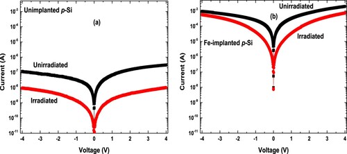
In general, the reverse and forward current of the undoped Si diode decreased by a factor of ∼12 and 31, respectively while in the Fe-doped Si diode, the reverse and forward current decreased by a factor of ∼1.6 and 2.5, respectively at 4 V after proton-irradiation. This insignificant decrease of the current for the Fe-doped Si diode indicates that the radiation effect has been suppressed as a result of Fe in Si. This is due to the fact that Fe-induced defects prevent the further dislodgement of atoms by incident radiation, making the crystal structure stable and independent of incident energetic particles.
In trying to compare the effects of radiation on both diodes, the ratio of unirradiated to irradiated current for both diodes was calculated and plotted as a function of voltage presented in Figure . This type of analysis is used to investigate the range of radiation damage in Si-based device, including m-s interface and SCR. It can be seen from Figure that the ratio is high at low negative voltage, indicating that the damage due to the proton is more on the surface as well as just below the surface in the bulk. Less damage deep in the bulk is because of the low penetration depth of proton. The penetration depth is low since the proton energy is reduced by coulombic interaction with electron clouds of atom constituents on the surface. As a result, the low penetration depth of proton resulted in the damage being low in the Si bulk as observed in high reverse bias. This further shows that the damage due to proton is more on the surface than in the bulk. This is due to the fact that the diode was irradiated from the Schottky contact side of the diode. On forward bias, the trend decreases gently with voltage, indicating that the effect of proton-irradiation reduces due to the recombination of proton-induced charges with interface states on the surface as SCR shrinks.
Figure 3. Current ratio () against voltage (V) for undoped and Fe-doped p-Si diode. Inset: Rescaled ΔI against voltage (V) plot for Fe-doped p-Si diode.
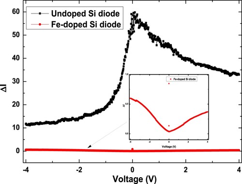
For the Fe-doped p-Si diode, the change in current after proton irradiation remained infinitesimal all through the applied voltages, indicating stability in the m-s interface and SCR regions. The inset of Figure shows that the damage is lower at low voltages, regions associated with the m-s interface. An infinitesimal increase in damage as voltage increases could indicate that Fe implantation has created some paths on the Si surface, hence, proton energy gets through to the bulk since there are limited restrictions. The creation of paths has been reported before (Citation32), where the penetration depth of radiation increases due to doping. As a result, the damage will be deep. However, in this case, the damage in the bulk is infinitesimal, since Fe suppresses or inhibits further damage by radiation.
In the context of proton irradiation at 4 MeV, the radiation lacks the ability to dislodge atoms directly. Instead, it interacts with crystal atoms initially, diminishing its energy and limiting its capacity to displace other atoms. Consequently, structural damage from radiation primarily stems from these crystal atoms rather than the initial proton interaction, occasionally displacing other atoms. In Fe-doped p-Si, the atoms that are dislodged may exhibit reduced movement or slowed kinetics due to prolonged interaction times, particularly influenced by the presence of Fe atoms, further contributing to sporadic displacement events among adjacent atoms.
The I-V characteristics of the diode with series resistance ( (Citation33) is given as
(2)
(2) where the saturation current,
is explained in terms of the Schottky barrier height as
(3)
(3)
In the above relations, V, , k, T,
represents the applied voltage, ideality factor, Boltzmann’s constant, temperature, Richardson constant for p-Si ( = 32 A cm−2 K−2), and diode’s active area ( = 0.00283 cm2), respectively. The ideality factor (
) is obtained from the slope of the forward bias ln (I) – V plot (Citation34, Citation35) using
(4)
(4) The
is calculated by substituting the value of
in Equation (4) as
(5)
(5)
The diode parameters, ,
, and
, for undoped and Fe-doped are presented in Table prior to and after irradiation to investigate the effects of radiation on the electrical properties of the fabricated diodes. In Table , it is observed that
decreased for both diodes after irradiation. Additionally,
and
increased after irradiation. However, the changes in these parameters were relatively insignificant for the Fe-doped p-Si diode. This indicates that the presence of Fe in Si has a suppressive effect on the radiation, as reflected in the observed changes.
Table 1. The diode parameters for undoped and Fe-doped p-Si diodes prior to and after proton-irradiation.
Figure (a) shows the forward bias I-V behaviour of undoped p-Si diode in a logarithmic scale prior to and after irradiation. The forward I-V characteristics of the unirradiated p-Si diode reveal three distinct linear regions, denoted as regions i, ii, and iii, each with different slopes. Region i has a slope, 1.06, close to unity, indicating that the prevailing conduction mechanism is ohmic in this range. In region ii, the slope is 2.58, greater than 2, indicating the dominance of the trapped charge limited current (TCLC) (Citation36, Citation37) conduction mechanism. The slope of region iii is 0.64, suggesting that the current becomes less voltage-dependent, likely due to the presence of at higher voltage (Citation36, Citation37).
Figure 4. Forward bias I-V characteristics of the diodes fabricated on undoped (a) and Fe-doped (b) p-Si diode prior to and after irradiation.
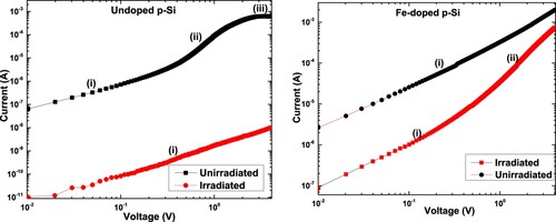
An ohmic region indicates that the thermally generated current dominates the injected free carrier-generated current in the SCR (Citation37). However, the region where TCLC dominates indicates a modification of space charge limited current (SCLC) with exponent trap distribution contributing to the current (Citation38). In this region, the injected free carrier is higher than the thermally generated carrier (Citation32, Citation37). According to the SCLC mechanism, as the applied voltage increases, there is a corresponding increase in the injection of charge carriers from the electrode to the SCR. The forward bias I-V characteristics of the proton-irradiated p-Si diode exhibit a slope of unity throughout the entire voltage region, indicating the conduction mechanism is dominated by the ohmic mechanism. The ohmic behaviour observed all through the voltage range is an indication of a high density of g-r centres induced by irradiation in Si material (Citation8, Citation29).
Figure (b) shows the forward bias I-V characteristics of the diode fabricated on Fe-doped p-Si prior to proton-irradiation in a logarithmic scale. An ohmic trend is observed in Figure (b), indicating that Fe induces g-r centres. These are defects positioned at the centre of the Si energy gap where the generation rate is the same as the recombination rate of charge carriers. These defects have been found to be responsible for radiation-hardness of the material since the conductivity was independent of incident radiation. It must be noted that ohmic I-V characteristics observed on irradiated undoped Si-based diode could indicate that 4 MeV proton-irradiation is also responsible for g-r centres. A similar conjuncture was presented before based on the diodes irradiated with 1 MeV neutrons (Citation8). After proton-irradiation, two regions were observed with slopes of 1.05 and 1.83 respectively on Fe-doped p-Si diode. The slope of the second region is higher, indicating a possibility of atomic dislodgement on the surface where the density of Fe is low, however, the conduction mechanism in the bulk does not change. Unlike in Figure (a), where the diode conduction mechanism changed after proton-irradiation, the change in diode conduction mechanism of Fe-doped p-Si is infinitesimal after proton-irradiation because defects have already been inhibited by Fe, thereby, hindering the formation of any other defects to change the electrical properties of the Si-based device as a result of proton-irradiation. This confirms that the effect of irradiation on the conduction mechanism of Fe-doped p-Si diode has been suppressed.
The C-V characteristics of the diodes fabricated on undoped and Fe-doped p-Si diode prior to and after irradiation are presented in Figure (a, b), respectively. As observed in Figure (a), the capacitance of unirradiated p-Si diode decreases with reverse voltage. Four regions were observed on the C-V trend of unirradiated p-Si diode. The first region (0–0.30 V) shows a steep fall in capacitance, suggesting that the region is associated with the interfacial layer with interface state charges being dominated by metal electrons, hence the electrons are quick to be withdrawn due to the high mobility of electrons. The second region (0.31–0.93 V) shows that the rate of decrease in capacitance has reduced, indicating that the interface state charges are being dominated by ionized acceptors, hence slow to be withdrawn as a result of the low mobility of holes. The third region (0.94–2.50 V) shows a continuous decline in capacitance, indicating that carriers are being withdrawn from the SCR as it tends towards saturation in the fourth region (1.2–4 V) where limited carriers are available for withdrawal.
Figure 5. C-V characteristics of the diodes fabricated on undoped (a) and Fe-doped (b) p-Si prior to and after irradiation. Inset: Rescaled C-V characteristics of proton-irradiated p-Si diode.
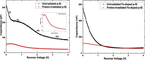
The effect of irradiation is observed by a low-voltage capacitance peak. This peak has been observed before (Citation39) and it is attributed to the interface state charges (Citation40). The low-voltage capacitance peak is due to the damage on the surface resulting in minority carriers with negative charges to increase the capacitance at low voltage. However, the capacitance decreased drastically after proton-irradiation all through the voltage regions, indicating a recombination of charge carriers due to radiation-induced defects that were earlier reported in the I-V results, thereby confirming the consistency of both I-V and C-V techniques.
Figure (b) shows that the capacitance of unirradiated Fe-doped p-Si has increased significantly, suggesting that Fe generates charge carriers in Si. Also, the decrease in capacitance trend is smooth compared to the trend observed on undoped diode where different regions were observed. The smoothness in the capacitance trend in Fe-doped diode could indicate that when conductivity is dominated by a defect in the bulk, the interface states become inactive. However, the capacitance trend starts to saturate after ∼ V, indicating a full depletion of the SCR at this voltage. The saturation observed at the lower voltage upon Fe-doping indicates that the defects that are induced by Fe are responsible for the reduction of FDV. A decrease in FDV indicates that the full depletion of SCR can be achieved with a relatively low applied voltage after Fe doping. A low FDV indicates an improvement in the sensitivity of the fabricated device, though the I-V result showed that the reverse and forward current increased after Fe-doping. After proton-irradiation, a drastic decrease in capacitance is observed at low voltage region, where the density of Fe is low, hence, high atomic dislodgement on the surface. However, the damage is compressed in the bulk (high voltage range), since the presence of Fe prevents the atoms from being dislodged, hence the stability of the crystal structure of the material. Thus, the instability of the material can be explained by the independence of diode capacitance at high voltages. The Fe-doped p-Si diode sustains minimal surface damage after proton-irradiation, as the presence of Fe prevents atom displacement. In comparison with the undoped p-Si diode which exhibits both surface and bulk damage after irradiation, caused by atom knocking due to irradiation, while Fe-doped diode suffers only surface damage.
The C−2−V characteristics of the undoped and Fe-doped p-Si diode prior to and after proton-irradiation obtained from the C−V curves at room temperature are given in Figure . As seen in Figure (a), the C−2−V characteristics showed two linear regions, indicating that the doping density is not uniform. The first linear region could be attributed to the interface state density with electron dominating in the SCR on the Si side. The second linear region is observed at the high voltage region, indicating that the doping profile is uniform over a large area of the SCR (Citation41). Three linear regions were observed on the C−2−V characteristics of the Fe-doped p-Si diode presented in Figure (b). Region (i) has reduced due to defects induced by Fe that has decreased electrons on the surface reducing the impact of negative charge interface states.
Figure 6. C−2-V characteristics of the diodes fabricated on undoped (a) and Fe-doped (b) p-Si prior to irradiation and after irradiation.
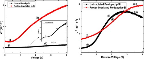
A conductivity-type inversion is observed in the region (iii), indicating that electrons due to Fe doping dominating conduction in the region (Figure (b)). This observation suggests that implanting Si with Fe changes the conductivity-type from p – to n-type by creating defects that induce minority carriers. A similar conductivity-type inversion has been reported before (Citation42), demonstrating that Fe has similar effects in Si just like Pt and Au. Diodes showing conductivity-type inversion have been found resistant to radiation damage (Citation10, Citation43, Citation44), which is attributed to the radiation hardness of the Si-based devices.
Diode parameters from the C-V plots will be obtained from the second linear region of the plots. By applying a linear fit to these linear regions doping concentration () can be evaluated (Citation27, Citation39) as
(6)
(6) The SCR width (
) is also evaluated from the linear regions (Citation33, Citation39) using
(7)
(7) where
is the dielectric constant of the semiconductor and
is the permittivity in a vacuum.
The diode parameters such as and
for undoped and Fe-doped are presented in Table prior to and after irradiation to establish the suppression effect of Fe in Si-based diodes. The parameters given in Table are evaluated from the high voltage region as it is believed that this high voltage region is associated with the SCR. As seen in Table , the change in the evaluated parameters after proton-irradiation is lower on Fe-doped p-Si diode, confirming that radiation has been suppressed in the Fe-doped p-Si diode due to Fe doping. An infinitesimal change of the diode parameters for Fe-doped diode indicates that the SCR is stable and not affected by incident radiation. A very high value of
of Fe-doped Si diode indicates that a significant amount of Fe atoms has been incorporated into the Si lattice due to the high doping fluence. This high concentration of dopant atoms has significantly altered the electrical properties of the Si material. As observed, the carrier concentration has increased, thereby modifying the material's conductivity and possibly affecting its radiation hardness and electronic properties. However, the high doping levels have also introduced challenges such as increased leakage currents and potential degradation of device performance, highlighting the importance of carefully optimizing doping concentrations to achieve desired material characteristics without compromising device functionality.
Table 2. The diode parameters for undoped and Fe-doped p-Si diodes prior to and after proton-irradiation evaluated from -V plot.
4.0 Conclusion
Using I-V and C-V techniques, we studied the effects of 4 MeV proton-irradiation of undoped and Fe-doped Si-based diodes. The decrease in reverse and forward current is less pronounced in Fe-doped p-Si diode compared to undoped p-Si diode after proton-irradiation. Additionally, the evaluated diode parameter of undoped p-Si diode shows a greater rate of change after proton-irradiation compared to Fe-doped p-Si diode. Notably, the diode conduction mechanism remains constant in Fe-doped p-Si diode after proton-irradiation, whereas it changes in undoped diodes. Furthermore, we observed that the SCR's capacitance remains constant after proton-irradiation of Fe-doped Si diode. These results all confirmed the suppression of the irradiation effect on the electrical properties of the diodes, indicating an improved stability of Fe-doped Si diode. The suppression effect is due to the Fe-induced defects already present in Si before irradiation, thereby, hindering the formation of any other defects by proton-irradiation. While Fe is a suitable dopant, akin to Au and Pt, for enhancing the radiation hardness of Si material, its high leakage current implies that radiation hardness comes at the expense of sensitivity. Therefore, further studies are needed to investigate the effects of different doses of Fe doping in Si.
Acknowledgements
The authors are grateful for the valuable assistance provided by Dr. Morgan and Mr. Tony from iThemba LABS in South Africa with device irradiation and Fe implantation. Additionally, the authors appreciate the support of Profs. Auret and Diale from the University of Pretoria for their assistance during diode fabrication.
Disclosure statement
No potential conflict of interest was reported by the authors.
References
- Garcia-Sciveres, M.; Wermes, N. A Review of Advances in Pixel Detectors for Experiments with High Rate and Radiation. Reports Prog. Phys. 2018, 81 (6), 066101.
- Sadrozinski, H.F.W. Applications of Silicon Detectors. IEEE Trans. Nucl. Sci. 2001, 48, 933–940.
- Moser, H.G. Silicon Detector Systems in High Energy Physics. Prog. Part. Nucl. Phys. 2009, 63, 186–237.
- Vittone, E.; Lopez, J.G.; Jaksic, M.; Ramos, M.J.; Lohstroh, A.; Pastuovic, Z.; Rath, S.; Siegele, R.; Skukan, N.; Vizkelethy, G.; etal Determination of Radiation Hardness of Silicon Diodes. Nucl. Instruments Methods Phys. Res. Sect. B Beam Interact. with Mater. Atoms 2019, 449, 6–10.
- McPherson, M.; Sloan, T.; Jones, B.K. Suppression of Irradiation Effects in Gold-Doped Silicon Detectors. J. Phys. D. Appl. Phys. 1997, 30, 3028–3035.
- Parida, M.K.; Sundari, S.T.; Sathiamoorthy, V.; Sivakumar, S. Current–Voltage Characteristics of Silicon PIN Diodes Irradiated in KAMINI Nuclear Reactor. Nucl. Instruments Methods Phys. Res. Sect. A Accel. Spectrometers, Detect. Assoc. Equip. 2018, 905, 129–137.
- Bergholz, W. Defect Engineering in Silicon Materials. In Defects and Impurities in Silicon Materials. Lecture Notes in Physics; Springer: Tokyo, 2015; Vol. 916, pp 431–487.
- Litovchenko, P.G.; Groza, A.A.; Lastovetsky, V.F.; Barabash, L.I.; Starchik, M.I.; Dubovoy, V.K.; Bisello, D.; Giubilato, P.; Candelori, A.; Rando, R.; Litovchenko, A.P.; Khomenkov, V.; Wahl, W.; Boscardin, M.; Zorzi, N.; Dalla Betta, G.-F.; Cindro, V.; Mikelsen, M.; Monakhov, E.V.; Svensson, B.G. Radiation Hardness of Silicon Detectors Based on Pre-irradiated Silicon. Nucl. Instruments Methods Phys. Res. Sect. A Accel. Spectrometers, Detect. Assoc. Equip. 2006, 568, 78–82.
- Moloi, S.J.; McPherson, M. Reverse Annealing Studies of Irradiated Silicon by use of Current–Voltage Measurements. Nucl. Instruments Methods Phys. Res. Sect. B Beam Interact. with Mater. Atoms 2019, 440, 64–67.
- Msimanga, M.; McPherson, M. Diffusion Characteristics of Gold in Silicon and Electrical Properties of Silicon Diodes Used for Developing Radiation-Hard Detectors. Mater. Sci. Eng. B 2006, 127, 47–54.
- Moloi, S.J.; McPherson, M. Current–Voltage Behaviour of Schottky Diodes Fabricated on p-Type Silicon for Radiation Hard Detectors. Phys. B Condens. Matter 2009, 404, 2251–2258.
- Dixon, R.L.; Ekstrand, K.E. Gold and Platinum Doped Radiation Resistant Silicon Diode Detectors. Radiat. Prot. Dosimetry 1986, 17, 527–530.
- Kolbesen, B.O.; Bergholz, W.; Wendt, H. Impact of Defects on the Technology of Highly Integrated Circuits. Mater. Sci. Forum 1989, 38, 1–12.
- Istratov, A.A.; Hieslmair, H.; Weber, E.R. Iron and Its Complexes in Silicon. Appl. Phys. A 1999, 69, 13–44.
- Graff, K.; Pieper, H. The Properties of Iron in Silicon. J. Electrochem. Soc. 1981, 128, 669–674.
- Graff, K. Metal Impurities in Silicon-Device Fabrication, Vol. 24, Springer Science & Business Media: Heidelberg, 2013.
- Beeler, F.; Andersen, O.K.; Scheffler, M. Theoretical Evidence for Low-Spin Ground States of Early Interstitial and Late Substitutional 3 d Transition-Metal Ions in Silicon. Phys. Rev. Lett. 1985, 55, 1498–1501.
- Weber, E.R. Transition Metals in Silicon. Appl. Phys. A 1983, 30, 1–22.
- Gilles, D.; Bergholz, W.; Schröter, W. Diffusion of Manganese in Silicon Studied by Deep-Level Transient Spectroscopy and Tracer Measurements. J. of Appl. Phys. 1986, 59, 3590–3593.
- Nakashima, H.; Sadoh, T.; Tsurushima, T. Hole Traps of Metastable Iron-Boron Pairs in Silicon. J. of Appl. Phys. 1993, 73, 2803–2808.
- Brotherton, S.D.; Bradley, P.; Gill, A.; Weber, E.R. Electrical Observation of the Au-Fe Complex in Silicon. J. of Appl. Phys. 1984, 55, 952–956.
- Jones, B.K.; McPherson, M. Radiation Damaged Silicon as a Semi-Insulating Relaxation Semiconductor: Static Electrical Properties. Semicond. Sci. Technol. 1999, 14, 667–678.
- Bera, B. Silicon Wafer Cleaning: A Fundamental and Critical Step in Semiconductor Fabrication Process. Int. J. Appl. Nanotechnol. 2019, 5, 8–13.
- Tanrıkulu, E.E.; Demirezen, S.; Altındal, Ş; Uslu, İ. Analysis of Electrical Characteristics and Conduction Mechanisms in the Al/(% 7 Zn-Doped PVA)/p-Si (MPS) Structure at Room Temperature. J. of Mat. Scien.: Mat. in Electron. 2017, 28, 8844–8856.
- Sze, S.M.; Ng, K.K. Physics of Semiconductor Devices; John wiley & sons: New York, 1981.
- Siad, M.; Keffous, A.; Mamma, S.; Belkacem, Y.; Menari, H. Correlation Between Series Resistance and Parameters of Al/n-Si and Al/p-Si Schottky Barrier Diodes. Appl. Surf. Sci. 2004, 236, 366–376.
- Knoll, G.F. Radiation Detection and Measurement; John Wiley & Sons: New York, 2010.
- Yüksel, ÖF; Selçuk, A.B.; Ocak, S.B. Investigation of Diode Parameters Using I-V and C-V Characteristics of In/SiO2/p-Si (MIS) Schottky Diodes. Phys. B Condens. Matter 2008, 403, 2690–2697.
- Bisello, D.; Candelori, A.; Kaminski, A.; Pantano, D.; Rando, R.; Wyss, J.; Andrighetto, A.; Cindro, V. Radiation Effects on Standard and Oxygenated Silicon Diodes. In 2001 IEEE Nuclear Science Symposium Conference Record (Cat. No. 01CH37310); IEEE: San Diego, 2001; vol. 1, pp. 189–196.
- Gurimskaya, Y.; de Almeida, P.D.; Garcia, M.F.; Suau, I.M.; Moll, M.; Fretwurst, E.; Makarenko, L.; Pintilie, I. Radiation Damage in p-Type EPI Silicon Pad Diodes Irradiated with Protons and Neutrons. Nucl. Instruments Methods Phys. Res. Sect. A Accel. Spectrometers, Detect. Assoc. Equip. 2020, 958, 162221.
- Oeba, D.A.; Bodunrin, J.O.; Moloi, S.J. Electrical Properties of 3 MeV Proton Irradiated Silicon Schottky Diodes. Phys. B Condens. Matter 2021, 610, 412786.
- Davies, G.; Hayama, S.; Murin, L.; Krause-Rehberg, R.; Bondarenko, V.; Sengupta, A.; Davia, C.; Karpenko, A. Radiation Damage in Silicon Exposed to High-Energy Protons. Phys. Rev. B 2006, 73, 165202.
- Sze, S.M. Semiconductor Devices: Physics and Technology; John Wiley & Sons: New York, 2008.
- Elnobi, S.; Dongol, M.; Soga, T.; Abuelwafa, A.A. ChargeTransport, Photoresponse and Impedance Spectroscopy for Au/NiTPP/n-Si/Al Diode. J. Alloys Compd. 2023, 965, 171235.
- Güllü, Ö; Okumuş, M.; Ava, C.A. Investigation of the Structural and Morphological Features of TiO2: 8OBA Composites for MIS Semiconductor Diodes. Mater. Sci. Eng. B 2023, 289, 116286.
- Rosales-Quintero, P.; Torres-Jacome, A.; la Hidalga-Wade, D.; Zúñiga-Islas, C.; Calleja-Arriaga, W.; Reyes-Betanzo, C. Current Conduction Mechanisms in n-Type α-SiGe: H/p-Type c-Si Heterojunctions. Superf. y Vacío 2008, 21, 1.
- Rose, A. Space-Charge-limited Currents in Solids. Phys. Rev. 1955, 97, 1538–1544.
- Bodunrin, J.O.; Moloi, S.J. Current-Voltage Characteristics of 4 MeV Proton-Irradiated Silicon Diodes at Room Temperature. Silicon 2022, 14, 10237–10244.
- Cetin, H.; Şahin, B.; Ayyildiz, E.; Türüt, A. Ti/p-Si Schottky Barrier Diodes with Interfacial Layer Prepared by Thermal Oxidation. Phys. B Condens. Matter 2005, 364, 133–141.
- Taşçıoğlu, İ; Soylu, M.; Altındal, Ş; Al-Ghamdi, A.A.; Yakuphanoglu, F. Effects of Interface States and Series Resistance on Electrical Properties of Al/Nanostructure CdO/p-GaAs Diode. J. Alloys Compd. 2012, 541, 462–467.
- Mahato, S.; Biswas, D.; Gerling, L.G.; Voz, C.; Puigdollers, J. Analysis of Temperature Dependent Current-Voltage and Capacitance-Voltage Characteristics of an Au/V2O5/ n -Si Schottky Diode. AIP Adv. 2017, 7, 1.
- Carchano, H.; Jund, C. Electrical Properties of Silicon Doped with Platinum. Solid State Electron Devices 1970, 13, 83–90.
- Bodunrin, J.O.; Oeba, D.A.; Moloi, S.J. Current-Voltage and Capacitance-Voltage Characteristics of Cadmium-Doped p-Silicon Schottky Diodes. Sens. Actuators, A 2021, 331, 112957.
- Pitzl, D.; Cartiglia, N.; Hubbard, B.; Hutchinson, D.; Leslie, J.; O'Shaughnessy, K.; Rowe, W.; Sadrozinski, H.F.-W.; Seiden, A.; Spencer, E.; Ziock, H.J.; Ferguson, P.; Holzscheiter, K.; Sommer, W.F. Type Inversion in Silicon Detectors. Nucl. Instruments Methods Phys. Res. Sect. A Accel. Spectrometers, Detect. Assoc. Equip. 1992, 311, 98–104.