
ABSTRACT
The detection of surface cracks at or close to sample edges is a challenging problem because the interaction of the eddy current with the sample edge can make it difficult to distinguish changes in the eddy current signal due to a defect. Samples with poor electrical conductivity such as titanium alloys used extensively in aerospace applications can be more difficult to inspect due to the low amplitude eddy currents induced in them and increased electromagnetic skin depths due to lower electrical conductivity. As fatigue surface cracks or manufacturing surface defects can often occur close to edges, the challenges of detecting small defects close to sample edges is an important research area to address. High-frequency eddy currents of over 10 MHz are used in a transmit-receive configuration using two solenoid type coils adjacent to each other. While conventional eddy current sensors are commonly designed for operating at frequencies into the low MHz region, the supporting electronics here will be positioned immediately behind the coils to improve electrical stability and reduce induced noise. The magnitude and phase of the voltage on transmit and receiver coils are measured, and finite element modelling is used to validate the experimental measurements and gain insight into the system behaviour. Small defects of down to 1 mm are easily detected, on the edge and at the corner of a titanium alloy sample with excellent signal-to-noise.
Introduction
Many safety-critical components in the aerospace or power generation industries are made from titanium alloys, which have lightweight, high strength and excellent corrosion resistance [Citation1,Citation2]. But they suffer from fatigue of manufacturing defects that can lead to the generation of surface-breaking cracks [Citation3]. Techniques used for surface crack detection include penetrant testing (PT), magnetic particle inspection (MPI) and magnetic flux leakage (MFL) [Citation4]. Unfortunately, the PT method needs critical surface cleaning and is only sensitive to defects open to the surface, while MPI and MFL methods are restricted to ferromagnetic materials. Whilst there are reports of using ultrasound to detect small surface-breaking defects [Citation5], it is rarely in practice used in industry but is obviously a dominant method used in inspecting samples for volumetric defects.
Table 1. Minimum and maximum values for the experimental edge defect data.
Table 2. Minimum and maximum values for the experimental edge data without defect.
There are derivates of the main inspection methods mentioned such as visual inspection being improved by machine vision [Citation6], showing promise with developments in AI. There are many advantages to using this approach, such as its high sensitivity and fast detection speed. However, it is also subject to the same disadvantages of visual inspection; it is susceptible to illumination and image noise, and obviously, it only responds to the very top of the sample surface.
Eddy current testing (ECT) has been used extensively for surface defect detection and is a well-established technology [Citation7], that is ideally suited to the detection of surface cracks.
However, in ECT, as a coil carrying alternating electrical current approaches the sample edge, the electromagnetic fields from the coil and eddy current in the sample interact with the edge in a different way to when the coil is distant from the edge. This change in the boundary conditions gives rise to a change in the eddy current and the electrical properties of the coils themselves and can be observed some distance away from the sample edge, as the eddy current can extend significantly beyond the footprint of the coil on the sample. This extension distance is affected by coil geometry and lift-off but is mainly dependent on the electromagnetic skin depth of the sample in practical use. The response to the edge has the potential to mask the response to the defect at or close to the edge [Citation8].
As such, most research focuses on inspecting defects far from any edge [Citation9]. There are, nevertheless, some examples where it is used to detect defects near an edge. T Dogaru et al. (2000) [Citation10] detected millimeter length edge defects on an aluminium plate, using a magnetoresistance (MR) based eddy current sensor. While Wang et al. (2017) [Citation11] looked at subsurface defects at the edge of a titanium alloy block, using an absolute probe. Additionally, Xie et al. (2020) [Citation9] looked at improving sensor parameters to enhance the capability for detecting defects close to an edge on a titanium alloy, although this work uses the finite element modelling method, where their optimisation work was based on the morphology of the signal, rather than experimental SNR. Moreover, papers exist that study defects in difficult locations, such as in, or around bolt holes [Citation12], and on turbine blades [Citation13].
Additionally, differential coils may be used to improve sensitivity to defects near an edge. Eua-Anant et al. (1999) [Citation14] describes how cracks often develop near slot edges in jet engines discs. They identify differential probes to be useful in improving sensitivity to the crack in such a situation. In particular, split-D differential eddy current probes may be used, which can help minimise the edge effects. Though, it is usually necessary to ensure good alignment with the edge when using such coils.
Other solutions include using more complex coils shapes. For example, rectangular planar coils were used by Fava and Ruch (2004) [Citation15] to minimise the edge effect. In addition, the use of high magnetic permeability cores and flux focusing can be used to reduce the edge effect by focusing the eddy current into a smaller region [Citation16].
This paper shows experimental results supported by simulations, where we report improved defect detection and SNR for a defect located at a straight edge, or a corner on a titanium plate, by operating at MHz frequencies. This approach is agnostic in that it can be applied to other coil types and scan techniques to improve sensitivity, by concentrating the eddy current more directly under the footprint of the coil being used.
Increasing the frequency of the eddy current coil obviously increases the frequency of the magnetic field produced by the coil and consequently of the electrical field produced in the sample that drives the eddy current in the sample, which confines the eddy current to a shallower skin depth, providing increased sensitivity to shallow defects, and also has the effect that it confines the lateral extent of the eddy current so that more of the eddy current is flowing directly under the driving coils [Citation17]. This will particularly help with testing titanium alloys, which as a lower conductivity material can be more difficult to inspect using ECT. The same point applies to the MR technique discussed earlier, where lower conductivity materials such as titanium alloys have been found to be more difficult to inspect than, for example, aluminium [Citation18].
Operating at high frequencies to detect surface flaws has been reported previously for carbon fibre materials, where Heuer et al. (2011) [Citation19] used the EddyCus system to detect flaws in the range of a few millimetres by operating at 2–10 MHz, and Hughes et al. (2016) [Citation17] used frequencies over 15 MHz, where they also used high-frequency eddy current measurements on titanium alloys to improve sensitivity to small surface-breaking defects.
However, in real systems, capacitive effects and inductive coupling throughout the entire system, will also typically lead to an increase in the level of electrical noise with increased frequency and thus, a lower SNR in eddy current measurements. These capacitive, inductive and also resistive elements are present in the cables connecting the eddy current coils to the electronics, and the coils themselves.
We, therefore, have two competing effects to consider when examining how the SNR will change as eddy current frequency increases, for detecting defects close to the sample edge. On the one hand, the increase in frequency concentrates the eddy current more under the footprint of the coil, improving the SNR for a defect close to the edge, but on the other hand, the SNR will also tend to decrease as frequency increases.
The size of the coil or the width of the coil (or eddy current) should also be considered. The skin depth for a plane wave in titanium is approximately 0.33 mm at 1 MHz and 0.1 mm at 10 MHz, which is smaller than the typical diameter of an eddy current coil, which in our case is 0.55 mm. At some point, the diameter of the eddy current coil will become the limiting factor (as will be seen in the results), and so one should expect that when considering all these phenomena together, there will be an optimum frequency for a given coil design and target defect. This is what we observe experimentally in measurements of defects close to a sample edge.
For the supporting simulation work, numerous publications consider analytical and numerical or finite-element-type models to describe eddy current coil behaviour [Citation20–22] including Theodoulidis et al. (2009) who uses a quasi-analytical approach to find the electromagnetic field near the edge of a sample [Citation23], which is verified by comparing coil impedance measurements from finite element modelling, and Bowler (2012) [Citation24] who provides calculations for the electromagnetic field due to an edge crack. In this paper, COMSOL is used to model the eddy current coils and their interaction with the sample. One of the challenges of most finite element models is that in general, modelling accuracy decreases as frequency increases or component size decreases, and it can be difficult to incorporate noise effects in the whole system. Nevertheless, finite element modelling supports the experimental results obtained. Even when considering the eddy current coil as an idealised inductor of finite width with no electrical noise sources in the model, beyond a certain frequency, there are diminishing returns to the spatial localisation of the defect signal.
When using an eddy current system that presents the data as a Lissajous figure, the system is displaying the magnitude and phase simultaneously, and a skilled operator can interpret such signals with a high degree of success. For a comparative and quantitative study, we need to capture and store the magnitude and phase data from an eddy current measurement. In the measurements reported here, we use two separate coils, placed adjacent to each other, for the generation and detection of eddy currents, as has been reported previously [Citation17]. In this paper, we measure and record the magnitude and phase information relative to the drive current reference signal for both the generator and detector coils. The approach in these trials is to keep and analyse all of the data possible, to investigate which measurements might, for example, have better SNR, or be more robust to stand-off variation.
Method
Eddy current coils
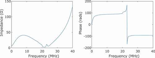
In these experiments, two solenoid-type coils are used, wrapped around an air-cored former. The 1 mm long coils consist of five layers, of 20 turns per layer to give a total number of 100 turns. The inner and outer diameters of the coils are 0.315 mm and 0.55 mm, respectively. One coil is used as the generator and positioned immediately adjacent to it is a detector coil, as shown schematically in . The impedance response with frequency is measured across a coil in the probe and is shown in . It can be seen in this figure that the first resonance occurs at a frequency above that used for the scans.
Figure 1. Probe consists of transmitter (Tx) and receiver (Rx) coils placed in close proximity. Each coil is made using 0.025 mm diameter wire wound into 100 turns. The dimensions of the coils are an inner diameter of 0.315 mm, an outer diameter of 0.55 mm and a height of 1 mm.
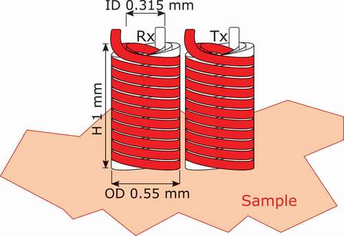
Figure 2. Measured impedance with frequency.
While it may be entirely appropriate to consider alternative probe coil types and shapes such as differential type coils, the eddy current coil arrangement used here is kept simple, as the purpose of the paper is to investigate improvements of detection for edge/corner defects due to the use of higher eddy current frequencies. This approach of concentrating the eddy current more tightly under the generating coil by using higher frequencies is agnostic, and using different coil designs at higher frequencies is a sensible consideration for further work. The simplicity of the coil design reported here also helps to reduce the complexity of the computational simulations that will be performed to support the hypothesis of improved eddy current confinement by increasing drive frequency.
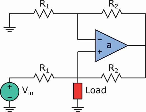
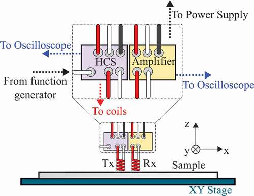
The electrical setup is the same as has been described in earlier publications [Citation17] and is shown in . The coil is driven by a voltage-controlled Howland constant amplitude current source (HCS), and the detection coil is connected to an amplifier, which is connected to an oscilloscope. The data is stored on a computer using MATLAB, which also controls the scanning of the eddy current coils over a sample on an XY table. The voltage magnitude (mag.) and phase relative to the driving voltage are recorded for both coils.
Figure 3. Schematic circuit diagram of Howland Current Source (HCS).
Simulated defects
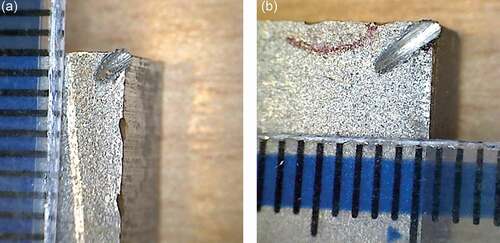
For this preliminary proof-of-concept experiment, a finer slot was cut at the edge of a longer section of a 5 mm thick titanium sample (99.6+% purity) using laser micro-machining and two crude defects were machined on the corners of the same sample. A photograph of the edge defect is shown in and a photograph of the corner defect is shown in .
Figure 4. Photographs of edge defect from two views. (b) is orientated to aid with comparison with the 2D plots.
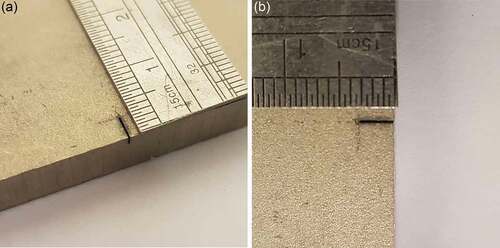
Figure 5. Photographs of the two crudely made corner notches with notch 2 (b) being slightly longer than notch 1 (a). The intervals on the ruler placed in the images are 1 mm apart.
The laser micro-machined slot was 3 mm long, orientated perpendicular to the sample edge, to a depth of 1 mm, with a gap at the opening of 0.5 mm, which decreases with depth due to the conical profile of the focused laser beam used to produce the cut.
The two crudely made slots were prepared using a small circular abrasive disc of thickness 0.6 mm, to create a simulated defect feature that is more like a void than a crack in nature. The width of each notch is approximately 0.8 mm ± 0.1 mm and the depth is approximately 1 mm. The lengths of the notches were 1 mm and 2 mm, and both were positioned on the corner of the sample. So there are edge effects from two edges at the same time, making the measurement more challenging. The notches are called notch 1 and 2 respectively.
Experimental setup
In the experiments, the notches were scanned using the eddy current probe described in , with a scanning area of 10 mm x 10 mm, at a scanning step of 0.1 mm, to create scans consisting of 100 × 100 points. The coils were scanned across the sample and over the edge of the sample into free space. The data were collected using a digital oscilloscope connected to a computer that recorded the results. The HCS was driven using the output voltage of an arbitrary function generator, driven as a continuous sine wave at a peak-to-peak voltage of 2 V for the scans with a defect present. This was later reduced to 1 V peak-to-peak for the defect-free sample scans, as the signal from the HCS started to generate a distorted sinusoidal current at higher voltages. The drive frequency of the voltage was changed so that we were able to obtain scans of the simulated defect at frequencies of 1 MHz, 5 MHz, 10 MHz, 15 MHz and 20 MHz. A diagram of the setup is shown in , which is similar to recently published work [Citation25]. The orientation of the probe relative to the defect is also the same, where the T/R probe is aligned with the notch so that the responses are aligned along the y-direction.
Figure 6. Experimental setup. Phase measurements are taken with respect to the signal from the function generator.
Finite element modelling
The response of the eddy current sensors to the edge defect slot was simulated using the multiphysics finite element program COMSOL, and the model setup is shown in , where the two coils Rx and Tx can just be seen in the centre of the image. The geometry was defined as two air-cored coils placed next to each other and centred above a rectangular sample with a small rectangular intrusion on its surface representing a defect. The coils use COMSOL’s multi-turn coil feature, where the current density is assumed to be homogeneous instead of explicitly modelling each turn. The current of one of the coils is set to have a constant amplitude of 2 mA for the scans with a defect and reduced to 1 mA for the flaw-free scans since the reference voltage to the HCS was halved. To simulate the scan process, the two coils are moved along the x- and y-directions simultaneously, with 0.1 mm steps. The voltages across each coil are measured at different locations, for frequencies of 1 MHz, 5 MHz, 10 MHz, 15 MHz and 20 MHz. The phase of the voltage signal is taken with respect to the system reference signal, whereby the phase of the current is 0 rads, but experimentally, the phase is taken with respect to the function generator that is used to provide a sharper signal to trigger from.
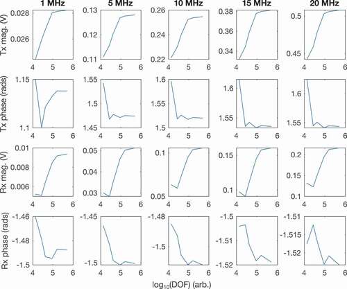
The model was automatically meshed using COMSOL’s physics controlled mesh, solved in the frequency domain and the solver chosen by COMSOL was BiCGSTAB. At the selected coordinates, the mesh size was varied to ensure there were acceptable mesh settings and it was checked that this did not change the results significantly (this is shown for a location on the defect in ). By default, COMSOL ensures that the result needs to meet a certain convergence threshold i.e. where the estimated error between the current solution and exact solution is below a defined tolerance (relative tolerance was kept at the default of 0.001). Results below this threshold are disregarded.
Figure 7. Diagrams showing the location of the sample, defect and coils in the COMSOL FE model for (a) a defect on a single edge and (b) a corner defect. The diagrams are shown for the (0,0) mm location.
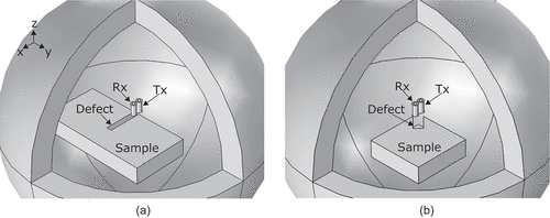
Figure 8. Plots showing the convergence of the measured variables with increasing mesh density at the centre of the defect, which is located at (−1.5, 0) mm. The measured variable is plotted against the degrees of freedom.
Results
Experimental results from the defect on the plate edge
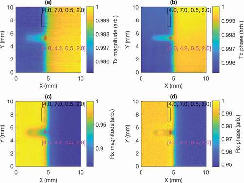
shows the scanning results of the edge defect shown in shows the scan without a defect for comparison. The signals were normalised for quantitative comparison at different frequencies, but show the minimum and maximum values for the raw data from each respective scan before normalisation. To try to compare these plots, we define an approach used to quantify the maximum signal amplitude of the reading on the defect to the noise level in a comparable region on a plate edge, but away from the defect. In practice quantifying SNR is quite complex, and in this scenario and the problem is that there is no defined way of trying to find the SNR in these types of scans. To try to keep this definition simple and make it easier for others to compare in independent measurements, the signal amplitude is taken to be the average value of the five largest absolute values of the signal observed in a region on the defect after subtracting the average of a defect-free region. While, the noise is the standard deviation of the amplitude of the signals away from the defective region, see . The regions being considered are given in millimetres as [x position, y position, width, height].
Figure 9. Normalised experimental results for 2D scans on titanium near an edge at varying frequencies. The bottom and left labels are for the x-axis and y-axis respectively. The plots are organised into columns of the same frequency, given by the labels on the top edge. The plots are organised into rows according to the variable being measured as labelled on the right edge. Mag. is short for magnitude.
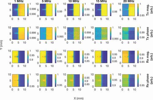
Figure 10. Normalised experimental results for 2D scans on titanium near an edge at varying frequencies. The bottom and left labels are for the x-axis and y-axis, respectively. The plots are organised into columns of the same frequency, given by the labels on the top edge. The plots are organised into rows according to the variable being measured as labelled on the right edge. Mag. is short for magnitude.
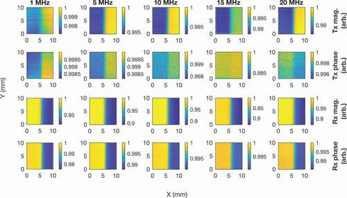
Figure 11. Illustration of the SNR calculation of the scanning results. Shown are the results for 1 MHz, but the regions considered are consistent across all the frequencies considered. The background is defined to be the region in the black box. The noise is taken to be the standard deviation of this region and the average is calculated. This average is used to determine the signal, whereby the signal is taken to be the average of the five largest differences between a value in the magenta box and this average. Here, the plots are normalised and the position of the five signal points are shown as red crosses. As an example, for Tx mag, the five largest differences are 22 x 10−4, 22 x 10−4, 21 x 10−4, 21 × 10−4 and 21 × 10−4. This gives a signal of 21 × 10−4. While, the noise is 14 x 10−4, yielding an SNR of 13.7 dB.
This method might seem a little arbitrary and one would see shifts in the SNR calculation based on the regions chosen, but this approach is consistent and easy for others to reproduce. This will provide some meaningful and reproducible, easy method to quantify the SNR, but when inspecting the image for evidence of a defect, the reader is obviously drawing on a wider set of data and defects are easier to ‘see’ than this simple quantification of SNR might imply. shows the indicative values of SNR in different cases.
Table 3. Indicative SNR values of the edge defect from the experimental results.
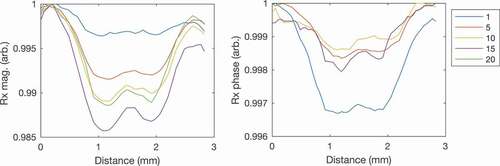
One can see that in the Tx mag. the signal increases with frequency from 1 MHz to 15 MHz before dropping for the highest frequency considered of 20 MHz. Tx phase on the other hand seems to have a decreasing SNR with frequency, which can also be seen in the plots of . This noise seems to be linked to the Tx phase measurement being more sensitive to noise. Along with this, there is an increased localisation of the signal with frequency initially, as one can see the peak of the signal becoming more defined in line scans (see ), before plateauing. The full width at half maximum (FWHM) with increasing frequency through a cross-section at X = 4.5 mm is 1.6 mm, 0.8 mm, 0.7 mm, 0.7 mm and 0.7 mm in the Tx mag., and from 1 MHz to 10 MHz, the FWHM is 0.9 mm, 0.7 mm and 0.7 mm in the Tx phase. The FWHM for the Tx phase is not calculated for 15 MHz and 20 MHz, because the noise at 15 MHz meant the maxima through this cross-section did not coincide in any way with the defect location, and the signal was no longer a peak at 20 MHz. The FWHM is calculated applying a cubic spline interpolation to the cross-section with an interval of 0.0001 mm using ‘spline’ in MATLAB, and then taking the width to be the distance between the locations where the value of the dependent variable is first equal or below the average of the dependant variable’s minimum and maximum when going outwards from the maxima. From this, it is possible to see that it may only be possible to benefit from improved resolution with frequency up to a certain point.
At very high frequencies, one expects the eddy current to be more strongly focused directly under the footprint of the wires of the eddy current coil, and as we decrease the frequency, one would expect the eddy current to gradually spread out laterally from the footprint of the coil. Coil diameter and defect depth and size will also influence the value of frequency at which improvements in signal amplitude change more quickly. Thus, for a smaller coil diameter and thickness of the turns of the coil, and a smaller size defect, one might expect the point at which improvements to the resolution of the coil become diminishing above 10 MHz.
Rx mag. seems to have a similar SNR between 5 MHz and 15 MHz, dropping off either side, while the Rx phase seems best between 5 and 10 MHz. However, there is interesting behaviour where the defect signal rises above both the sample and off sample regions in some of the Rx data. In many of the results, if the defect signal overall rises/falls a corresponding signal change is seen with the eddy current sensors off the part but close to its edge, which made it difficult to distinguish the defect signal from the edge. This interesting behaviour means that we can just pick out the defect as the highest points, see . If a similar approach to the one described before is taken, the SNRs for plots where the defect rises above the background are as given in . Here, the signal is taken as the average difference between the five highest points and the average of the background region, and the noise is taken to be the standard deviation of the background region. Since there are two background regions, on and off the defect, there are two separate SNRs defined per plot. One is based on a background region on the sample and one is based on a background region off the sample. These areas are shown as red and green boxes respectively in . While the task of distinguishing the defect is a combination of comparison of defect signal with both the sample and the off sample regions, the SNRs in based on the sample region could be viewed as more important than that based on the off sample region as the defect signal is clearly above the off sample region, which makes the task of detecting defects more about distinguishing the defect from the sample.
Figure 12. Illustration of the SNR calculation of the scanning results based on the highest points. The background off the sample is defined to be the region in the green box and the background region on the sample is defined to be the region in the red box. Shown are the results for 15 MHz on the receive coil as magnitude (a) and phase (b), but the regions considered are consistent across all the frequencies considered. Here, the plots are normalised and the five highest points are shown as black crosses.
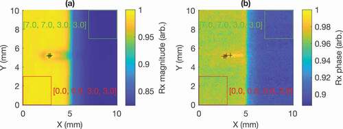
Figure 13. Normalised line scans at constant X extracted from experimental 2D scans shown in , at different frequencies for the edge defect. For this plot, X = 4.5 mm.
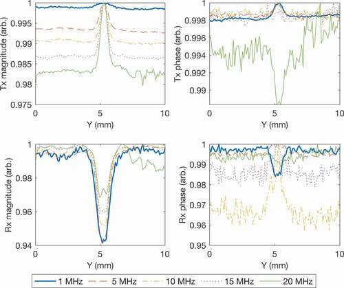
Table 4. SNR for edge defect from the experimental results based on the five largest points. Entries, where the five largest points are not on the defect, are not shown.
A few of the table entries are empty. For 10 MHz, it is possible to see that this is because of the effect of the tilt on the sample. Any small tilt of the sample relative to the probe seems to become more important at higher frequencies. For Rx mag. at 10 MHz, it is possible for the five largest points to coincide with the defect signal if the region considered for analysis is restricted, but removing the top 1 mm strip from the data ensures that the largest two points are on the defect and removing the top 2 mm strip of the data ensures that the largest three points are on the defect. This suggests that the effect of sample tilt, whereby the signal at the top is generally larger than the bottom, is preventing the maximum points from being found on the defect. For the Rx phase measurement at 20 MHz, the plot was too noisy to yield useful data.
From looking at the Rx phase 2D scans along with the SNR calculations, 5 MHz may be an interesting region to look at as the defect signal increases to be above the sample region producing a good SNR. While there may be benefits to going to even higher frequencies, the noise appears to become proportionally higher, and thus choosing the best frequency is a compromise.
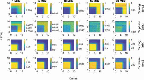
Modelling results from the defect on the plate edge
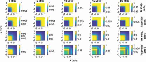
Finite element modelling of the edge notch is shown in and modelling of the edge without a defect is shown in for comparison. The figures are normalised, but the absolute minimum and maximum values are shown in , with the defect present and in without the defect present. The C-scans again show mag. and phase for the generation and detection coils at frequencies of 1 MHz – 20 MHz. The coils dimensions are as specified in the previous section, but these models are not able to simulate the effect of electrical noise and neither the cables nor the electronics are included in this simulation, which is to all intent and purpose noise-free, with the exception of ‘numerical noise’ on the calculated response.
Figure 14. Normalised simulation results for 2D scans on titanium near an edge at varying frequencies. The bottom and left labels are for the x-axis and y-axis respectively. The plots are organised into columns of the same frequency, given by the labels on the top edge. The plots are organised into rows according to the variable being measured as labelled on the right edge. The label mag. is short for magnitude. The coils are on the sample on the left half of each image and off the sample on the right half of each image, and the centre of the pair of coils and the sample edge coincide at (0,0) mm.
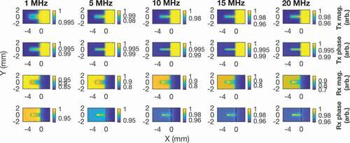
Figure 15. Normalised simulation results for 2D scans on titanium near an edge without the defect present at varying frequencies. The bottom and left labels are for the x-axis and y-axis respectively. The plots are organised into columns of the same frequency, given by the labels on the top edge. The plots are organised into rows according to the variable being measured as labelled on the right edge. The label mag. is short for magnitude. The coils are on the sample on the left half of each image and off the sample on the right half of each image, and the centre of the pair of coils and the sample edge coincide at (0,0) mm.
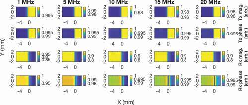
Table 5. Minimum and maximum values for the FEM edge defect data. The Rx mag. data is multiplied by ten to reflect the amplification used on the Rx coil.
Table 6. Minimum and maximum values for the FEM edge data without defect. The Rx mag. data are multiplied by ten to reflect the amplification used on the Rx coil.
These modelling results are consistent with the experimental results reported earlier. The absolute Tx mag. and Rx mag. values in agree with the experimental ones presented in , with magnitude and the general trend of these values increasing with frequency, which is also seen in the experimental results. The exact values would not be expected to be the same, as the model system is idealised. Also, for both the experimental and simulation results, the range for the normalised results for Tx mag. and Rx mag, shown in , increases with frequency. It makes less sense to compare the experimental and modelled absolute values of the phase data, as the phase is compared to the function generator in the experiment, rather than the current, as is the case for the simulation.
Table 7. Range of normalised edge results for the magnitude of transmitter and receiver from experiment.
Table 8. Minimum and maximum values for the raw notch 1 data from experiment.
Table 9. Minimum and maximum values for the raw notch 2 data from experiment.
Table 10. Minimum and maximum values for the raw data without a notch from experiment.
Table 11. Indicative SNR values of corner notch 1 from the experimental results.
Table 12. Indicative SNR values of corner notch 2 from the experimental results.
Table 13. Minimum and maximum values for the FEM notch 1 data. The Rx mag. data is multiplied by ten to reflect the amplification used on the Rx coil.
Table 14. Minimum and maximum values for the FEM notch 2 data. The Rx mag. data is multiplied by ten to reflect the amplification used on the Rx coil.
Table 15. Minimum and maximum values of FEM data for corner scan without notch. The Rx mag. data is multiplied by 10 to reflect the amplification used on the Rx coil.
As before, Tx results become increasingly localised with frequency. The FWHM with increasing frequency is 1.53 mm, 0.92 mm, 0.84 mm, 0.80 and 0.78 mm in the Tx mag., and 0.96 mm, 0.72 mm, 0.66 mm, 0.63 mm, 0.63 mm and 0.62 mm in the Tx phase through a cross-section at X = −1.5 mm (i.e. the cross-section where the centre of the defect and centre of the coils coincide in the x-direction). The FWHM is calculated using the same approach used for the experimental results. Here, the modelling data shows small diminishing improvements in the resolution with frequency.
Additionally, the simulation results for the Rx measurements also display the behaviour whereby the defect transitions to become the maximum signal when going from the lowest frequency. The maximum 5 points are found on the defect signal for all frequencies except 1 MHz, where the maximum points are not on the defect for Rx mag. and only three of the highest point are on the defect for the Rx phase. One can also see a trend, where on the sample and off sample regions become more similar in level for the Rx phase compared to the defect signal with frequency, which helps the defect to stand out. One can see evidence for this in the experimental results, but then the noise is also seen to increase with frequency. The simulation does not take into account the electrical noise induced from capacitive or inductive components of the entire system. As such, a compromise is required between getting the desired behaviour and avoiding noise associated with going to higher frequencies.
Experimental results from the crude defects on the plate corner
show the scanning results of the corner defects and shows the corner without a defect for comparison. The figures are again normalised, but show the minimum and maximum values from the raw data for each respective scan before normalisation. The results show that it is straightforward to detect the relatively large and crude machined slots of , even when the slot is on the corner of a titanium sample. For the smaller notches, the amplitude signals of the Rx and Tx coils appear to have a higher sensitivity, followed by the phase of the Rx coil and finally the phase of the Tx coil, where the signal appears to be barely visible. Much of the apparent low contrast between the on sample and off sample region is because at the start of a scan, the probe is still stabilising, and as such the measurements near the start may be quite different from the rest of the plot, which means the rest of the plot is not able to use the full scale. This can be seen on many of the plots near the bottom edge, as this is where the probe starts its scan. For the 20 MHz scan, this was particularly severe, such that plots looked entirely blue apart from a few yellow points for Tx mag., Tx phase and Rx phase. Rx mag. was also affected, but it was possible to visually see the faint outline of the sample. As such, the first 35 and first 50 points at 20 MHz for notch 1 and 2 were, respectively, removed and replaced with the moving median over a window of 10 using ‘movmedian’ in MATLAB.
Figure 16. Normalised experimental results for notch 1 from the driving and receiving coils. The bottom and left labels are for the x-axis and y-axis respectively. The plots are organised into columns of the same frequency with the frequency, given by the labels on the top edge. The plots are organised into rows according to the variable being measured as labelled on the right edge. The label mag. is short for magnitude. The coils are on the sample in the bottom left corner.
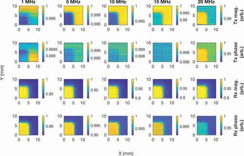
Figure 17. Normalised experimental results for notch 2 from the driving and receiving coils. The bottom and left labels are for the x-axis and y-axis respectively. The plots are organised into columns of the same frequency, given by the labels on the top edge. The plots are organised into rows according to the variable being measured as labelled on the right edge. Mag. is short for magnitude. The coils are on the sample in the bottom left corner.
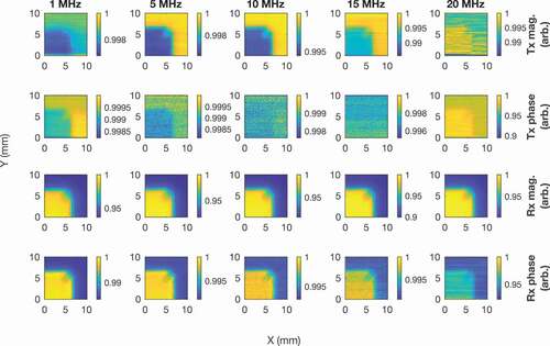
Figure 18. Normalised experimental results without notch from the driving and receiving coils. The bottom and left labels are for the x-axis and y-axis respectively. The plots are organised into columns of the same frequency, given by the labels on the top edge. The plots are organised into rows according to the variable being measured as labelled on the right edge. Mag. is short for magnitude. The coils are on the sample in the bottom left corner.
Again, a similar calculation for the SNR is used as seen in , but for the corner notch results. The search region for the defect is taken to be [3, 4, 2, 2] and the background region is taken to be [1, 4, 2, 2] for notch 1. For notch 2, the search region is taken to be [4, 4, 2, 2] while the background region is the same as before. One should again use caution as this is just intended to give a quantifiable and easy to obtain indicative value that could be used when repeating the experiments. The SNRs from this calculation is shown in .
The data for both notch 1 and 2 show similar behavior, though notch 2 does generally have a bigger SNR as the defect is larger. For these notches, the noise seems to be larger than that observed for the edge defects. Again, as for the edge defect, the SNR of the Tx phase measurement appears to decrease with frequency, but it can also be seen that the Rx phase measurement SNR just seems to decrease with frequency. This decrease in SNR in the phase data is evident in the scans, but this may just be caused by it being more difficult to measure small-phase differences at higher frequencies, particularly for the Tx coil.
The Rx mag. SNR seems to increase with frequency, benefitting from the increased localisation of the eddy current and thus signal at higher frequencies. While the Tx mag. SNR appears to increase initially, being optimal around 10 MHz, before the noise starts to dominate. This is evident in the scan, where the signal looks sharpest around the mid-point of the frequencies shown for Tx mag. The 10 MHz to 15 MHz regions may be a good comprise for good SNR in the mag. measurements, although a multifrequency response may also be advantageous in future work. Small defects near the edge of the sample can be detected with this approach, but one needs to be careful with the analysis of the signals.
Choosing an appropriate cross-section on the corner defects is much more difficult than for the edge defect, as the corner defects are much smaller, but this is shown for Rx mag. and Rx phase on notch 2 in . Here, it can be seen that while the signal does not rise above the sample, as is the case for the edge defect, it is possible to see the remnants of this with, a small peak existing within the broader trough.
Figure 19. Normalised cross-sections through the notch 2 2D scan, where the line starts at (4,6) mm and ends at (6,4). Values are interpolated to have 100 points for each plot and the Rx phase is from median filtering the original 2D plot with a 3 × 3 neighbourhood. The key gives the frequency in MHz. The 20 MHz result for the Rx phase is not shown, because the high noise present on that reading would obscure other results.
Modelling results for the defect on plate corner
show the simulation results for the notch defects, and modelling of the edge without a defect is shown in for comparison. The figures are normalised, but show the absolute values for each respective scan before normalisation. As for the edge defects, the absolute Tx mag. and Rx mag. values in agree with the experimental results presented in , with the magnitude and the general trend of these values increasing with frequency, which is seen in the experimental results. The exact values would not be expected to be the same as the modelled system is idealised. And again, it makes less sense to compare the experimental and modelled absolute values of the phase data, as the phase is compared to the function generator in the experiment, rather than the current, as is the case for the simulation.
Figure 20. Simulation results for 2D scans on titanium around notch 1 at varying frequencies. The bottom and left labels are for the x-axis and y-axis respectively. The plots are organised into columns of the same frequency, given by the labels on the top edge. The plots are organised into rows according to the variable being measured as labelled on the right edge. The label mag. is short for magnitude. The centre of the pair of coils and the sample corner coincide at (0,0) mm.
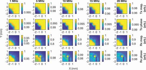
Figure 21. Simulation results for 2D scans on titanium around notch 2 at varying frequencies. The bottom and left labels are for the x-axis and y-axis respectively. The plots are organised into columns of the same frequency, given by the labels on the top edge. The plots are organised into rows according to the variable being measured as labelled on the right edge. The label mag. is short for magnitude. The centre of the pair of coils and the sample corner coincide at (0,0) mm.
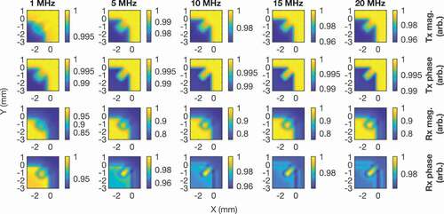
Figure 22. Simulation results for 2D scans on titanium without notch at varying frequencies. The bottom and left labels are for the x-axis and y-axis respectively. The plots are organised into columns of the same frequency, given by the labels on the top edge. The plots are organised into rows according to the variable being measured as labelled on the right edge. The label mag. is short for magnitude. The centre of the pair of coils and the sample corner coincide at (0,0) mm.
The defects are modelled as rectangular slots based on the width, depth and lengths measured optically. As such the features are larger and sharper than the notches made, but nevertheless, they are included for consistency and to help understand the behaviour of the defects with the eddy current sensor. Features that are seen in results for the edge defects would also be expected in the corner defects if the corner defects were also rectangular slots, such as the defect signal rising compared to both the sample and off-sample regions for the Rx phase at the higher frequencies. This, however, is not observed for the experimental results with the defects in the sample corner, perhaps because of the increased noise in the experimental results, or because the defects on the corners are more crudely made. That being said, there are similarities in the morphology of the general response to the defect.
Conclusion
The use of high-frequency, small diameter eddy current sensors with small coils of less than 1 mm in diameter enable one to clearly identify slot-like, simulated defects down to 1 mm in length, with reasonable SNRs. Small defects near the edge of a sample are notoriously difficult to detect due to the influence of the sample edge on the signal and this method provides a suitable method for finding defects close to the edge of even poorly electrically conducting samples such as titanium.
The quantitative measurement of the phase and mag. of the generation and detection coil simultaneously gives improved confidence in the detection of defects and indeed by combining these results, one can get improvements to the experimentally measured SNR. What is particularly striking though, is that the phase of the signal on the detection coil gives the highest resolution of defect shape and the most reliable result for distinguishing the simulated defect from the sample edge. This general behaviour was mirrored by simulation, where the simulation and experimental results were in good agreement, especially for notches at the edges of the sample.
For the particular coils and electronics used in this experiment, the optimum measurement was typically obtained at around 10 MHz, providing good SNRs. We have shown that using an eddy current transmit-receive coil pair at high frequencies, it is possible to detect very small defect like features close to the edge of a titanium sample with a good SNR, and that it is important to ensure that not only the mag. of the signal is measured on the detection coil, but also its phase.
Similar benefits may be expected with a different alignment of the T/R coils and notch, which could be something to consider for further work. Other avenues may include controlling lift-off, as high-frequency measurements may be affected more by lift-off.
Acknowledgements
I would like to acknowledge EPSRC for the DTA, RCNDE for the studentship, and Rolls Royce and EDF for sponsoring my PhD project. Also, thank you to Robert Day and David Greenshields for help with the electronics, and Jonathan Harrington for the mechanical advice and assistance.
Disclosure statement
No potential conflict of interest was reported by the author(s).
Data availability statement
The data that support the findings of this study are available from authors upon reasonable request https://warwick.ac.uk/fac/sci/physics/research/ultra/research/ced22.zip.
Additional information
Funding
References
- Yamada M. An overview on the development of titanium alloys for non-aerospace application in Japan. Mater Sci Eng A. 1996;213(1):8–15.
- Cooper SP, Whitley GH. Titanium in the power generation industry. Mater Sci Technol. 1987;3(2):91–96.
- Hu YN, Wu SC, Withers PJ, et al. The effect of manufacturing defects on the fatigue life of selective laser melted Ti-6Al-4V structures. Mater Des. 2020;192:108708.
- Bray DE, McBride D. Nondestructive testing techniques. John Wiley & Sons; 1992.
- Arias I, Achenbach JD. A model for the ultrasonic detection of surface-breaking cracks by the scanning laser source technique. Wave Motion. 2004;39(1):61–75.
- Geng L, Wen Y, Zhang F, et al. Machine vision detection method for surface defects of automobile stamping parts. American Scientific Research Journal for Engineering, Technology, and Sciences (ASRJETS). 2019 Mar 4. 53. 1. 128–144
- Ghoni R, Dollah M, Sulaiman A, et al. Defect characterization based on eddy current technique: technical review. Adv Mech Eng. 2014;6:182496.
- Sharma S, Elshafiey I, Udpa L, et al. Finite element modeling of eddy current probes for edge effect reduction. In: Thompson DO, Chimenti DE, editors. Review of progress in quantitative nondestructive evaluation. Vol. 16A. Boston (MA): Springer; 1997. p. 201–208.
- Xie Y, Li J, Tao Y, et al. Edge effect analysis and edge defect detection of titanium alloy based on eddy current testing. Appl Sci. 2020;10(24):8796.
- Dogaru T, Smith ST. Edge crack detection using a giant magnetoresistance based eddy current sensor. Case Stud NondestrTest Eval. 2000;16(1):31–53.
- Wang Y, Bai Q, Du W, et al. Edge effect on eddy current detection for subsurface defects in titanium alloys. Proceedings of the 8th International Conference on Computational Methods, Guilin, China. 2017.
- Underhill PR, Krause TW. Eddy current analysis of mid-bore and corner cracks in bolt holes. NDT E Int. 2011;44(6):513–518.
- Wu YH, Hsiao CC. Reliability assessment of automated eddy current system for turbine blades. Insight-Non-Destructive Test Condition Monit. 2003;45(5):332–336.
- Eua-Anant N, Udpa L, Chao J. Morphological processing for crack detection in eddy current images of jet engine disks. In: Thompson DO, Chimenti DE, editors. Review of progress in quantitative nondestructive evaluation. Vol. 18A. Boston (MA): Springer; 1999. p. 751–758.
- Fava J, Ruch M. Design, construction and characterisation of ECT sensors with rectangular planar coils. Insight-Non-Destructive Test Condition Monit. 2004;46(5):268–274.
- Gardner WE. Improving the effectiveness and reliability of non-destructive testing. Elsevier. 2013;62.
- Hughes F, Day R, Tung N, et al. High-frequency eddy current measurements using sensor-mounted electronics. Insight-Non-Destructive Test Condition Monit. 2016;58(11):596–600.
- Pelkner M, Pohl R, Erthner T, et al. Eddy current testing with high-spatial resolution probes using MR arrays as receiver. In 7th International symposium on NDT in aerospace (Proceedings) 2015 (No. DGZfP-BB 156, pp. We -5); Breman, Germany. Deutsche Gesellschaft für Zerstörungsfreie Prüfung ev (DGZfP).
- Heuer H, Schulze MH. Eddy current testing of carbon fiber materials by high resolution directional sensors. Smart Materials, Structures and NDT in Aerospace, NDT in Canada; 2011 Nov 2; Montreal, Quebec, Canada.
- Klein G, Morelli J, Krause TW. Analytical model of the eddy current response of a drive-receive coil system inside two concentric tubes. NDT E Int. 2018;96:18–25.
- Yu Y, Gao K, Liu B, et al. Semi-analytical method for characterization slit defects in conducting metal by Eddy current nondestructive technique. Sens Actuators A. 2020;301:111739.
- May P, Zhou E, Morton D. Numerical modelling and implementation of ferrite cored eddy current probes. NDT E Int. 2007;40(8):566–576.
- Theodoulidis T, Bowler, Bowler JR. JR interaction of an eddy-current coil with a right-angled conductive wedge. IEEE Trans Magn. 2009;46(4):1034–1042.
- Bowler JR, Theodoulidis TP, Poulakis N. Eddy current probe signals due to a crack at a right-angled corner. IEEE Trans Magn. 2012;48(12):4735–4746.
- To A, Li Z, Dixon S. Improved eddy current testing sensitivity using phase information. Insight-Non-Destructive Test Condition Monit. 2021;63(10):578–584.