
ABSTRACT
Efficient pre-processing is essential to the mechanical recovery of waste printed circuit boards (WPCBs). In this work, a thermal shock pretreatment was utilized to damage the interface between metals and nonmetals of single-sided copper clad laminates (SSCCLs), which are usually employed as the base material of printed circuit boards (PCBs). The effects of three thermal shock treatment parameters—i.e., peak temperature, holding time, and thermal shock cycle times—on the adhesion strength of SSCCLs were evaluated by orthogonal experiments. Microstructures and peel resistance of SSCCLs before and after thermal shock were characterized by scanning electron microscopy (SEM) and 90° peel test, respectively. Our results showed that the impact of three major factors that influence liberation efficiency was in the sequence of peak temperature > shock cycle times > holding time. Furthermore, the optimal thermal shock level could be achieved when the peak temperature was 300°C with the soaking time of 30 min and three cycle times. In the meantime, the corresponding peel strength of the SSCCLs (0.065 N/mm) was sharply decreased by 94% in comparison with those without thermal shock treatment. The manual dismantling experimental data verified the good feasibility of the optimal thermal shock process, suggesting that the copper foil could be readily dismantled from the substrate by hand after pretreatment, with a successful separation rate of 100% and a peeling efficiency of ~ 30 seconds per piece. Therefore, the optimal thermal shock process could notably improve liberation of metals and nonmetals, which would be helpful for efficient recycling of WPCBs.
Implications: The interface between copper foil and laminate dielectric in a PCB can be weakened significantly via efficient thermal shock method. Thus, a good liberation could be achieved after thermal shock. In this work, a manual peeling of copper foil from the SSCCL substrates was achieved efficiently after optimal thermal shock pretreatment, confirming the feasibility of a shorter process of metal recovery from scrap SSCCLs without pulverization. The results will be useful for the pretreatment of recovery of the WPCBs.
Introduction
Waste printed circuits boards (WPCBs), as one of the most important E-wastes, have much higher concentration of valuable metals when compared with natural ores. How to recycle metals from WPCBs in a manner that is eco-friendly and efficient has been the focus of many researchers in recent years (Holgersson et al. Citation2018; Robinson Citation2009). Currently, the existing recycling techniques of WPCBs mainly include physical and mechanical technology (Cui and Forssberg Citation2003; Verma, Singh, and Basha Citation2018; Zhang and Forssberg Citation1997), hydrometallurgical processing (Li, Eksteen, and Oraby Citation2018; Wang et al. Citation2018; Xiu et al. Citation2019, Citation2018, Citation2017) and the pyro-metallurgical method (Wang et al. Citation2017). Among these processes, the physical and mechanical recycling techniques, which efficiently separate the metallic and nonmetallic fractions of waste PCBs, are mainly used to upgrade the contents of valuable materials of WPCBs that can prepare a richer and cleaner feed for pyro- and hydrometallurgical and other processes (Hadi et al. Citation2015; Sarvar, Salarirad, and Shabani Citation2015).
WPCBs are extremely complicated composite materials consisting of conductive metal materials, glass fiber reinforced epoxy resin, plastics and electronic components (ECs). The ECs are commonly recognized as hazardous materials, such as capacitors and batteries, etc. Dismantling of the ECs is the first step in the physical and mechanical recycling process; subsequently, the base boards without ECs will be subjected to the processes of shredding and crushing or physical separation, including magnetic separation, electrostatic separation, eddy current separation, flotation process, and density separation. Thus, the separation of metallic and nonmetallic materials will be completed (Ghosh et al. Citation2015; Kaya Citation2016). The purpose of crushing is to reduce the size of the base boards to a certain extent, thereby achieving the full liberation of metals from nonmetals and subsequently making preparation for further separation. Zhang et al. (Citation2017) found that metal and nonmetals could be liberated favorably when the PCBs particle was less than 1.4 mm. Guo et al. (Citation2011) studied the liberation characteristic of PCBs, and the results showed that the metal and nonmetal particles of PCBs could be dissociated completely under a crush size of 0.6 mm using a two-step crushing process. Kaya (Citation2016) pointed out that pulverizing the PCBs to small sizes below 500 μm is necessary for reliable liberation. It can be seen that the physical liberation of base boards is mainly achieved by cumulative application of shredding and crushing, but the crushing process is an energy-intensive process accompanied by inevitable noise pollution.
Proper thermal pretreatment can be used for improving the liberation of metals and nonmetals during crushing due to the thermal properties’ mismatch between laminates inside PCBs. It has been confirmed that using a thermal pretreatment before crushing can significantly reduce energy consumption and noise pollution of the whole liberation (Chen et al. Citation2011; Duan Citation2010; Li et al. Citation2010a). Zhou et al. (2016) discussed low-temperature modification of discarded printed circuit board, revealing that the PCBs’ mechanical properties decreased significantly under the condition of cryogenic treatment at −20°C, which supported subsequent crushing and improved the recovery efficiency. However, these could cause an inconvenient operation and serious dust pollution. In addition, Li et al. (2010b) studied the impact of the peak temperature of thermal shock treatment on the interfacial and mechanical property of WPCBs; they found that the delaminating strength of PCBs could be reduced by 58.5% at 250°C compared with those of untreated ones, and the reduction of energy consumption and noise was 41.7% and 8.2% (dB) during crushing, respectively.
Many researchers (Ai, Fu, and He et al. Citation2015; Dong et al. Citation2017; Wang, Wang, and Dong et al. Citation2013) revealed that alternate heating and cooling composite materials could lead to laminates’ effective failure. During thermal treatment, besides peak temperature, both the holding time at peak temperature and thermal shock cycle times would exert a non-negligible influence on interface damage during thermal pretreatment. However, the impact of cycle times during thermal shock pretreatment on recovery of WPCBs has been rarely reported. Therefore, in order to reduce the delaminating strength of PCBs and to liberate metal and nonmetallic materials readily, a comprehensive study is encouraged to investigate the thermal shock process parameters.
In this work, taking standard single-sided copper clad laminates (SSCCLs) as the object of study, the main focus is on investigating the effect of peak temperature, thermal shock cycle times, and holding time at peak temperature on the adhesion strength of interfaces between copper foil and substrate materials. Orthogonal experiments were adopted to obtain an optimal thermal shock process. Orthogonal experimental design technique is an economical experimental design with high efficiency, which has been widely used to evaluate the effects of various factors on performance (Han, Tian, and Song et al. Citation2013; Li and Hao Citation2018). In addition, a group of manual dismantling experiments after thermal shock were applied to validate the feasibility and efficiency of delamination of SSCCLs.
Materials and methods
Standard single-sided copper clad laminates (SSCCLs) with an average copper foil thickness of 35 μm for flame retardant PCB (Model: FR-4 PCB) were used in this study. The SSCCL specimens for peeling strength test were prepared according to GB/T 4722–92; the sample size was 50 mm × 75 mm × 1.5 mm, with four pieces of parallel copper foils (3 mm × 75 mm × 35 μm) adhering to the reinforced matrix.
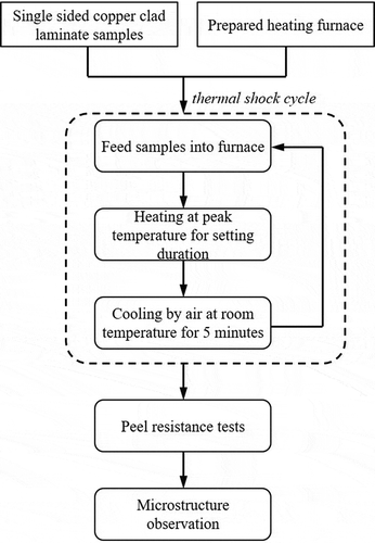
A thermo gravimetric analyzer (STA449C, NETZSCH) was utilized to analyze the SSCCLs in a temperature range from 25°C to 850°C with a rate of 10°C min−1. A thermal treatment furnace (BTF-1200C, AnHui BEQ Equipment Technology Co., Ltd., Hefei) was used for thermal shock treatment, equipped with a thermostat to control the inside temperature of the furnace with ±2°C error range (). The tube size was Φ60 mm × 800 mm, the heating zone length was 440 mm, and the constant temperature zone length was 200 mm. There are three steps during each thermal shock cycle: first, heating up the tube furnace to peak temperature; second, feeding SSCCL specimens quickly into the constant temperature zone of the tube furnace with a quartz boat, and then holding for a certain time; third, taking samples out of the furnace and cooling them down to room temperature in air for five minutes, And then starting the next cycle of thermal shock. Note that there is little temperature fluctuation during thermal shock; in the first two minutes, the inside of the furnace temperature is slightly lower (~ 5°C) than the setting temperature. This loss is caused by the feeding sample procedure. All thermal shock was carried out under air atmosphere in this study. The flow chart of the thermal shock processing is shown in .
Figure 1. Schematic diagram of the tubular furnace.
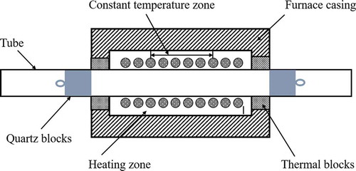
Figure 2. Flow chart of the thermal shock treatment.
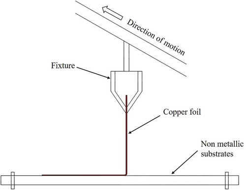
An orthogonal L9 (34) test was designed to study the influence of three parameters—peak temperature, thermal shock cycle times, and holding time (listed in )—on the adhesion strength of the interfaces of metals and nonmetals for SSCCLS. A 90° peel tester (shown in ) was used to measure the peel strength to evaluate the adhesion property of SSCCLs according to GB/T 4722–92. For each group of peeling strength tests, three pieces of SSCCL specimens were tested to obtain average value. The microstructural evolution of the interfaces was characterized by a scanning electron microscope (SEM, Quanta 200). Additionally, a manual dismantling experiment was carried out after thermal shock; the SSCCLs sample size for dismantling was 25 mm × 45 mm × 1.5 mm.
Table 1. Factors and levels of orthogonal experiments.
Figure 3. Schematic diagram of the peel tester.
Results and discussion
Structure and TGA of SSCCLs
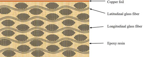
represents the cross-sectional macro-structural schematic of the SSCCLs. It is obvious that the SSCCLs are composed of three different laminates; i.e., copper foil used as conductive material, reinforced fabric woven by longitudinal and latitudinal glass fiber, and the epoxy resin with crosslinking agent as the non-conductive substrate and the binder role.
Figure 4. Cross-sectional macro-structural schematic of the SSCCL.
Thermo gravimetric analysis (TGA) was performed in both argon and air atmosphere in the temperature range of 25–850°C with a heating rate of 10°C min−1. As the TG samples were very small (less than 20 mg), in order to get reliable TGA data of SSCCLs, the SSCCL was first cut into little pieces (2 mm × 2 mm). The pieces with a weight of 15 (±2) mg were ground into powder as the TGA sample. The pieces’ structures are identical to that of SSCCL, and thus the obtained TGA data could guarantee the representation of SSCCLs.
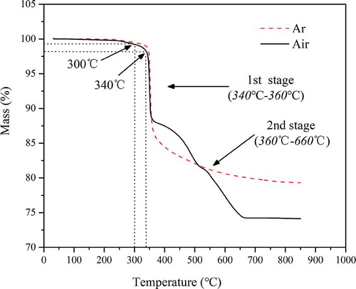
The TGA curve of SSCCL is shown in . It can be seen that when the temperature was below 300°C, the mass losses were very similar in argon and air atmosphere. The weight of SSCCLs reduced slightly, and the mass loss was less than 0.8%, which was attributed to the vaporization of moisture. In PCB laminates, the water can enter a microscopic interstitial void between the glass fibers and the epoxy resin matrix during synthetic and storage processes, and the transformation of water into vapor, along with increasing temperature, caused the slight mass loss. When the temperature was increased from 300°C to 340°C, the mass loss in air was only ~1.5%, which was caused by the volatile decomposition of additives such as curing accelerators in epoxy resin. When the temperature was higher than 340°C, the significant mass loss of SSCCLs occurred either in the argon atmosphere or in the air atmosphere (see ). The TG curve under argon atmosphere was relatively flat, indicating that the SSCCLs decomposed slowly when the temperature was higher than 400°C, while there are two distinct weight loss stages in air atmosphere. The weight loss of the first stage was ~ 10.9% in the temperature range of 340 ~ 360°C, and the second stage of weight loss was ~ 13.8% in the temperature range of 360 to 660°C; about 75.3 wt.% of SSCCLs was left. The difference with that under the inert atmosphere should be caused by the combustion of epoxy in an oxidized atmosphere (Smith Citation2016). Similar results were reported in previous studies with regard to the pyrolysis of PCB using TGA and Fourier transformation infrared (FTIR) integrated analysis (Alenezi and Al-Fadhli Citation2018; Barontini et al. Citation2005; Du et al. Citation2018; Guo et al. Citation2010; Li et al. Citation2010a; Zhao, Zhang, and Shi Citation2017), and their detailed results are summarized in . To minimize environmental influence during the degradation of SSCCLs, as for thermal shock treatment in this study, the appropriate temperature for treating SSCCLs should not be higher than 300°C, which is consistent with a series of temperatures in the designed orthogonal experiments (seen in ).
Table 2. Pyrolysis of scrap PCBs analyzed by a number of publications.
Figure 5. TGA curves of the SSCCL.
Peel resistance based on orthogonal thermal shock experiment
Peel resistance has to fit industry standards during production, since it is an important property for copper clad laminates. During the thermal shock, peel resistance was chosen as a key indicator due to its critical impact on the dissociation of metallic and nonmetallic materials.
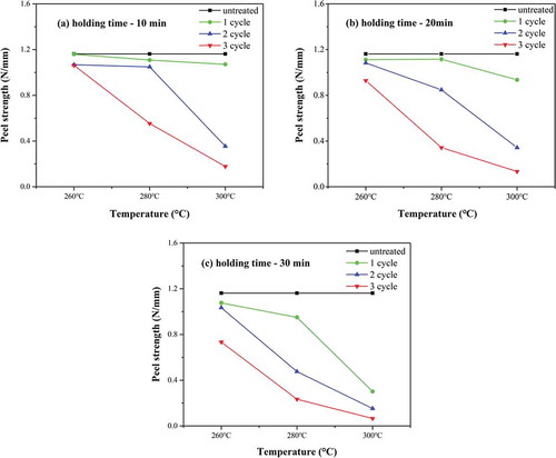
Peel resistance of these SSCCLs after thermal shock treatment was measured based on orthogonal experiments. There were 12 peel strength data samples for each group of SSCCL specimens. The maximum and minimum values were excluded; the average value of the 10 values left was the final data shown in results. The deviation between 10 values in each group was less than 0.15 N/mm. The results are summarized in . As shown in , K1, K2, and K3 represent the sum of the peel strengths corresponding to the three levels of each factor. R represents the difference range of the peel strength of the SSCCLs corresponding to the three levels of each factor, R = max (K1, K2, K3) – min (K1, K2, K3). The influence trend of each factor on the peel strength is illustrated in . It is shown from extreme difference analysis of peel resistance () that the peak temperature is the most important factor, and the importance is reduced in the order of shock cycles and then holding time. The combination of the best thermal shock condition obtained from is A3B3C3; i.e., peak temperature at 300°C, holding time of 30 min, and three cycle times. Since the A3B3C3 condition did not exist in the nine series of the orthogonal experiments, it is necessary to carry out sufficient thermal shock experiments for further verification. The effect of peak temperature, holding time, and shock cycles on peeling strength is shown in . It can be seen that peel strength decreases as the peak temperature, cycle times, and holding period increase. Results of A3B3C3 showed that the corresponding peel resistance of the SSCCLs was 0.065 N/mm, which was sharply decreased by 94% compared with untreated samples (1.162 N/mm). Meanwhile, the peel resistance of SSCCLs for the No. 8 experiment (A3B2C3) in was decreased by 86%, and the weight loss was ~ 4.5% under A3B3C3 condition, without obvious decomposition of epoxy resin. If the SSCCL was heated under continuous condition at 300°C for 90 min without cooling, the weight loss was ~10%, which is significantly higher than that of the intermittent condition (A3B3C3); in addition, an obvious pungent smell was released, caused by the accumulation of heat energy. Therefore, the thermal shock should not be applied at temperatures higher than 300°C with continuous times longer than 30 min per cycle, as this may lead to a severe decomposition process. Thus, the combination of optimal thermal shock condition obtained is A3B3C3 for SSCCLs.
Table 3. The factional factorial experiments.
Figure 6. Peel strength trend under different shock conditions.
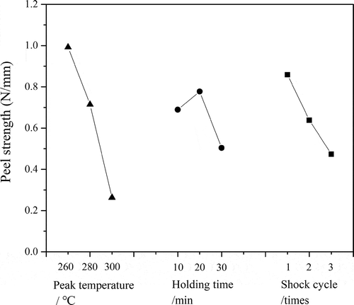
Figure 7. The effect of peak temperature, holding time, and shock cycles on peeling strength.
Microstructures of the SSCCLs after thermal shock
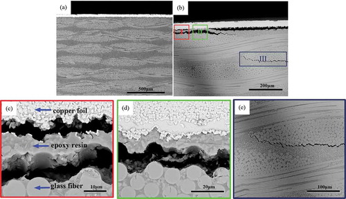
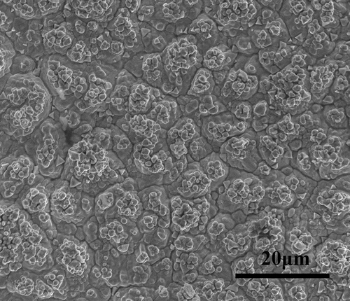
illustrates the microstructure of SSCCLs before and after thermal shock treatment under the optimal condition (300°C, 30 minutes, three cycle times). As shown in , a clear laminated structure and tight crosslinking between copper foil, glass fiber, and epoxy resin can be seen in untreated SSCCLs. As shown in , when the interface between copper foil and nonmetal matrix was evidently destroyed, three types of interfacial failure, marked with square frames in red (I), green (II), and blue (III) colors, respectively, were generated. In area I (), epoxy resin was delaminated from both copper foil and glass fiber. In area II (), epoxy resin was separated from glass fiber, but still adhered to copper foil. In area III (), interfacial failure between epoxy and glass fiber inside the nonmetal matrix was observed.
Figure 8. Microstructure of the interface of metals and nonmetals for SSCCLs before and after thermal shock: (a) untreated SSCCLs, (b) treated SSCCLs, (c–e) enlarged drawings corresponding to area I, II, and III in (b), respectively.
The interface bonding failure among the layers in copper clad laminates by thermal shock treatment results from a combination of various stresses. Since SSCCLs are anisotropic materials, the coefficients of thermal expansion (CTE) of copper foil, epoxy resin, and glass fiber are quite different in the x, y, and z axes. Note that the z axis represents the thickness direction of laminate. The linear CTEs for common copper foil, epoxy resin, and E-glass fiber are 16.7, approximately 15–100, and 54 parts per million (ppm)/°C, respectively (Li et al. Citation2010b). Additional studies have revealed that the CTE value of the glass fiber in a radial direction was approximately 5 ppm/°C, while that of unreinforced epoxy resin can range from 50 to 65 ppm/°C (Sood and Pecht Citation2018; Zhu, Shrotriya, and Sottos et al. Citation2003). Sottos et al. investigated the thermo elastic properties of woven glass/epoxy substrates using thermal mechanical analysis (TMA); they found that the expansion is linear and the CTE nearly constantly below the glass transition (Tg). At 100°C, the expansion becomes nonlinear and the CTE increases rapidly, reaching a maximum at ~ 125°C. After this peak temperature, the expansion drops quickly to a value lower than that of room temperature (Sottos, Ockers, and Swindeman Citation1999). Furthermore, Duan (Citation2010) pointed out that the modulus was also different in the x, y, and z axes (Duan Citation2010). The modulus of polymer is more dynamics, depending on the temperature. As such, thermal stress among the layers can be accumulated during the alternation of heating and cooling. In addition, as epoxy resin is heated, it can undergo a second-order thermodynamic transition from a glassy solid into a rubbery material. The glass transition temperature (Tg) of epoxy resin is approximately 170°C or less (Polansky´ et al. Citation2009; Smith Citation2016). When the temperature is higher than 170°C, epoxy resin transforms from a glassy state into a rubbery one, and the modulus decreases abruptly. Moreover, during the cooling of the materials, the transition is reversible, revealing that it can also occur in the opposite direction. The transformation stress existed among the laminates. Due to the apparently different wet expansion coefficients of the laminate materials, the phenomenon of wet stress concentration occurs at the interface among the laminates. The moisture can be naturally absorbed onto the SSCCLs. In the process of rapid heating, the internal moisture inside the SSCCLs will rapidly transform into steam, favoring the liberation of the interfaces. Since the SSCCLs were processed and synthesized at a certain temperature, thermal residual stress will exist in the fiber, the matrix, and the interface layer during the cooling process, thereby leading to a great impact on the properties of fiber reinforced composites (Zeng et al. Citation2013). In the process of manufacturing SSCCLs, the copper foil surface should be roughened before being bonded onto the substrate, with the aim of generating a strong bonding force to form an anchoring effect. Once the total internal stresses overcome the interface bonding strength of the material during thermal shock treatment, a crack will be formed and the delamination of SSCCLs will finally occur.
Manual peeling after thermal shock
Peel strength decreases remarkably as both the thermal temperature and shock cycles increase, and it’s feasible to liberate the copper foil from the substrates manually. Thus, experiments were carried out to validate the feasibility of optimal thermal shock parameters.
The results of the manual peeling verification procedure are shown in . All samples were peeled manually after thermal shock treatment under the optimal condition (300°C, 30 minutes, three cycle times). The success rate of manual peeling copper foil was 100%, and the efficiency of manual peeling was ~ 30 seconds per piece of sample. The surface appearance of copper foil after manual peeling is shown in ; the roughening processed surface is clean only with a small amount of adhesives. Accordingly, the separation of copper foil and substrates of SSCCLs can be achieved directly. Although the structure of SSCCLs is simpler than that of PCBs, thermal shock should be a good pretreatment to weaken the interface between metal and nonmetal, which should be helpful for the recovery process of WPCBs. In addition, as the thermal treatment temperature is higher than the melting point of the welding solder (normally less than 200°C), suitable thermal shock pretreatment probably could be applied to the electric components releasing from the WPCBs.
Figure 9. Manual peeling verification procedure under the optimal thermal shock condition.
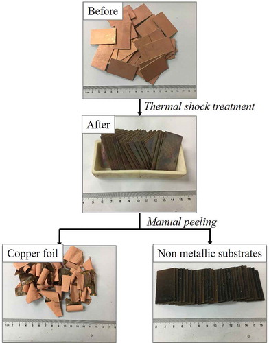
Figure 10. Copper foil surface after manual peeling.
Further processing suggestion after thermal shock
As the copper foil could be easily peeled off, four methods could be feasible for further processing: (1) applying rolling devices and air bed separation to separate copper foil and nonmetallic matrix automatically, so that the copper foil can be easily recycled after being bathed to remove the discolored surface and slight adhesiveness; (2) leaching the treated laminates with organic solvent for complete separation; previous studies have shown that solvents such as dimethyl sulfoxide solvent (DMSO), dimethylformamide (DMAc), N-methyl-2-pyrrolidone (NMP), and dimethylfomamide (DMF) were helpful for dismantling the copper from nonmetallic substrates (Verma, Singh, and Mankhand Citation2017a, Citation2017b, Citation2017c; Wath et al. Citation2015; Zhu et al. Citation2013a, Citation2013b); as the interface was already weakened by the pre-process, leaching efficiency could be improved accordingly; (3) Li et al. (Citation2010b) found that comparing with crushing directly to liberate metallic and nonmetallic of WPCBs, the thermal pretreatment process could significantly reduce energy consumption and noise (Li et al. Citation2010b); thus, crushing should also be a potential further processing method following thermal shock.
Conclusion
In this paper, the effects of a thermal shock process on the microstructure and peel resistance of the interface of copper foil and nonmetallic matrix for SSCCLs were investigated. The following conclusions have been drawn:
1. The orthogonal experiment results showed that the importance of processing parameters was reduced in the order of peak temperature, shock cycles, and holding time. The combination of the best thermal shock condition obtained is listed as follows: peak temperature at 300°C, 30 minutes as holding time, and three cycle times.
2. Thermal shock can effectively weaken the bonding strength between the copper foil and the substrate. The corresponding peel strength of the SSCCLs (0.065 N/mm) was sharply decreased by 94% compared to those of the untreated samples.
3. A 100% successful manual separation of metals and nonmetals of SSCCLs was achieved, confirming the feasibility of thermal shock treatment.
Additional information
Funding
Notes on contributors
Fangfang Liu
Fangfang Liu is a Ph.D. student at the Guangdong Key Laboratory for Advanced Metallic Materials Processing, South China University of Technology, in Guangzhou, People’s Republic of China, and a lecturer at Dongguan University of Science and Technology, in Dongguan, People’s Republic of China.
Bingbing Wan
Bingbing Wan is a postdoctoral researcher at the School of Materials Science and Engineering, Dongguan University of Technology, Dongguan, People’s Republic of China.
Fazhan Wang
Fazhan Wang is a master’s student at the Guangdong Key Laboratory for Advanced Metallic Materials Processing, South China University of Technology, Guangzhou, People’s Republic of China.
Weiping Chen
Weiping Chen is a distinguished professor at Guangdong Key Laboratory for Advanced Metallic Materials Processing, South China University of Technology, Guangzhou, People’s Republic of China.
Related Research Data
References
- Ai, S., H. Fu, R. He, and Y. Pei. 2015. Multi-scale modeling of thermal expansion coefficients of C/C composites at high temperature. Mater. Des. 82:181–88. doi:10.1016/j.matdes.2015.05.061.
- Alenezi, R. A., and F. M. Al-Fadhli. 2018. Thermal degradation kinetics of waste printed circuit boards. Chem. Eng. Res. Des. 130:87–94. doi:10.1016/j.cherd.2017.12.005.
- Barontini, F., K. Marsanich, L. Petarca, and V. Cozzani. 2005. Thermal degradation and decomposition products of electronic boards containing BFRs. Ind. Eng. Chem. Res. 44 (12):4186–99. doi:10.1021/ie0487661.
- Chen, Y., J. Li, H. Duan, and Z. Wang. 2011. Thermal cracking of waste printed wiring boards for mechanical recycling by using residual steam preprocessing. Front. Environ. Sci. Eng. China 5 (2):167–74. doi:10.1007/s11783-011-0308-4.
- Cui, J., and E. Forssberg. 2003. Mechanical recycling of waste electric and electronic equipment: A review. J. Hazard. Mater. B99:243–63. doi:10.1016/S0304-3894(03)00061-X.
- Dong, K., X. Peng, J. Zhang, B. Gu, and B. Sun. 2017. Temperature-dependent thermal expansion behaviors of carbon fiber/epoxy plain woven composites: Experimental and numerical studies. Compos. Struct. 176:319–41. doi:10.1016/j.compstruct.2017.05.036.
- Du, N., H. Ma, X. Lin, J. Zhang, and C. Liu. 2018. Experimental investigation on the heat transfer characteristics in process of printed circuit boards pyrolysis under nitrogen flow. Sci. Total Environ. 636:1032–39. doi:10.1016/j.scitotenv.2018.04.365.
- Duan, H. 2010. Recycling of waste printed wiring board subjected to thermal preprocessing and its influencing mechanism. Dissertation for Doctor Degree. Beijing: Tsinghua University (in Chinese).
- Ghosh, B., P. Parhi, P. S. Mukherjee, and B. K. Mishra. 2015. Waste printed circuit boards recycling: An extensive assessment of current status. J. Clean. Prod. 94:5–19. doi:10.1016/j.jclepro.2015.02.024.
- Guo, C., H. Wang, W. Liang, J. Fu, and X. Yi. 2011. Liberation characteristic and physical separation of printed circuit board (PCB). Waste Manag. 31:2161–66. doi:10.1016/j.wasman.2011.05.011.
- Guo, Q., X. Yue, M. Wang, and Y. Liu. 2010. Pyrolysis of scrap printed circuit board plastic particles in a fluidized bed. Powder Technol. 198:422–28. doi:10.1016/j.powtec.2009.12.011.
- Hadi, P., M. Xu, C. S. K. Lin, C. Hui, and G. Mckay. 2015. Waste printed circuit board recycling techniques and product utilization. J. Hazard. Mater. 283:234–43. doi:10.1016/j.jhazmat.2014.09.032.
- Han, C., B. Tian, J. Song, and Z. Hou. 2013. Based on the orthogonal design to study the design and optimization of material composition for curing compound. Adv. Mater. Res. 857:124–29. doi:10.4028/www.scientific.net/amr.857.124.
- Holgersson, S., B. M. Steenari, M. Björkman, and K. Cullbrand. 2018. Analysis of the metal content of small-size Waste Electric and Electronic Equipment (WEEE) printed circuit boards—Part 1: Internet routers, mobile phones and smartphones. Resour. Conserv. Recycl. 133:300–08. doi:10.1016/j.resconrec.2017.02.011.
- Kaya, M. 2016. Recovery of metals and nonmetals from electronic waste by physical and chemical recycling processes. Waste Manag. 57:64–90. doi:10.1016/j.wasman.2016.08.004.
- Li, H., J. Eksteen, and E. Oraby. 2018. Hydrometallurgical recovery of metals from waste printed circuit boards (WPCBs): Current status and perspectives – A review. Resour. Conserv. Recycl. 139:122–39. doi:10.1016/j.resconrec.2018.08.007.
- Li, J., H. Duan, K. Yu, L. Liu, and S. Wang. 2010a. Characteristic of low-temperature pyrolysis of printed circuit boards subjected to various atmosphere. Resour. Conserv. Recycl. 54:810–15. doi:10.1016/j.resconrec.2009.12.011.
- Li, J., H. Duan, K. Yu, and S. Wang. 2010b. Interfacial and mechanical property analysis of waste printed circuit boards subject to thermal shock. J. Air Waste Manage. Assoc. 60:229–36. doi:10.3155/1047-3289.60.2.229.
- Li, X., and J. Hao. 2018. Orthogonal test design for optimization of synthesis of super early strength anchoring material. Constr. Build. Mater. 181:42–48. doi:10.1016/j.conbuildmat.2018.06.029.
- Polansky´, R., V. Mentlı´k, P. Prosr, and J. Susˇı´r. 2009. Influence of thermal treatment on the glass transition temperature of thermosetting epoxy laminate. Polym Test 28:428–36. doi:10.1016/j.polymertesting.2009.03.004.
- Robinson, B. H. 2009. E-waste: An assessment of global production and environmental impacts. Sci. Total Environ. 408 (2):183–91. doi:10.1016/j.scitotenv.2009.09.044.
- Sarvar, M., M. M. Salarirad, and M. A. Shabani. 2015. Characterization and mechanical separation of metals from computer Printed Circuit Boards (PCBs) based on mineral processing methods. Waste Manag. 45:246–57. doi:10.1016/j.wasman.2015.06.020.
- Smith, C. A. 2016. Thermochemical and physical properties of printed circuit board laminates and other polymers used in the electronics industry. Polym Test 52:234–45. doi:10.1016/j.polymertesting.2016.04.017.
- Sood, B., and M. Pecht. 2018. The effect of epoxy/glass interfaces on CAF failures in printed circuit board. Microelectron. Reliab. 82:235–43. doi:10.1016/j.microrel.2017.10.027.
- Sottos, N. R., J. M. Ockers, and M. Swindeman. 1999. Thermo elastic properties of plain weave composites for multilayer circuit board applications. J. Electron. Packag. 121 (1):37–43. doi:10.1115/1.2792659.
- Verma, H. R., K. K. Singh, and S. M. Basha. 2018. Effect of milling parameters on the concentration of copper content of hammer-milled waste PCBs: A case study. J. Sustainable Metall. 4:187–93. doi:10.1007/s40831-018-0179-z.
- Verma, H. R., K. K. Singh, and T. R. Mankhand. 2017a. Comparative study of printed circuit board recycling by cracking of internal layers using organic solvents-dimethylformamide and dimethylacetamide. J. Clean. Prod. 142:1721–27. doi:10.1016/j.jclepro.2016.11.118.
- Verma, H. R., K. K. Singh, and T. R. Mankhand. 2017b. Delamination mechanism study of large size waste printed circuit boards by using dimethylacetamide. Waste Manag. 65:139–46. doi:10.1016/j.wasman.2017.04.013.
- Verma, H. R., K. K. Singh, and T. R. Mankhand. 2017c. Liberation of metal clads of waste printed circuit boards by removal of halogenated epoxy resin substrate using dimethylacetamide. Waste Manag. 60:652–59. doi:10.1016/j.wasman.2016.12.031.
- Wang, H., S. Zhang, B. Li, D. Pan, Y. Wu, and T. Zuo. 2017. Recovery of waste printed circuit boards through pyro-metallurgical processing: A review. Resour. Conserv. Recycl. 126:209–18. doi:10.1016/j.resconrec.2017.08.001.
- Wang, L., Q. Li, Y. Li, X. Sun, J. Li, J. Shen, W. Han, and L. Wang. 2018. A novel approach for recovery of metals from waste printed circuit boards and simultaneous removal of iron from steel pickling waste liquor by two-step hydrometallurgical method. Waste Manag. 71:411–19. doi:10.1016/j.wasman.2017.10.002.
- Wang, L., Z. Wang, S. M. Dong, W. Zhang, and Y. Wang. 2013. Finite element simulation of stress distribution and development of Cf/SiC ceramic–Matrix composite coated with single layer SiC coating during thermal shock. Composites Part B: Eng. 51:204–14. doi:10.1016/j.compositesb.2013.03.028.
- Wath, S. B., M. N. Katariya, S. K. Singh, G. S. Kanade, and A. N. Vaidya. 2015. Separation of WPCBs by dissolution of brominated epoxy resins using DMSO and NMP: A comparative study. Chem. Eng. J. 280:391–98. doi:10.1016/j.cej.2015.06.007.
- Xiu, F., Y. Li, Y. Qi, X. Yu, J. He, Y. Lu, X. Gao, Y. Deng, and Z. Song. 2019. A novel treatment of waste printed circuit boards by low-temperature near-critical aqueous ammonia: Debromination and preparation of nitrogen-containing fine chemicals. Waste Manag. 84:355–63. doi:10.1016/j.wasman.2018.12.010.
- Xiu, F., Y. Qi, S. Wang, W. Nie, H. Weng, and M. Chen. 2018. Application of critical water-alcohol composite medium to treat waste printed circuit boards: Oil phase products characteristic and debromination. J. Hazard. Mater. 344:333–42. doi:10.1016/j.jhazmat.2017.10.033.
- Xiu, F., H. Weng, Y. Qi, G. Yu, Z. Zhang, F. Zhang, and M. Chen. 2017. A novel recovery method of copper from waste printed circuit boards by supercritical methanol process: Preparation of ultrafine copper materials. Waste Manag. 60:643–51. doi:10.1016/j.wasman.2016.11.001.
- Zeng, X., J. Li, H. Xie, and L. Liu. 2013. A novel dismantling process of waste printed circuit boards using water-soluble ionic liquid. Chemosphere 93:1288–94. doi:10.1016/j.chemosphere.2013.06.063.
- Zhang, G., H. Wang, Y. He, X. Yang, Z. Peng, T. Zhang, and S. Wang. 2017. Triboelectric separation technology for removing inorganics from non-metallic fraction of waste printed circuit boards: Influence of size fraction and process optimization. Waste Manag. 60:42–49. doi:10.1016/j.wasman.2016.08.010.
- Zhang, S., and E. Forssberg. 1997. Mechanical separation-oriented characterization of electronic scrap. Resour. Conserv. Recycl. 21 (4):247–69. doi:10.1016/S0921-3449(97)00039-6.
- Zhao, C., X. Zhang, and L. Shi. 2017. Catalytic pyrolysis characteristics of scrap printed circuit boards by TG-FTIR. Waste Manag. 61:354–61. doi:10.1016/j.wasman.2016.12.019.
- Zhou, C., Y. Pan, M. Lu, and C. Yang. 2016. Liberation characteristics after cryogenic modification and air table separation of discarded printed circuit boards. J. Hazard. Mater. 311:203–09. doi:10.1016/j.jhazmat.2016.03.008.
- Zhu, P., Y. Chen, L. Wang, G. Qian, W. Zhang, M. Zhou, and J. Zhou. 2013b. Dissolution of brominated epoxy resins by dimethyl sulfoxide to separate waste printed circuit boards. Environ. Sci. Technol. 47 (6):2654–60. doi:10.1021/es303264c.
- Zhu, P., Y. Chen, L. Wang, G. Qian, M. Zhou, and J. Zhou. 2013a. A novel approach to separation of waste printed circuit boards using dimethyl sulfoxide. Int. J. Environ. Sci. Technol. 10 (1):175–80. doi:10.1007/s13762-012-0124-9.
- Zhu, Q., P. Shrotriya, N. R. Sottos, and P. H. Geubelle. 2003. Three-dimensional viscoelastic simulation of woven composite substrates for multilayer circuit boards. Compos. Sci. Technol. 63 (13):1971–83. doi:10.1016/s0266-3538(03)00171-4.