
ABSTRACT
In this study, an algorithm for sorting waste products that is capable of automatically determining the value of raw materials during the sorting process is proposed. The algorithm automatically measures the sum of the top surface areas of integrated circuits (ICs), memory assemblies, and connectors (which account for over 80% of the resource value) from two-dimensional (2D) digital images of waste printed circuit boards. The sum of top surface areas is directly correlated with the total resource value. This algorithm continuously identifies the characteristics (e.g., color, size, and shape) of each device and performs relatively simple sequences of image processing. Tests on 46 types of waste digital-camera boards reveal the detection rates for ICs/memories and connectors to be 73% and 86%, respectively. The first measure is low because ICs/memories with long-side lengths of 2–5 mm are incorrectly identified as transistors or diodes in several cases. However, the proportion of ICs and memories with sides ≥5 mm is determined to be approximately 90% based on the sum of top surface areas, and the estimated values are 105% and 95% of the measured values, respectively. Furthermore, the sum of the top surface areas of both ICs and connectors is 101%. This reveals that the resource values can be estimated with a certain degree of accuracy. The analysis of cases of false detection and non-detection enable the identification of the major factors causing non-identification. The use of machine learning algorithms is determined to be an effective countermeasure. Furthermore, mitigation methods are specified.
Implications: An automatic detection algorism of electric devices mounted on waste printed circuit boards was constructed to straightforwardly and rapidly evaluate the resource values of printed circuit boards in small waste home appliances. A program developed based on the algorithm automatically measures the sum of the top surface areas of ICs/memory and connectors, which account for over 80% of the resource value of mounted devices. Because the structure of the algorithm is simple and can be applied to multiple target devices, high-speed processing can be achieved when implementing a waste product sorter.
Introduction
The recovery of valuable metals contained in waste electronic equipment has been identified as a highly effective and resourceful approach in Japan, where metal mines are few. The resource value of small waste household appliances is mostly related to their internal printed circuit boards. Therefore, it is important to understand their elemental compositions. In Japan, such waste resources are known as “urban mines.” Oki (Oki Citation2014) proposed the concept of strategic urban mining as a method to systematically develop a better resource-recycling society. The essence of this concept is that the arterial and venous industries can collaborate to realize sustainable and economically rational resource circulation. In addition, metal resources should be selected strategically and their potential values evaluated. Furthermore, physical separation processes that enable both cost reduction and sophistication, and hydrometallurgical processes that support a wide variety of small quantities have been developed by utilizing the waste-product information provided by the arterial industry.
The authors of this paper have been working on a national project since 2017 to develop a consistent automatic/autonomous control-type sorting system based on this concept. This system classifies waste materials from the circuit boards of small household appliances based on their resource value. This would enable the automatic regrouping of dismantled parts into raw materials for smelting. The innovative waste-product sorter enables the instantaneous identification of waste equipment based on a combination of individual recognition algorithms. One of these algorithms automatically identifies individual equipment types by reading product label information (Hayashi, Koyanaka, and Oki Citation2019). After this recognition process, resource-value evaluation and sorting can be realized by referring to a linked database. In this database, the composition, price, and other details of the material elements are registered as ranges of manufacturing year, structural information, disassembly process, and composition of parts.
Presently, major elements can be investigated using fluorescence X-ray analysis after circuit boards are crushed. However, for trace elements, time-consuming processes, such as inductively coupled plasma atomic emission spectrometry (ICP-AES) and mass spectrometry (ICP-MS), must be performed for each type of circuit board (Dervisevic et al. Citation2013). The innovative concept of this study is that a highly accurate automatic measurement of the type, size, and number of mounted devices from imagery can considerably simplify the process of identifying elemental compositions and sorting for recovery. Therefore, the aim of the work was to construct and verify an automatic detection algorithm for electronic devices that uses images of waste printed circuit boards.
Although several studies have evaluated circuit boards for elemental component recognition, few studies have systematically evaluated their composite values (Matsunaga et al. Citation2015). In one of these studies, Silva et al. (Silva et al. Citation2021) attempted to measure the top surface areas of ICs mounted on waste circuit boards to estimate their individual values by the YOLO algorithm (a type of deep learning network for object detection). This was aimed at the selection of a recycling process. In contrast, the automation of defect detection or positioning soldering by image recognition has been attempted for product management of electronic components. Hue, saturation, and luminance (HSL) methods can be used to identify materials based on their characteristic colors (Mogi, Namekawa, and Ueda Citation2012). Moreover, template-matching techniques involving device images can be used to identify materials by shape and organization (Chiah et al. Citation2012). Histograms of oriented gradient comparisons (Nishimura et al. Citation2018, Citation2019), dynamic programming methods that match pixel frequency distributions (Esaki et al. Citation2006), and multi-layer perceptrons that learn appearance shapes (Lefkaditis and Tsirigotis Citation2010) are also used for similar purposes. Furthermore, several methods using deep learning networks have been proposed recently. Typical ones use the YOLO algorithm (Adibhatla et al. Citation2020, Citation2021; Dai et al. Citation2020; Li et al. Citation2021; Ye et al. Citation2020). Improvements in the detection accuracy of various deep neural networks, including convolution layers, have also been attempted (Hu and Wang Citation2020; Li et al. Citation2021; Lian et al. Citation2021; Xia et al. Citation2021). Furthermore, it has become evident that a high detection accuracy can be achieved. However, because these methods are intended for specific product types, the target devices are limited, and images and appearance data can be obtained directly in advance. Moreover, many types of printed circuit boards are used in small household appliances, and the components mounted on these are diverse in type, size, shape, etc. This hinders the accurate detection of types and compositions.
In this study, we developed an algorithm that can rapidly detect device types and measure the sums of the top surface areas of components using two-dimensional (2D) digital image information (e.g., color, size, and shape) by combining relatively simple image processing. We clarified that it is sufficient to detect ICs and connectors among a wide variety of electronic elements mounted on waste printed circuit boards. The results reveal that the algorithm can be used as a value-based sorting standard for our national project. The subject is printed circuit boards mounted inside small household appliances, personal computers, and so on. But this time, as a representative, only waste digital-camera boards were targeted. Therefore, it should be noted that the results are limited to waste digital-camera boards. Herein, we present our observations that reveal that it is essentially difficult to further improve the detection accuracy. We also discuss the measures to be applied to achieve higher accuracy.
Analysis of resource value of waste digital-camera circuit boards
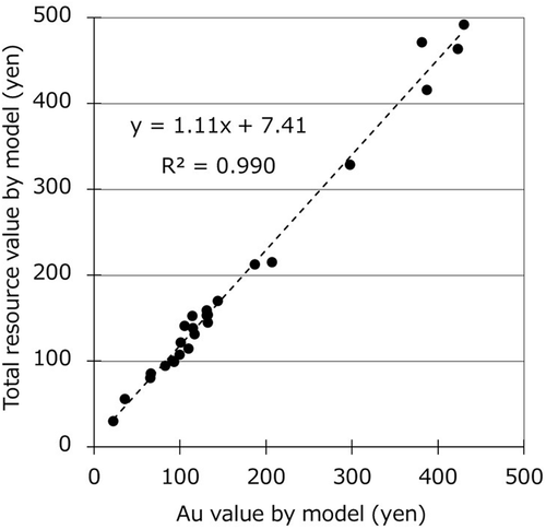
In this study, printed circuit boards of digital cameras were used as samples. This was because these are valuable, relatively common among small home appliances (Aizawa, Hirai, and Sakai Citation2009), and of a wide variety of types. First, to investigate the resource value of waste circuit boards, 26 waste digital-camera models manufactured by five domestic intermediate processing manufacturers between 2000 and 2014 were collected. The cameras were disassembled by hand. Multiple printed boards were removed, crushed with a small cutter mill, and heated in an air atmosphere (450°C, 4 h). Subsequently, fluorescence X-ray analysis, pressure acid decomposition (for trace-elemental analysis), ICP-AES, and ICP-MS were performed. The weight of each element obtained by the analysis was multiplied by the element price as of April 30, 2020 (MineralPrices.com Citation2020) to calculate the price of the circuit boards contained in each digital-camera model ($1 = ¥107.9; Au: ¥6,411/g; Ag: ¥56.8/g; Cu: ¥0.56/g; Ta: ¥16.4/g; Pd: ¥7207/g). shows the relationship between the value of Au per model and the total resource value per model. The total resource value varied between ¥30 and ¥492, with an average of ¥187. The plots are distributed almost on a straight line (correlation coefficient R2 (contribution rate) = 0.990) (Muto Citation1995). The slope of the regression line (1.11) reveals a strong positive correlation between the value of Au and the total resource value. Thus, even if the value of Au was assumed to be a uniform value of approximately 90.0% of the circuit boards of any value, there was almost no error in this value.
Figure 1. Relationship between Au value of board and total resource value per waste digital-camera model.
In addition, all the electronic devices mounted on 18 camera models obtained separately for verification were removed from the circuit boards. The weight ratio was measured for each device type, and the above elemental analysis was repeated. Based on the results of the elemental analysis, the Au concentration of each device and the proportion of Au contained in the circuit board when the device was mounted were calculated as distribution ratios, which are summarized in . The devices with a high weight ratio included Al electrolytic capacitors (19.3%), ports (9.3%), and IC/memory (8.6%). The circuit board portion without devices (i.e., glass epoxy resin circuit board + flexible circuit board) accounted for 33.8%. The devices with a high Au concentration were IC/memory (8,960 ppm), transistor/diode (5,500 ppm), and crystal oscillator (4,000 ppm). The IC/memory value was considerably high (66.0%) when converted to a distribution ratio considering the weight ratio, and was followed by the connector value (7.52%). Considering the distribution ratio of only devices (i.e., excluding the board part), the two types of IC/memory and connector exceeded 80%.
Table 1. Au distribution ratios for electronic devices mounted on waste digital-camera boards
The Au value depends on the number and size of the ICs/memories and connectors. Thus, we conjectured that the total resource value could be estimated by considering the total area of the top surfaces of the ICs, connectors, and ICs + connectors mounted on the board included in each of the 26 models and the relationships with the Au value per model, as shown in (a–c). Note that there were few ICs and connectors with long sides < 2 mm. These were considered to comprise a marginal proportion of the total top surface area. Therefore, items measuring ≥2 mm were the target of the investigation.
Figure 2. Relationship between the sum of the IC and connector top-surface areas and the Au value, for each waste digital-camera model.
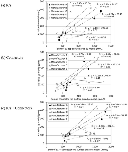
shows that there was a positive correlation between the sum of the top surface areas of ICs and connectors and their Au values: the higher the sum of the area, the higher the Au value was. The correlation with the IC top surface area was exceptionally high, with a contribution ratio (R2) of 0.97 and 0.94 for manufacturers A and B, respectively. The ratio was approximately 0.6 for manufacturers C and D. Although the data of IC top surface area for manufacturer E belonged to a narrow range and no correlation could be observed, the correlation of the top surface area of the connector was high. The contribution rate of manufacturer B was 0.96, followed by manufacturers A, C, and D (~0.85–0.90). Notably, all the manufacturers, except E, displayed evident positive correlations. With regard to the correlation with the IC + connector top surface area, although the contribution rate was marginally lower in the case of manufacturer C (0.67), manufacturers A, B, and D showed strong positive correlations (≥ 0.94). The case of manufacturer E indicates a negative correlation.
From the above results, manufacturers A, B, and D had the highest contribution rates. Thus, in these cases, it was considered that the total resource value of waste digital-camera boards could be estimated with high accuracy by measuring the sum of the top surface areas of both ICs and connectors. For manufacturer C, the estimation accuracy was higher when the top surface area of only the connector was used as an index.
IC and connector detection algorithm
We developed an algorithm that automatically detects ICs and connectors with lengths ≥2 mm from a 2D image of a board. The algorithm detects the target devices at high speed and with high accuracy by performing image processing based on the external characteristics of the device (e.g., color information, shape, and size).
Extraction of characteristic colors based on color components
An investigation of the printed circuit boards of the 26 waste digital-cameras revealed that the ICs (excluding the terminal parts) were black and rectangular (aspect ratio 1.0–3.5). Their long sides had lengths of 2–30 mm. Other features included printed letters, marks, and stickers. Unlike for the ICs, there were many cases in which a connector had two colors (e.g., white and brown or black and brown). Their shapes were nearly rectangular, and many had large aspect ratios (1.5–10.0). The long sides had lengths of 2.5–25 mm. To distinguish these ICs and connectors from other devices and the base board, we first leveraged the color information. Thus, we extracted features based on color components. The HSL method (Ohta Citation2009) was used as the color model. The hue is given as a pixel value in the order of red, orange, yellow, green, blue, purple, and red in the range of 0–255. Saturation is a measure of vividness on a scale of 0–255: zero is an achromatic gray, and 255 is a pure color. Luminance also has a scale of 0–255: zero is black, the midpoint (128) is a pure color, and 255 is white.
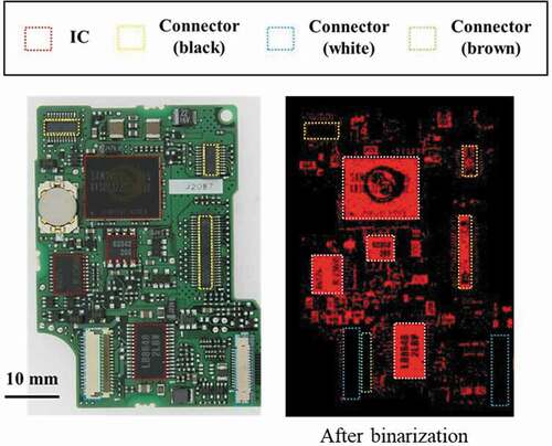
shows an example of the HSL component distribution of ICs and connectors with a board image captured under a white fluorescent lamp (Hf-type). The characteristic color of the ICs was black. However, hue had a wide range of values (40–180). Meanwhile, the saturation and luminance values were in the ranges 0–40 and 40–65, respectively. The black part of the connector was similar to the IC and had hue, saturation, and luminance of 100–180, 0–45, and 45–80, respectively. Meanwhile, its white part had values of 25–40, 15–25, and 195–205, respectively, and the brown part had values of 5–40, 10–60, and 75–110, respectively. To extract the IC from the board’s image using the characteristic black color, binarization was conducted by setting the ranges of hue, saturation, and luminance as 40–180, 0–40, and 40–65, respectively. Binarization is a type of simple image processing wherein only pixels with HSL components within these ranges are displayed in a predetermined color, and pixels outside the ranges are hidden. shows an example of these results. Parts of the ICs and connectors (black) of interest and small black devices (e.g., ceramic capacitors and transistors) with lengths ≤ 2 mm were extracted. The white and brown parts of the connectors and the green board surface were not displayed. To extract the white, black, and brown characteristic colors of the connector, it was sufficient to set an appropriate range for each HSL component and then perform binarization. A connector that has two characteristic colors is counted as two connectors. To prevent this, detected center-positions (of connectors) separated by a distance less than a certain value were regarded as belonging to one device. Only a larger area was counted in this case.
Figure 3. Example of color-component distribution based on HSL color model of IC and connector.
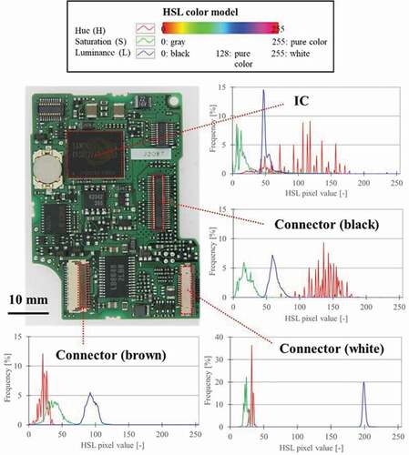
Figure 4. Extraction of IC by characteristic color.
Investigation of device detection algorithm based on color extraction
We investigated the algorithm for detecting the number of ICs and connectors from an image of a board by applying various filters based on the binarized image obtained by the color extraction procedure described above.
Color binarization based on HSL components of characteristic color
First, binarization was performed based on the range of the corresponding HSL component, such that black (which was the characteristic color of the ICs) was extracted. The range determined through a comprehensive survey of the HSL distributions provided by the mounted ICs from images of multiple types of boards included the HSL distributions of most of the ICs. Differences in HSL distribution could be observed depending on the manufacturer, deterioration, filth, etc., even among devices having an identical IC. Therefore, it was necessary to set a wide HSL range to extract the maximum number of ICs.
Extraction of outlines by average filtering
Occasionally, metal terminals around the target device, patterns of wiring on the board surface, devices having a long side of several millimeters, etc., were extracted by the above-mentioned binarization. This caused the outline of the target device to become unclear. In this case, the outline was clarified by performing a process of replacement with the average pixel value of the surroundings, e.g., 7 × 7 pixels. The method enabled us to obtain the outline of the target device and eliminate non-target small terminals, noise, etc. Thus, it was necessary to adjust the size of the averaging filter according to the size of the target device. Notably, small target devices can disappear depending on the averaging range.
Output of results
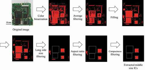
After average filtering, filling was performed to measure the particle areas and remove the fine particles. Then, based on the shape and size of the IC to be detected, filtering was performed using the preset long-side length, aspect ratio, and compactness (i.e., ratio of the extracted particle-area to the circumscribed rectangular area). Compactness filtering considers that this ratio approaches one for rectangular target devices. Because most of the ICs and connectors are rectangular, these can be extracted effectively. Finally, the number of particles, area, and position were measured by considering a particle as an IC. The basic structure of the algorithm is as follows: first, color binarization based on the HSL component distribution of the characteristic color is performed. Then, outline extraction is achieved by average filtering. Next, the holes are filled in. Subsequently, average filtering is performed for a second time. The particles are then extracted via filtering based on the long-side length, aspect ratio, and compactness. Finally, the total area of the extracted particles is measured.
shows the results of the image processing at each step when an IC is targeted. A similar algorithm structure was used for connector detection. Here, the threshold values for color binarization and filtering were varied according to those for connectors. Finally, the result of two medium-sized ICs was output by excluding large-sized square particles, elongated particles with high aspect-ratios, and particles with a low compactness (cable parts), as shown in the lower row of the figure.
Figure 5. Algorithm for IC extraction.
IC and connector detection test
Detection test conditions
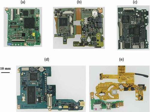
Assuming normal camera photography at a recycling plant, 46 types of boards (counted as two types if a board was dual-sided) were removed from the 26 waste digital-camera models. These were placed under a white fluorescent lamp, and 46 2D digital images were acquired. An Olympus digital camera (CAMEDIA SP-560UZ) was used for image acquisition, and automatic photography mode was used. All the images were of size 3,264 × 2,448 pixels. (a–e) shows an example of an image of a board. The size and color of the board and the type and number of mounted electronic devices varied widely depending on the board type, and no two of these were identical. In general, the board surface shown in (a) and (b) is green. However, dark green turquoise (such as (c) and (d)) and flexible boards (e) were also observed.
Figure 6. Examples of images of waste digital-camera board. (a) (b) Green boards, (c) dark-green board, (d) blue-green board, (e) flexible board.
The algorithm discussed in Section 3.2 was applied to the board images, and IC and connector detection tests were performed. After reading the image files and performing a series of image processing based on the algorithm, a new program that displays the measurement results of the area and position of extracted devices on a screen was developed using LabVIEW (system-development software) and Vision (image analysis software), both of which are from National Instruments. The program enabled the continuous processing of multiple image files contained in a folder. lists the ranges used for color binarization and the various types of filtering. With regard to the connectors (white), there were cases in which the HSL component distribution was different even for white. Therefore, these two types were used. Although the number of components was small, a few were detected in the ranges of both IC and connector (black). These were compared with the actual device and determined to be ICs.
Table 2. Ranges for color binarization and filtering
IC detection results
shows the IC detection results for 46 board images. There were four types of IC depending on the long-side dimensions: 2–5, 5–10, 10–15, and ≥ 15 mm. In the table, the third, seventh, and rightmost columns present the sum of the measured top surface areas, sum of all areas including those of the devices that were erroneously identified as ICs, and ratio of the two, respectively.
Table 3. Results of IC/connector detection tests for 46 types of waste digital-camera boards
Of the 240 ICs mounted on the 46 boards, 133 (55%), 69 (29%), 34 (14%), and 4 (1.7%) had long sides of 2–5, 5–10, 10–15, and ≥ 15 mm, respectively. The sum of the top surface areas of the ICs with long sides of 2–5 mm was 1,006 mm2 (12%). That is, although these ICs accounted for over 50% of the total number of ICs, the sum of their areas was approximately 10% of the total. Considering that the amount of Au contained in an IC depends on the area of the top surface, most of the resource value of the board could probably be calculated by detecting ICs with long sides ≥ 5 mm with high accuracy.
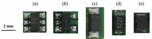
Of the 240 mounted devices, only 176 were detected correctly. Thus, the IC detection rate was 73%, which is considered insufficient. The number of false detections of non-IC devices as ICs was 212, accounting for 55% of the total number of detections. This was caused by the exceptionally high false detection rate when the long side was 2–5 mm (186, 68%). Many types of devices have similar colors and shapes in this long side-length category, and most cases included false detections of transistors, diodes, black tantalum capacitors, etc. ( (a–e)). The total number of ICs that could not be detected was 64. Of these, 47 (73%) had a long side of 2–5 mm. In many cases, the ICs were extracted in a state of being integrated with adjacent ICs or similar devices in the extraction process, and were then removed by filtering the long-side length or compactness.
Figure 7. Example of devices similar to ICs. (a) IC, (b) transistor, (c) diode, (d) tantalum capacitor (black), (e) inductor.
In contrast, the sum of the detected top surface areas was 8,566 mm2. This is 105% of the actual sum of areas, i.e., it is significantly close. This is partly because there was an error in the detected area of each IC, and the areas of false detections and non-detections compensated each other to a certain extent. However, the main cause was probably related to ICs with long sides of 2–5 mm, which had negligible impact on the sum of areas. The IC detection rates were high at 83%, 85%, and 100% for long-side lengths of 5–10, 10–15, and ≥ 15 mm, respectively. For the sum of areas, the canceling effect between false detection and non-detection yielded remarkable estimation accuracies (93%, 102%, and 98%, respectively). The IC detection rate improved because although the transistors and inductors inside similar devices were relatively large, as shown in , almost no diode or tantalum capacitor (black) with long sides ≥ 5 mm were mounted. This tendency was more pronounced for long-side lengths ≥ 10 mm.
From the given information, the applicable range of this algorithm includes long sides ≥ 5 mm, accounting for approximately 90% of the resource value of all ICs. Moreover, such devices could be detected with relatively good accuracy. However, problems remain with respect to misidentification and non-detection. Therefore, the algorithm needs to be improved to realize highly accurate detection. This is discussed in the next section.
Connector detection results
also shows the connector detection results for the 46 board images. The connectors with long sides ≥ 2.5 mm were classified into three types according to their characteristic colors: white, black, and brown. Of the 115 connectors mounted, 59 (51%), 39 (34%), and 17 (15%) had white, black, and brown colors, respectively. The proposed algorithm correctly detected 99 (86%) of the 115 connectors, demonstrating its effectiveness. In contrast, of the total number of cases (136), false detections occurred in 37 (27%). Furthermore, there was a tendency toward a large number of false detections for a small number of missed detections. Therefore, the algorithm can be improved further. The total area detected was 4,114 mm2, which is marginally less than the total mounted-connector surface area of 4,339 mm2 (95%). This is because the average filtering performed twice in this algorithm removed small terminals around the connector and partially removed its outline.
Considering each feature color, the detection accuracy was highest for the white connectors (57 out of 59 mounted white connectors were detected correctly), followed by the brown connectors. There were five cases of misdetections wherein the flexible board part that connected the boards was brown and identified erroneously. Both estimations of the sum of top surface areas were less than the actual values owing to the abovementioned effects. In contrast, the black connectors, which accounted for less than 30% of the number of mounted devices, were relatively difficult to detect. The detection rate for these was less than 70% (67%), with a higher number of false detections (17). Examples of falsely detected components include crystal oscillators, cable connection parts, and circuits with black colors on their board surfaces. False detections also occurred in cases of variations in shades of black (depending on the individual connectors), wherein the range of HSL components did not match.
Result of IC and connector detection
shows the sum of the top surface area per board and the standard deviation for the IC and connector detection results. The total area of the detected devices was 12,680 mm2, whereas the sum of the top surface areas of the mounted devices was 12,529 mm2. The results were within the range of the data. Considering only this value, it can be stated that accurate estimations are feasible (101%). However, the estimation for ICs was 105% and that for connectors was 95%. Thus, the errors between the two were offset. We verified that the estimations of the sum of the areas, the area per board, and its standard deviation are close to the data of all the mounted devices. As described in Sections 4.2 and 4.3, problems with IC and connector detection need to be solved. However, the present algorithm is effective for estimating the resource value of printed circuit boards mounted on waste digital-cameras of leading manufacturers. It should also be noted that the authors have verified that the types and numbers of devices mounted on printed circuit boards of mobile phones and smartphones do not differ significantly from those for digital cameras. Therefore, it can be assumed that the proposed algorithm can be applied conveniently to these small-sized waste home appliances.
Table 4. Results of IC + connector detection tests for 46 types of waste digital-camera boards
Consideration of main causes of false/non-detection and countermeasures
As demonstrated previously, the sum of the top surface areas of the ICs and connectors can be detected correctly using the detection algorithm via 2D images, and the total resource value of the board can be estimated with high accuracy. However, particularly for ICs with long sides of 2–5 mm, the detected area is marginal, and there are many cases of false and non-detections. In our experiments, it was difficult to correctly detect black connectors without omissions. Considering that a wider variety of waste printed circuit boards would be the target of the algorithm in the future, it is highly important to analyze the factors of false detection and non-detection and investigate measures to improve the accuracy of the algorithm.
Four factors were identified as the main causes of false detection and non-detection: (1) presence of non-target devices with similar appearance characteristics, (2) variations in color components between devices of a similar type, (3) adjacency of similar devices, and (4) appearance of unforeseen colors. Cause (1) indicates that there were other devices with characteristic color of components, long sides, aspect ratios, and compactness similar to those of ICs and connectors. A prominent example is the misidentification of transistors, diodes, tantalum capacitors (black), and inductors with long-sides of 2–5 mm (see (a–e)). It was exceptionally difficult to identify these devices using only the proposed algorithm because of the negligible difference in their external characteristics (except for terminals). In addition, there were many cases of false detections with a combination of connectors (black), crystal oscillators, and black circuits on the board surface. In certain cases, a crystal oscillator with an Al cover was incorrectly identified as a connector (white). In these examples related to Cause (2), it was necessary to set a range such that more similar colors could be included while conducting binarization based on the distribution of HSL components. Thus, the mixing of non-target devices with similar colors could increase. In addition, when the board-surface color – which occupied a large proportion of the area – contained similar colors, it was particularly difficult to extract devices based on differences in their HSL components. In one example, because the board surface was nearly black, an outline of the IC could not be extracted by average filtering, and surrounding particles were integrated in the hole-filling process. In the future, as a measure for reducing the number of false detections and non-detections, it may be feasible to scrutinize the appearance characteristics of the main non-target devices and detect these using characteristics different from those of the target device, thereby removing them in advance. For example, ICs with long sides of 2–5 mm generally have six terminals on their long side. However, transistors have five, and diodes have two on their short sides ( (a–e)). This enables identification by counting the number of solder points around the detected device (solder is extracted conveniently by feature color). Furthermore, as shown in (d), alphanumeric characters are highly likely to be printed on the top surfaces of tantalum capacitors (black), and these should have gray strips on the edges. Alternatively, it may be feasible to use three-dimensional (3D) information. If information in the height direction can be obtained with high accuracy, it would be convenient to remove the board surface or conduct identification based on differences in device heights. The method of designing image processing based on feature information obtained in advance and performing sequential processing is called “rule-based image processing.” It requires a precise set of rules (e.g., filtering ranges). The deterioration of a wide variety of types, sizes, and shapes of devices with time and because of wear (which is generally the case for small waste household appliances) places a limitation on the design of rules that would apply to all these. To overcome this issue, an approach wherein a machine-learning algorithm learns the acquired appearance-feature information and conducts identification automatically would be effective. For example, template matching (a type of pattern recognition) that uses images of ICs and other devices including solder parts, or device-image training for deep learning should be considered. For these approaches, the designer would not be required to provide rules in advance. Furthermore, components with characteristics similar to those of the target component (previously used as training data) would be detected through adequate learning. Therefore, it would be feasible to mitigate the effects of device deterioration, surface contamination, and damage to a certain extent. The above considerations are summarized in (1).
Table 5. Main causes of false/non-detection and countermeasures
With regard to Cause (2), the range of saturation (S) and luminance (L) may differ owing to device deterioration and differences in manufacturer. Therefore, it is necessary to set a range that includes more similar colors (see Section 3.2). In contrast, as described, the likelihood of mixing non-target devices with similar colors and the number of misidentified transistors, diodes, tantalum capacitors (black), and inductors increase. In these cases, the detection accuracy can be increased by segmenting the range finely according to the differences in the HSL component distribution, This is feasible even for an identical type of device. Furthermore, as described in Section 4.1, we set two patterns of color binarization range for the connector (white), and we could detect connectors with marginally different shades with nearly no omissions. This was so even in the same white connector class. Although an increase in the pattern settings of the HSL component tends to increase the detection time, the proposed algorithm consists of relatively simple image processes. Furthermore, high-speed processing is feasible. Thus, each board image can still be processed within 1 s. These considerations are presented in (2).
With regard to Cause (3), there were many cases of ICs mounted in parallel. If devices are arranged at small intervals, these are likely to be integrated during binarization owing to the influence of shadows, etc. This results in the formation of large particles. Because there is no step in which particles can be divided during subsequent processing, these are removed by long-side size filtering. Therefore, these are not detected. This, along with Cause (4), were the main causes of non-detection of relatively large ICs with long sides ≥ 5 mm in our experiments. Although it is difficult to prevent adverse effects while using the proposed algorithm to address this phenomenon, it may be feasible to develop a countermeasure. We could detect devices in parallel by constructing a machine-learning algorithm that uses device images as training data, as described for Cause (1). In addition, if information in the height direction can be obtained, it would contribute to the extraction of the outline of each device. These considerations are shown in for Cause (3).
Cause (4) is a phenomenon related mainly to the use of stickers (mostly white) attached to the IC and dirt on the board or device surface. In certain cases, a barcode sticker that indicates the board type is attached. If the sticker area on the IC is large, the IC part becomes a particle with large holes after binarization, which cannot be filled by the hole-filling process. Compactness is reduced considerably, and the IC is removed. This was the main reason for the non-detection of relatively large ICs in our experiments. In addition, the presence of dirt results in an HSL component distribution that differs from the characteristic color. This frequently affects image processing adversely. With regard to stickers, it is necessary to examine the appearance characteristics and consider the introduction of an algorithm to remove these in advance. This has been indicated as a measure to mitigate Cause (1). The introduction of machine learning algorithms would be highly effective. We plan to study this issue in the future. These considerations are listed in .
Conclusion
Herein, an algorithm was constructed to straightforwardly and rapidly evaluate the resource values of printed circuit boards in small waste home appliances. It automatically measures the sum of the top surface areas of ICs/memory and connectors, which account for over 80% of the resource value of mounted devices. A program that performs image processing on multiple 2D digital circuit board images was developed based on a simple algorithmic structure. First, color binarization based on the HSL component distribution of the characteristic color was performed. This was followed by outline extraction using average filtering, then hole filling. Subsequently, average filtering was repeated. The particles were extracted by filtering based on the long-side length, aspect ratio, and compactness. Finally, the total area of the extracted particles was measured.
According to the results of detection tests performed using the constructed algorithm on 46 types of boards removed from 26 models of waste digital-cameras, 1) the detection rate of ICs with sides ≥ 2 mm was 73%, and 2) the ratio of the estimated value of the total top surface to its measured value was approximately 105%. The main reason for the low detection rate is that ICs with long sides of 2–5 mm were frequently identified erroneously as similar devices, such as a transistor or diode. In contrast, for long sides ≥ 5 mm, the ratio of the total area was approximately 90%. In addition, falsely detected areas and undetectable regions were offset to a certain extent. Thus, the estimated value of the total area was highly accurate. The connector detection rate was 86%. However, high detection accuracies of 94% and 97% were achieved for cases of white and brown colors, respectively, which accounted for over 70% of the number mounted. However, the detection accuracy of the black connectors was relatively low. The ratio of the estimated sum of areas to the actual value was 95%, which is highly accurate. The accuracy of estimating the sum of the top surface areas of both ICs and connectors was 101%. We clarified that the total resource value of a board could be estimated nearly correctly for each manufacturer by using this factor as an index. Because the structure of the constructed algorithm is simple and can be applied to multiple target devices, high-speed processing can be achieved when implementing automatic detection. Since this time the authors targeted only waste digital-camera boards, they plan to expand the scope to include smartphones, mobile phones, video cameras, etc., which have high resource value as well as digital-cameras, as the next step. As for electronic devices to be detected, not only ICs and connectors, but also transistors, diodes, ports, etc. with high Au content will be included.
An analysis revealed the following factors to be causes of false detection and non-detection of ICs and connectors: the presence of non-target devices with similar appearance characteristics, spread of color components among similar devices, arrangement of similar devices adjacently, and appearance of unforeseen colors (a significant factor that causes non-identification). The following countermeasures are proposed to address these problems: the use of machine-learning algorithms, pre-removal of similar devices and adhesive stickers, use of 3D information, and precise range segmentation of color components.
Data availability
The authors confirm that the data supporting the findings of this study are available within the article.
Acknowledgment
This study is based on results obtained in a project (code: P17001) commissioned by the New Energy and Industrial Technology Development Organization (NEDO).
Disclosure statement
No potential conflict of interest was reported by the author(s).
Additional information
Funding
Notes on contributors
Naohito Hayashi
Naohito Hayashi is a leader of Resource Value Creations Research Group, Environmental Management Research Institute, National Institute of Advanced Industrial Science and Technology (AIST).
Shigeki Koyanaka
Shigeki Koyanaka is a chief senior researcher of Resource Value Creations Research Group, Environmental Management Research Institute, AIST.
Tatsuya Oki
Tatsuya Oki is a deputy director of Environmental Management Research Institute, AIST.
References
- Adibhatla, V. A., H. C. Chih, C. C. Hsu, J. Cheng, M. F. Abbod, and J. S. Shieh. 2020. Defect detection in printed circuit boards using you-only-look-once convolutional neural networks. Electron 9:1547. doi:https://doi.org/10.3390/electronics9091547.
- Adibhatla, V. A., H. C. Chih, C. C. Hsu, J. Cheng, M. F. Abbod, and J. S. Shieh. 2021. Applying deep learning to defect detection in printed circuit boards via a newest model of you-only-look-once. Math. Biosci. Eng. 18:4411–28. doi:https://doi.org/10.3934/mbe.2021223.
- Aizawa, H., Y. Hirai, and S. Sakai. 2009. Recycling of small electrical and electronic equipment waste. J. Mater. Cycles Waste Mgt. 20:371–82. (in Japanese).
- Chiah, C. K., C. X. Teng, C. K. Siew, and S. Y. Chark. 2012. 2-d location pointing system for individual component on device under test by using LabVIEW. Proc. 2012 IEEE Conf. Sustain. Util. Dev. Engin. Tech., Kuala Lumpur, Malaysia, 248–52.
- Dai, W. T., A. Mujeeb, M. Erdt, and A. Sourin. 2020. Soldering defect detection in automatic optical inspection. Adv. Eng. Inform. 43:101004. doi:https://doi.org/10.1016/j.aei.2019.101004.
- Dervisevic, I., D. Minic, Z. Kamberovic, V. Cosovic, and M. Ristic. 2013. Characterization of PCBs from computers and mobile phones, and the proposal of newly developed materials for substitution of gold, lead and arsenic. Environ. Sci. Pollut. Res. 20:4278–92. doi:https://doi.org/10.1007/s11356-012-1448-1.
- Esaki, H., K. Kagii, T. Umezaki, and T. Horikoshi. 2006. Hierarchical automatic classification system of electronic parts. Trans. Inst. Elect. Engin. Japan. C 126:1447–53. (in Japanese).
- Hayashi, N., S. Koyanaka, and T. Oki. 2019. Constructing an automatic object-recognition algorithm using labeling information for efficient recycling of WEEE. Waste Manag. 88:337–46. doi:https://doi.org/10.1016/j.wasman.2019.03.065.
- Hu, B., and J. H. Wang. 2020. Detection of PCB surface defects with improved Faster-RCNN and feature pyramid network. IEEE Access 8:108335–45. doi:https://doi.org/10.1109/ACCESS.2020.3001349.
- Lefkaditis, D., and G. Tsirigotis. 2010. Intelligent optical classification system for electronic components. Electron. Electr. Eng. 98:10–14.
- Li, Y. T., P. Kuo, and J. I. Guo. 2021. Automatic industry PCB board DIP process defect detection system based on deep ensemble self-adaption method. IEEE Trans. Compon. Packaging Manuf. Technol. 11:312–23. doi:https://doi.org/10.1109/TCPMT.2020.3047089.
- Li, J., W. Y. Li, Y. Q. Chen, and J. A. Gu. 2021. A PCB electronic components detection network design based on effective receptive field size and anchor size matching. Comput. Intell. Neurosci. 6682710. doi:https://doi.org/10.1155/2021/6682710.
- Lian, J., L. T. Wang, T. Y. Liu, X. Ding, and Z. G. Yu. 2021. Automatic visual inspection for printed circuit board via novel Mask R-CNN in smart city applications. Sustain. Energy Technol. Assess. 44:101032.
- Matsunaga, E., T. Minowa, K. Takahashi, H. Arai, and T. Sawada. 2015. Resource visualization technology for metal contents of printed circuit boards –Various electronic component detection using image processing. Proc. 26th Ann. Conf. Japan Soc. Mater. Cycles Waste Mgmt., Fukuoka, Japan, 169–70. (in Japanese).
- MineralPrices.com. 2020. Metal prices April 2020 in review. Accessed June 28, 2020. https://mailchi.mp/3a204a7c02c4/mineralpricescom-april-2020-4805568
- Mogi, T., M. Namekawa, and Y. Ueda. 2012. Detection of insertion error parts in electronic boards using HSV color format. Proc. 12th I.C. Intell. Sys. Design Apps., Kochi, India, 357–62.
- Muto, S. 1995. Mathematical statistics, 54–57. Tokyo, Japan: Asakura Publishing Co. Ltd. (in Japanese).
- Nishimura, K., M. Yanabe, M. Hashimoto, T. Araki, T. Nagatani, T. Moriyama, and S. Maeda. 2018. Proposal of electronic component visual inspection method with histogram-based local feature. J. Jpn. Soc. Precis. Eng. 84:664–70. (in Japanese). doi:https://doi.org/10.2493/jjspe.84.664.
- Nishimura, K., M. Yanabe, T. Nagatani, T. Moriyama, and S. Maeda. 2019. Proposal on improvement of defect identification performance by dimensional reduction focusing on localization of HOG feature in electronic component inspection. J. Jpn. Soc. Precis. Eng. 85:469–76. (in Japanese). doi:https://doi.org/10.2493/jjspe.85.469.
- Ohta, N. 2009. Color engineering, 45–62. Tokyo, Japan: Tokyo Denki University Press. (in Japanese).
- Oki, T. 2014. Physical separation technology to support the strategic development of urban mining –development of unused/hard-to-use resources and a future vision of resources for Japan. Synthes. Engl. Ed. 6:232–40.
- Silva, L. H. D., A. A. F. Junior, G. O. A. Azevedo, S. C. Oliveira, and B. J. T. Fernandes. 2021. Estimating recycling return of integrated circuits using computer vision on printed circuit boards. Appl. Sci. -Basel 11:2808. doi:https://doi.org/10.3390/app11062808.
- Xia, S. Y., F. Wang, F. Xie, L. Huang, Q. Wang, and X. Ling. 2021. An efficient and robust target detection algorithm for identifying minor defects of printed circuit board based on PHFE and FL-RFCN. Front. Phys. 9:661091. doi:https://doi.org/10.3389/fphy.2021.661091.
- Ye, R. F., C. S. Pan, P. Y. Hung, M. Chang, and K. Y. Chen. 2020. Detection and classification of printed circuit board assembly defects based on deep learning. Chi. J. Mech. Eng. 41:401–07.