
 ?Mathematical formulae have been encoded as MathML and are displayed in this HTML version using MathJax in order to improve their display. Uncheck the box to turn MathJax off. This feature requires Javascript. Click on a formula to zoom.
Abstract
A method to model the metastable phase formation in the Cu–W system based on the critical surface diffusion distance has been developed. The driver for the formation of a second phase is the critical diffusion distance which is dependent on the solubility of W in Cu and on the solubility of Cu in W. Based on comparative theoretical and experimental data, we can describe the relationship between the solubilities and the critical diffusion distances in order to model the metastable phase formation. Metastable phase formation diagrams for Cu–W and Cu–V thin films are predicted and validated by combinatorial magnetron sputtering experiments. The correlative experimental and theoretical research strategy adopted here enables us to efficiently describe the relationship between the solubilities and the critical diffusion distances in order to model the metastable phase formation during magnetron sputtering.
Classification:
1. Introduction
During energetic vapor phase condensation, for example by magnetron sputtering and cathodic arc deposition, the formation of metastable phases is often observed. Generally, this is attributed to kinetically limited growth processes that govern thin film structure evolution.[Citation1–3] For thin films deposited at low temperatures, surface diffusion is the underlying physical mechanism that controls metastable phase formation.[Citation1–3] The atomic mobility can be studied using the temporal dependence of the surface diffusion distance of an atom as given by Einstein [Citation4]:(1)
(1)
where X is the diffusion distance, Ds is surface diffusivity and t is the time. Based on Equation (1), Cantor and Cahn [Citation5] proposed the following equation to describe the deposition rate and temperature dependence of the diffusion distance during thin film deposition:(2)
(2)
where ν is the vibrational frequency of surface atoms (~1013 s−1 [Citation6]), a is the individual jump distance, rD is the deposition rate, Qs is the activation energy for surface diffusion, k is the Boltzmann constant and T is the substrate temperature during deposition. Saunders and Miodownik [Citation7] also considered the effect of bulk diffusion and modified Equation (2) accordingly in order to investigate the metastable phase formation of Cu0.57Ag0.43, Pd0.58Rh0.42, Cu0.885Sn0.115 and Cu0.895Sn0.105 thin films. The surface diffusion distances were calculated as a function of temperature.[Citation7] Guided by the experimental phase formation data, the critical surface diffusion distances were estimated around an experimentally determined phase boundary.[Citation7] Therefore, Saunders and Miodownik [Citation7] have described the metastable phase formation for thin films at experimentally determined phase boundaries. However, no modeling attempt has been undertaken to predict metastable phase formation diagrams covering the whole composition range.
Metastable phase formation diagrams can be compiled based on experimental phase formation data of individual deposition experiments [Citation8] or from combinatorial thin film synthesis experiments.[Citation9–11] The CALPHAD (Computer Coupling of Phase Diagrams and Thermochemistry) approach provides thermodynamic input to study metastable phase formation [Citation7] and has been applied to describe the metastable solubility limit in a system during thin film deposition, based on Gibbs energy versus composition (G vs. x) diagrams.[Citation7,13–15] Using ab initio calculations, the metastable solubility limit and formation energy versus composition (Ef vs. x) can be estimated.[Citation16–18] Together with experimental phase formation data, ab initio data has recently been employed to estimate the activation energy for surface diffusion during metastable phase formation.[Citation19] It was demonstrated for sputtered Cu–W thin films that the activation energy data obtained [Citation19] can be utilized to calculate the surface diffusion distance using Equation (2). Recently, attention has been given to immiscible Cu–W and Cu–V systems (for which phase diagrams are shown in Figure ). The Cu–W thin films investigated by Vüllers and Spolenak [Citation20] show a desirable property combination: W’s high hardness and thermo-mechanical stability and Cu’s excellent thermal conductivity and electrical performance, thereby allowing for possible applications including thermal management, high power and high voltage appliances. The Cu–V thin films feature excellent thermal stability, and have been applied as seed layers for Cu interconnects.[Citation21–23]
Figure 1. Stable Cu–W (a) and Cu–V [Citation36] (b) phase diagrams calculated using the CALPHAD approach. The Gibbs energy expressions of all the phases are provided in Appendix A.
![Figure 1. Stable Cu–W (a) and Cu–V [Citation36] (b) phase diagrams calculated using the CALPHAD approach. The Gibbs energy expressions of all the phases are provided in Appendix A.](/cms/asset/fd20511e-5571-415f-a2c7-5a8e4b665827/tsta_a_1167572_f0001_oc.gif)
The aims of the present work are (1) to develop a model with which to describe the relationship between solubilities and critical diffusion distances based on experimental phase formation data,[Citation19] (2) to predict metastable Cu–W and Cu–V phase formation diagrams and (3) to validate these predictions using additional thin film growth and characterization experiments.
2. Experimental and theoretical methods
Cu–V thin films were synthesized by DC magnetron sputtering in an industrial CemeCon 800/9 system (CemeCon AG, Würselen, Germany), where the combinatorial approach [Citation9–12] with split Cu and V targets was applied. The base pressure was less than 10−4 Pa and the argon partial pressure was 0.35 Pa during deposition. The distance between target and substrate was 9.5 cm. Si (100) and Al2O3 (0001) wafers were used as substrates. One set of thin films was deposited at a power density of 0.91 W·cm−2 and temperature of 240 °C, respectively. The power density is equal to the power applied to the target, divided by the target size (50 × 8.8 cm2). The substrate temperature was measured using three thermocouples clamped to the substrate surface. More information about deposition setup can be found elsewhere.[Citation19] Composition of the samples was analyzed with a scanning electron microscope (SEM; JEOL JSM 6480, JEOL Ltd., Tokyo, Japan) equipped with an EDAX2000 energy dispersive X-ray spectrometer (EDX, EDAX Inc., Mahwah, NJ, USA). The thin film thickness was measured by cross-sectional SEM and the deposition rate was calculated by dividing film thickness by deposition time. Structural analysis was carried out by means of X-ray diffraction (XRD) with a Bruker AXS D8 Discover General Area Diffraction Detector System (GADDS, Bruker AXS GmbH, Karlsruhe, Germany). The strain-free lattice parameters were determined using the sin2ψ method.[Citation24,25] These experimental data were then applied as the input in predicting metastable phase formation diagrams for the Cu–V system. Additional combinatorial sputtering processes were carried out at different power densities (0.91, 3.64 and 7.28 W·cm−2) and different substrate temperatures (80–340 °C). This phase formation data was used to validate the predictions.
Lattice parameters and formation energetics of body centered cubic (bcc) and face centered cubic (fcc) Cu–V solid solutions were investigated using ab initio calculations utilizing the coherent potential approximation (CPA) and special quasi random structure (SQS) approaches. For CPA, the exact muffin tin orbitals (EMTO) formalism [Citation26,27] based on Green’s function [Citation28] and full charge density [Citation29] techniques was used. The generalized gradient approximation (GGA) [Citation30] was applied. The core states were fixed and the total energy was converged within 10−7 Ry. For SQS, 16 atoms per unit cell of CuxW1-x (x = 0.0625, 0.125, 0.1875, 0.25, 0.5, 0.75, 0.8125, 0.875 and 0.9375) for both bcc and fcc phases were used for calculations in the Vienna ab initio simulation package (VASP).[Citation31] The valence electrons were explicitly treated by projector augmented plane-wave (PAW) potentials.[Citation32] The GGA method was performed using Blöchl corrections for the total energy [Citation33] with a plane-wave cutoff energy of 500 eV and a convergence criterion for the total energy of 0.01 meV. Integration in the Brillouin zone was done on appropriate k-points, which was determined after Monkhorst-Pack.[Citation34] Migrations of Cu and V atoms in bcc (110) and fcc (111) surfaces were calculated using ab initio calculations in order to obtain surface diffusion activation barriers. A detailed description of the method can be found elsewhere.[Citation19]
The CALPHAD approach was utilized to calculate stable phase diagrams of the Cu–W and Cu–V systems considering the phase equilibria and thermodynamic data from [Citation35] and [Citation36], respectively. FactSage software [Citation37] was utilized for the calculations. Gibbs energy expressions for all of the phases are provided in Appendix A. While differing from [Citation35], generally accepted Gibbs energy functions for pure Cu and W [Citation38] were used in the present calculation. Therefore, the temperature of the invariant reaction (Liquid#2 = bcc + Liquid#1) in the Cu–W phase diagram is 3270 °C, compared to 3240 °C in [Citation35]. As no experimental information is available for this reaction, the calculations in this work, as well as in [Citation35], should therefore be regarded as hypothetical. Moreover, the Gibbs energies for the Cu–V system are identical to those employed in [Citation36].
3. Results and discussion
3.1. A model to describe the relationship between solubilities and critical diffusion distance
Experimental phase formation data in the Cu–W thin films were obtained,[Citation19] as shown in Figure (a). The maximum solid solubility limit of Cu in bcc-W is found to be approx. 78 at.%. It was suggested that as X reaches a critical diffusion distance (Xc), the formation of the second phase and hence decomposition is observed experimentally.[Citation19] Equation (2) can thus be rewritten including Xc:(3)
(3)
Figure 2. Metastable phase formation in Cu–W thin films: (a) experimental data of thin films grown at different power densities [Citation19]; (b) structure evolution for CuxW1-x thin films at a certain deposition rate (Tc: critical temperature; Xc: critical surface diffusion distance); and (c) composition dependence of Xc at the bcc and fcc surfaces.
![Figure 2. Metastable phase formation in Cu–W thin films: (a) experimental data of thin films grown at different power densities [Citation19]; (b) structure evolution for CuxW1-x thin films at a certain deposition rate (Tc: critical temperature; Xc: critical surface diffusion distance); and (c) composition dependence of Xc at the bcc and fcc surfaces.](/cms/asset/986789dd-f5e9-410a-b4e9-d5c3b5177dc8/tsta_a_1167572_f0002_oc.gif)
where Tc denotes the critical temperature for each CuxW1-x composition at a certain deposition rate (rDn). The phase formation data (Figure (a)) are subsequently summarized in Figure (b). If the substrate temperature is less than Tc, the diffusion distance of atoms on bcc or fcc surfaces is smaller than Xc, meaning that the formation of thermodynamically stable phases is prevented by kinetic limitations in that the atomic mobility is insufficient. If the temperature increases to a value equal to or larger than Tc, atomic mobility is enhanced, causing decomposition of the metastable solid solutions into bcc + fcc phases. Thus, being able to quantify the critical diffusion distance is essential for modeling metastable phase formation diagrams. Using Equation (3), the composition dependence of Xc was obtained, as is shown in Figure (c). Activation energies (Qs) derived from experimental data [Citation19] were used in the calculations. It is interesting to note that all experiments result in a unified Xc vs composition behavior, suggesting that Xc is in fact a temperature-independent and deposition rate-independent property.
In order to model metastable phase formation (Figure (a)), it is essential to determine the composition dependence of Xc. In other words, if Xc for each x in CuxW1-x is known, one can obtain the corresponding Tc using Equation (3) and the whole metastable phase formation diagram can be calculated. The mutual stable solid solubility at the growth temperature between Cu and W is negligible [Citation35], as shown in the calculated Cu–W phase diagram (Figure (a)). However, metastable solid solubility (z) of Cu in bcc-W and W in fcc-Cu is obtained in magnetron sputtering experiments [Citation19]. z is the composition of the boundary between single-phase and two-phase regions. The maximum metastable solubilities (zmax) for Cu in bcc-W and W in fcc-Cu at 110 °C and the power density of 0.92 W·cm−2 are about 78.0 at.% Cu and 22.0 at.% W [Citation19], respectively. To compile a metastable phase formation model, the relationship of Xc and z needs to be determined, based on experimental data. The Xc vs. x diagram (Figure (c)) has been transformed into two diagrams (Figure (a) and (b)) describing Xc vs. z for the bcc and fcc phases, respectively. Each dataset shows a similar trend. Independent of crystal structure, the relationship of Xc and z can be fitted well using the following sigmoid function:(4a)
(4a)
(4b)
(4b)
Figure 3. Xc vs. z plot: experimental data and fitted curves using Equation (Equation5(5)
(5) ) for both bcc (a) and fcc (b) phases in the Cu–W system.
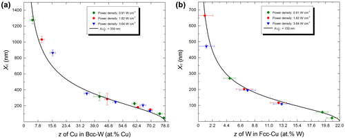
where zmax denotes maximum metastable solid solubility and zmin denotes the stable solid solubility from the equilibrium phase diagrams (Figure (a) and (b)). A is the critical diffusion distance at half metastable solid solubility (when ) and will be denoted as
. In the Cu–W system, zmin ≈ 0 for both bcc and fcc phases (see Figure (a)). According to experimental data [Citation19], zmax ≈ 78 at.% Cu for bcc phase and zmax ≈ 22 at.% W for fcc phase. By fitting each dataset in Figure (a) and (b), the value of B is obtained ≈2 for both bcc and fcc phases and is henceforth assumed to be a constant. Different values of
for the fitted curves can be obtained, and are shown in Figure . Therefore, Equation (4b) can be written in the following form:
(5)
(5)
This model defines the surface diffusion required for atoms to drive second phase formation and reveals the relationship between solubilities and the critical diffusion distance. If z = zmax, meaning the phase is highly unstable, then Xc = 0, indicating that the atoms need only a minute diffusion distance in order to form a second phase. If z = zmin, then Xc = +∞, denoting that the phase is thermodynamically stable and that the system is always in its equilibrium state.
3.2. A model based research strategy for predicting metastable phase formation diagrams
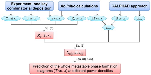
A combination of Equations (3) and (5) enables the prediction of metastable phase formation diagrams, based on a correlative experimental and theoretical research strategy. This method is delineated in the flowchart in Figure . One can calculate the diagram at a certain power density with input of the following variables: Tc1, rD, a, Qs, zmax and zmin. By varying the power density, rD is affected and the metastable phase formation diagram changes accordingly. Assuming that rD is directly proportional to power density, the diagrams at different power densities can be predicted. In Figure , Tc1 denotes one critical temperature determined by experiments. rD and a can also be acquired using experiments. Ab initio calculations can be used to obtain a, Qs and zmax, while the CALPHAD approach can be applied to describe both zmax and zmin.
Figure 4. Flowchart of the present research strategy to predict metastable phase formation diagrams for sputtered thin films.
Generally, one key combinatorial deposition together with the above-described calculations is needed to map metastable phase formation diagrams, provided the following necessary requirement is fulfilled: the experimental phase formation data has to cover the complete composition space, containing all of the phase boundaries to be modeled. For instance, one cannot obtain a critical temperature for the fcc phase based only on experimental data at 350 °C, because all of the data on the Cu-rich side exhibits bcc + fcc two phase structures (see Figure (a)).
3.3. Modeling of the Cu–W system
The phase formation data obtained from one deposition performed at a temperature of 250 °C and power density of 0.91 W·cm−2 have been selected to model the Cu–W system. XRD profiles of the Cu–W thin films are shown in Figure (a), where 2θ positions of pure Cu [Citation39] and W [Citation40] are added as references. Thin films with Cu concentrations below 59.8 at.% are composed of a bcc solid solution, while those with Cu concentrations above 96.0 at.% are composed of an fcc solid solution. The thin films with Cu concentration ranging from 61.4 to 94.2 at.% contain bcc and fcc phases. Therefore, Tc1 is equal to 250 °C at the composition of ~60.6 and ~ 95.1 at.% Cu for the bcc and fcc phases, respectively. Previously,[Citation19] a, zmax and Qs have been described by ab initio calculations. zmin equaling zero was obtained here using the CALPHAD approach (Figure (a)). It is known that grain size is affected for example by the deposition rate and substrate temperature [Citation42]. The model proposed here is based on the phase formation data only. Microstructural features such as grain size information are not included at present.
Figure 5. XRD profiles of (a) Cu–W thin films deposited at a temperature of 250 °C and power density of 0.91 W·cm−2; (b) Cu–V thin films deposited at a temperature of 240 °C and power density of 0.91 W·cm−2. Reference 2θ positions for the pure elements are taken from references [Citation39–41].
![Figure 5. XRD profiles of (a) Cu–W thin films deposited at a temperature of 250 °C and power density of 0.91 W·cm−2; (b) Cu–V thin films deposited at a temperature of 240 °C and power density of 0.91 W·cm−2. Reference 2θ positions for the pure elements are taken from references [Citation39–41].](/cms/asset/72760efc-a124-421a-94ae-29480f310b0d/tsta_a_1167572_f0005_oc.gif)
All the above data was considered, following the strategy outlined in Figure . A metastable Cu–W phase formation diagram, based on phase formation data obtained at a power density of 0.91 W·cm−2 covering the whole composition range, has been calculated. Based on this model, the position of the phase boundaries has been predicted for power densities of 1.82 and 3.64 W·cm−2, as is shown in Figure (a). Temperature fluctuations of ± 5 °C that occurred during thin film synthesis [Citation19] are represented in the phase formation diagrams as shaded phase boundaries. Additional experimental data [Citation19] obtained at a power density of 0.91 W·cm−2 and substrate temperatures of 110, 150, 350 and 630°C are consistent with the model, as shown in Figure (b). The predicted phase formation diagrams for power densities of 1.82 and 3.64 W·cm−2 agree very well with the experimental phase formation data [Citation19] depicted in Figure (c) and Figure (d), respectively. Therefore, the research strategy proposed here for modeling and predicting metastable phase formation has been validated for the Cu–W system. The evaluation criteria are the positions of the predicted metastable phase boundaries compared to the experimental data.[Citation19]
Figure 6. Metastable Cu–W phase formation diagrams: (a) calculated and predicted diagrams using experimental data [Citation19] at a temperature of 250 °C and power density of 0.91 W·cm−2; validation using experimental data [Citation19] at power densities of (b) 0.91 W·cm−2, (c) 1.82 W·cm−2 and (d) 3.64 W·cm−2. The shaded phase boundaries indicate temperature fluctuations of ±5°C that occurred during thin film synthesis [Citation19]; metastable Cu–V phase formation diagrams: (e) calculated and predicted diagrams using experimental data at a temperature 240 °C and power density of 0.91 W·cm−2; validation using experimental data at power densities of (f) 0.91 W·cm−2, (g) 3.64 W·cm−2 and (h) 7.28 W·cm−2. The shaded phase boundaries indicate temperature fluctuations of ±7 °C that occurred during thin film synthesis.
![Figure 6. Metastable Cu–W phase formation diagrams: (a) calculated and predicted diagrams using experimental data [Citation19] at a temperature of 250 °C and power density of 0.91 W·cm−2; validation using experimental data [Citation19] at power densities of (b) 0.91 W·cm−2, (c) 1.82 W·cm−2 and (d) 3.64 W·cm−2. The shaded phase boundaries indicate temperature fluctuations of ±5°C that occurred during thin film synthesis [Citation19]; metastable Cu–V phase formation diagrams: (e) calculated and predicted diagrams using experimental data at a temperature 240 °C and power density of 0.91 W·cm−2; validation using experimental data at power densities of (f) 0.91 W·cm−2, (g) 3.64 W·cm−2 and (h) 7.28 W·cm−2. The shaded phase boundaries indicate temperature fluctuations of ±7 °C that occurred during thin film synthesis.](/cms/asset/9b120cec-8d2d-4d05-8df3-71be702ad38f/tsta_a_1167572_f0006_oc.gif)
Depending on the synthesis technology utilized and the deposition parameters employed, the formation of bcc [Citation19,20,43–46] and fcc [Citation19,20,43–51] solid solutions, amorphous [Citation44–51] and a tetragonal phase [Citation44], as well as mixtures thereof [Citation19,20,43–51] are reported in the literature. The correlative experimental and theoretical research strategy proposed here for modeling the metastable phase formation during magnetron sputtering is clearly not limited to fcc and bcc solid solutions: Provided that the formation of metastable phases other than fcc and bcc solid solutions, for example amorphous phases, are observed experimentally and utilized as input data for the model, the formation of these metastable phases can be predicted.
3.4. Modeling of the Cu–V system
The same research strategy developed for and applied to the Cu–W system was also utilized to model and predict metastable phase formation within the Cu–V system. To that end, combinatorial deposition of CuxV1-x thin films was performed at a temperature of 240 °C and power density of 0.91 W·cm−2. XRD profiles of the Cu–V thin films are shown in Figure (b) and 2θ positions of pure Cu [Citation39] and V [Citation41] are added as references. A bcc solid solution is observed for Cu concentrations below 43.7 at.%, while a fcc solid solution forms at Cu concentrations above 82.5 at.%. Thin films with Cu concentrations ranging from 47.1 to 79.4 at.% comprise a mixture of bcc and fcc phases. Therefore, Tc1 is equal to 240 °C at the composition of ~45.4 and ~81.0 at.% Cu for the bcc and fcc phases, respectively. rD equaling 8.5·x + 0.5 (Å/s) was acquired. As for the Cu–W system using the CALPHAD approach, zmin is found to be zero (Figure (b)). The ab initio results of a, zmax and Qs for the Cu–V system are shown in Appendix B.
Following the research strategy specially validated for the Cu-W system (see Figure ), metastable Cu–V phase formation diagrams were calculated, based on experimental phase formation data obtained at a power density of 0.91 W·cm−2 and a substrate temperature of 240 °C. This dataset fulfils the necessary requirement outlined above for modeling the metastable phase formation: the experimental data have to cover the complete composition space, thereby containing all phase boundaries to be modeled. On the basis of this model, phase formation diagrams at power densities of 3.64 and 7.28 W·cm−2 have been predicted, as shown in Figure (e). The shaded phase boundaries indicate temperature fluctuations of ±7 °C that occurred during thin film synthesis. Supplementary combinatorial depositions of CuxV1-x thin films were carried out at a power density of 0.91 W·cm−2 and substrate temperatures of 80, 140 and 320 °C. The prediction based on the growth data obtained at 240 °C agrees very well with the experimental phase formation data obtained at substrate temperatures of 80, 140 and 320 °C, as shown in Figure (f). Further phase formation data obtained from depositions at power densities of 3.64 and 7.28 W·cm−2 are shown in Figure (g) and (h), respectively. These data also agree very well with the initial prediction. Hence, the predictive capability of the modeling strategy proposed here has been validated, as has the Cu–W system for the Cu–V system.
4. Conclusions
In this work, the following conclusions have been drawn:
| (1) | A model has been derived to describe the critical diffusion distance on the basis of experimental data for the Cu–W system, which is solubility dependent. It describes the surface diffusion required for atoms to drive the formation of a second phase. | ||||
| (2) | A strategy to predict metastable phase formation diagrams for sputtered thin films based on one single combinatorial magnetron sputtering experiment, CALPHAD and ab initio calculations is proposed. The necessary requirement for the prediction is that the phase formation data cover the complete composition space containing all phase boundaries to be modeled. | ||||
| (3) | The predictive capabilities of the research strategy proposed here have been validated for both the Cu–W and Cu–V systems using additional experimental phase formation data, changing deposition temperature by up to 380 °C and deposition power by up to a factor of eight. | ||||
The correlative experimental and theoretical research strategy proposed here provides an efficient way to map metastable phase formation diagrams for sputtered thin films and hence expands the capabilities for future design of metastable thin film materials.
Notes on Contributors
Keke Chang is a postdoctoral researcher at Materials Chemistry, RWTH Aachen University.
Denis Music is ab initio group leader at Materials Chemistry, RWTH Aachen University.
Moritz to Baben was a postdoctoral researcher at RWTH Aachen University. He currently works at GTT-Technologies, Germany.
Dennis Lange received his Master Degree at RWTH Aachen University and his Doctoral Degree at Ecole Polytechnique in Palaiseau (Île-de-France). He currently works as a project leader at the Herzogenrath R&D Center of Saint-Gobain, Germany.
Hamid Bolvardi received his doctoral degree at RWTH Aachen University. He currently works as a project manager R&D Tools at Oerlikon Surface Solutions AG, Liechtenstein.
Jochen M. Schneider, Ph.D., is Professor of Materials Chemistry at RWTH Aachen University, Germany. Formerly at Linköping University, Sweden, and Northwestern University, USA, Jochen received his Ph.D. degree in surface engineering from Hull University, UK. His research interest is the materials science of thin films grown by plasma-assisted vapor deposition. Jochen has been awarded the Sofya Kovalevskaya Prize by the Alexander von Humboldt Foundation and was named Fellow of AVS in 2013 and Max Planck Fellow and RWTH fellow in 2015.
Acknowledgments
Ab initio calculations were performed with computing resources granted by JARA-HPC from RWTH Aachen University under project JARA0131. JMS gratefully acknowledges funding from the MPG fellow program.
Disclosure statement
No potential conflict of interest was reported by the authors.
Related Research Data
References
- Petrov I, Barna PB, Hultman L, et al. Microstructural evolution during film growth. J. Vac. Sci. Technol. A. 2003;21:S117–28.10.1116/1.1601610
- Grovenor CRM, Hentzell HTG, Smith DA. The development of grain structure during growth of metallic films. Acta Metall. 1984;32:773–781.
- Barna PB, Adamik M. Fundamental structure forming phenomena of polycrystalline films and the structure zone models. Thin Solid Films. 1998;317:27–33.10.1016/S0040-6090(97)00503-8
- Einstein A. Elementare Theorie der Brownschen Bewegung. Z. Elektrochem. 1908;14:235–239.10.1002/bbpc.v14:17
- Cantor B, Cahn R. Metastable alloy phases by co-sputtering. Acta Metall. 1976;24:845–852.
- Ohring M. Materials science of thin films: deposition and structure. New York, NY: Academic; 2002.
- Saunders N, Miodownik AP. Phase formation in co-deposited metallic alloy thin films. J. Mater. Sci. 1987;22:629–637.10.1007/BF01160780
- Cremer R, Witthaut M, Neuschütz D Experimental determination of the metastable (Ti,Al)N phase diagram up to 700 °C. In: Value addition metallurgy. Warrendale: The Minerals, Metals & Materials Society; 1998. p. 249–258
- Cremer R, Neuschütz D. Optimization of (Ti, Al)N hard coatings by a combinatorial approach Int. J. Inorg. Mater. 2001;3:1181–1184.10.1016/S1466-6049(01)00121-0
- Gebhardt T, Music D, Takahashi T, et al. Combinatorial thin film materials science: From alloy discovery and optimization to alloy design. Thin Solid Films. 2012;520:5491–5499.10.1016/j.tsf.2012.04.062
- Wang Q, Itaka K, Minami H, et al. Combinatorial pulsed laser deposition and thermoelectricity of (La1-xCax)VO3 composition-spread films Sci. Tech. Advan. Mater. 2004;5:543–547.10.1016/j.stam.2004.03.003
- Mardare AI, Ludwig A, Savan A, et al. Properties of anodic oxides grown on a hafnium–tantalum–titanium thin film library. Sci. Tech. Advan. Mater. 2014; 15:015006.
- Saunders N, Miodownik AP. The use of free energy vs composition curves in the prediction of phase formation in codeposited alloy thin films. CALPHAD. 1985;9:283–290.
- Holleck H. Metastable coatings - prediction of composition and structure. Surf. Coat. Technol. 1988;36:151–159.10.1016/0257-8972(88)90145-4
- Spencer P. Thermodynamic prediction of metastable coating structures in PVD process. Z. Metallkd. 2001;92:1145–1150.
- Mayrhofer PH, Music D, Schneider JM. Influence of the Al distribution on the structure, elastic properties, and phase stability of supersaturated Ti1-xAlxN. J. Appl. Phys. 2006;100:094906.10.1063/1.2360778
- Mayrhofer PH, Music D, Reeswinkel Th, et al. Structure, elastic properties and phase stability of Cr1-xAlxN. Acta Mater. 2008;56:2469–2475.10.1016/j.actamat.2008.01.054
- Rovere F, Music D, Schneider JM, et al. Experimental and computational study on the effect of yttrium on the phase stability of sputtered Cr-Al-Y-N hard coatings. Acta Mater. 2010;58:2708–2715.
- Chang K, to Baben M, Music D, et al. Estimation of the activation energy for surface diffusion during metastable phase formation. Acta Mater. 2015;98:135–140.10.1016/j.actamat.2015.07.029
- Vüllers FTN, Spolenak R. From solid solutions to fully phase separated interpenetrating networks in sputter deposited “immiscible” W-Cu thin films. Acta Mater. 2015;99:213–227.10.1016/j.actamat.2015.07.050
- Park J-H, Moon D-Y, Han D-S, et al. Self-forming barrier characteristics of Cu–V and Cu–Mn films for Cu interconnects. Thin Solid Films. 2013;547:141–145.10.1016/j.tsf.2013.04.052
- Cao F, Wu GH, Jiang L–T, et al. Application of Cu–C and Cu–V alloys in barrier-less copper metallization. Vacuum. 2015;122:122–126.
- Park J-H, Kang M-S, Han D-S, et al. Effects of UV curing on the self-forming barrier process of Cu-V alloy films. Surf. Coat. Technol. 2015;276:254–259.10.1016/j.surfcoat.2015.06.049
- Welzel U, Mittemeijer EJ. Diffraction stress analysis of macroscopically elastically anisotropic specimens: On the concepts of diffraction elastic constants and stress factors. J. Appl. Phys. 2003;93:9001–9011.10.1063/1.1569662
- Welzel U, Mittemeijer EJ. Diffraction stress analysis of elastic grain interaction in polycrystalline materials. Z. Kristallogr. 2007;222:160–173.
- Vitos L. Total-energy method based on the exact muffin-tin orbitals theory. Phys. Rev. B. 2001;64:014107.10.1103/PhysRevB.64.014107
- Andersen K, Jepsen O, Krier G. Lecture on methods of electronic structure calculations. Singapore: World Scientific; 1995. p. 63–124.
- Vitos L, Skriver HL, Johansson B, et al. Application of the exact muffin-tin orbitals theory: the spherical cell approximation. Comput. Mater. Sci. 2000;18:24–38.
- Vitos L, Kollár J, Skriver HL. Full charge-density scheme with a kinetic-energy correction: Application to ground-state properties of the 4d metals. Phys. Rev. B. 1997;55:13521.10.1103/PhysRevB.55.13521
- Perdew JP, Burke K, Ernzerhof M. Generalized gradient approximation made simple. Phys. Rev. Lett. 1996;77:3865–3868.10.1103/PhysRevLett.77.3865
- Kresse G, Furthmüller J. Efficient iterative schemes for ab initio total-energy calculations using a plane-wave basis set. Phys. Rev. B. 1996;54:11169–11186.10.1103/PhysRevB.54.11169
- Kresse G, Joubert D. From ultrasoft pseudopotentials to the projector augmented-wave method. Phys. Rev. B. 1999;59:1758–1775.10.1103/PhysRevB.59.1758
- Blöchl PE. Projector augmented-wave method. Phys. Rev. B. 1994;50:17953–17979.10.1103/PhysRevB.50.17953
- Monkhorst HJ, Pack JD. Special points for brillouin-zone integrations. Phys. Rev. B. 1976;13:5188–5192.10.1103/PhysRevB.13.5188
- Subramanian PR, Laughlin DE. The Cu-W (Copper-Tungsten) system phase diagrams of binary Tungsten alloys. Calcutta: Indian Institute of Metals; 1991. p. 76–79.
- Zhao J, Du Y, Zhang L, et al. Thermodynamic reassessment of the Cu–V system supported by key experiments. Calphad. 2008;32:252–255.10.1016/j.calphad.2007.07.009
- Bale CW, Bélisle E, Chartrand P, et al. FactSage thermochemical software and databases-recent developments. Calphad. 2009;33:295–311.10.1016/j.calphad.2008.09.009
- Dinsdale AT. SGTE data for pure elements. CALPHAD. 1991;15:317–425.
- JCPDS card No. 4-836, International Center for Diffraction Data, JCPDF-ICDD.
- JCPDS card No. 4-806, International Center for Diffraction Data, JCPDF-ICDD.
- JCPDS card No. 22-1058, International Center for Diffraction Data, JCPDF-ICDD.
- Thompson CV. structure evolution during processing of polycrystalline films. Ann. Rev. Mater. Sci. 2000;30:159–190.10.1146/annurev.matsci.30.1.159
- Dirks AG, Van den Broek JJ. Metastable solid-solutions in vapor-deposited Cu–Cr, Cu–Mo, and Cu–W thin-films. J. Vac. Sci. Technol. A. 1985;3:2618–2622.10.1116/1.572799
- Nastasi M, Saris FW, Hung LS, et al. Stability of amorphous Cu/Ta and Cu/W alloys. J. Appl. Phys. 1985;58:3052–3058.10.1063/1.335855
- Rizzo HF, Massalski TB, Nastasi M. Metastable crystalline and amorphous structures formed in the Cu–W system by vapor deposition. Metall Trans A. 1993;24:1027–1037.10.1007/BF02657233
- Zong RL, Wen SP, Zeng F, et al. Nanoindentation studies of Cu–W alloy films prepared by magnetron sputtering. J. Alloys Compd. 2008;464:544–549.10.1016/j.jallcom.2007.10.033
- Engelhardt MA, Jaswal SS, Sellmyer DJ. Electronic-structure of amorphous and disordered crystalline Cu–W alloys of similar composition. Solid State Commun. 1990;75:663–665.10.1016/0038-1098(90)90220-6
- Radić N, Gržeta B, Gracin D, et al. Preparation and structure of Cu–W thin films. Thin Solid Films. 1993;228:225–228.
- Gržeta B, Radić N, Gracin D, et al. Crystallization of Cu50W50 and Cu66W34 amorphous alloys. J. Non Cryst. Solids. 1994;170:101–104.10.1016/0022-3093(94)90109-0
- Radić N, Stubicar M. Microhardness properties of Cu–W amorphous thin films. J. Mater. Sci. 1998;33:3401–3405.
- Zhou L, Wang M, Peng K, et al. Structure characteristic and its evolution of Cu–W films prepared by dual-target magnetron sputtering deposition. Trans. Nonferrous. Met. Soc. China. 2012;22:2700–2706.10.1016/S1003-6326(11)61520-3
- Straumanis ME, Yu LS. Lattice parameters, densities, expansion coefficients and perfection of structure of Cu and of Cu‒In α phase. Acta Cryst. 1969;25:676–68210.1107/S0567739469001549
- Szalkowski FJ, Somorjai GA. The characterization of some vanadium (100) surface using LEED and AES. J. Chem. Phys. 1976;64:2985–2989.10.1063/1.432557
Appendix A.
Thermodynamic data of the Cu–W and Cu–V systems
The liquid, bcc and fcc phases in the Cu–W and Cu–V systems are described using an ideal solution model.[Citation35,36] Gibbs energy expressions of the Cu–V system are identical to those in [Citation36]. While differing from [Citation35], Gibbs energies for the pure Cu and W are taken from a generally accepted SGTE compilation.[Citation38] Interaction parameters of the liquid CuxW1-x phase [Citation36] are used, while those of bcc and fcc CuxW1-x phases are adjusted on the basis of ab initio formation enthalpy data in a previous work.[Citation19] Gibbs energy functions for all of the phases used to calculate the Cu–W and Cu–V phase diagrams (Figure ) are listed below. Note that quantities are in J mol–1 and temperature (T) is in K.
(1) Gibbs energies of pure elements:
G(fcc,Cu) =
– 7770.458 + 130.485235·T – 24.112392·T·ln(T) – 0.00265684·T2 + 1.29223·10–7·T3 + 52478·T–1 (298.15 K < T < 1357.77 K)
– 13542.026 + 183.803828·T – 31.38·T·ln(T) + 3.64167·1029·T–9 (1357.77 K < T < 3200 K)
G(bcc, Cu) =
G(fcc,Cu) + 4017 – 1.255·T (298.15 K < T < 3200 K)
G(Liquid, Cu) =
G(fcc,Cu) + 12964.736 – 9.511904·T – 5.849·10–21·T7 (298.15 K < T < 1357.77 K)
G(fcc,Cu) + 13495.481 – 9.922344·T – 3.642·1029·T−9 (1357.77 K < T < 3200 K)
G(bcc,W) =
– 7646.311 + 130.4·T – 24.1·T·ln(T) – 0.001936·T2 + 2.07·10–7·T3 – 5.33·10–11·T4 + 44500·T–1
(298.15 K < T < 3695 K)
– 82868.801 + 389.362335·T – 54·T·ln(T) + 1.528621·1033·T–9 (3695 K < T < 6000 K)
G(fcc,W) =
G(bcc,W) + 19300 + 0.63·T (298.15 K < T < 6000 K)
G(Liquid, W) =
G(bcc,W) + 52160.584 – 14.10999·T – 2.713468·10–24·T7 (298.15 K < T < 3695 K)
G(bcc,W) + 52432.75 – 14.187335·T – 1.528621·1033·T–9 (3695 K < T < 6000 K)
G(bcc,V) =
– 7930.43 + 133.346053·T – 24.134·T·ln(T) – 0.003098·T2 + 1.2175·10–7·T3 + 69460·T–1
(298.15 K < T < 790 K)
– 7967.842 + 143.291093·T – 25.9·T·ln(T) + 6.25·10–5·T2 – 6.8·10–7·T3
(790 K < T < 2183 K)
– 41689.864 + 321.140783·T – 47.43·T·ln(T) + 6.44389·1031·T–9
(2183 K < T < 4000 K)
G(fcc,V) =
G(bcc,V) + 7500 + 1.7·T (298.15 K < T < 6000 K)
G(Liquid, V) =
G(bcc,V) + 20764.117 – 9.455552·T – 5.19136·10–22·T7 (298.15 K < T < 2183 K)
G(bcc,V) + 22072.354 – 10.0848·T – 6.44389·1031·T–9 (2183 K < T < 4000 K)
(2) Gibbs energies of the CuxW1-x phases in the Cu–W system.
G(fcc) =
x·G(fcc,Cu) + (1 – x)·G(fcc,W) + R·T·[x·ln x + (1 – x)·ln (1 – x)] + x·(1 – x)·120000
G(bcc) =
x·G(bcc,Cu) + (1 – x)·G(bcc,W) + R·T·[x·ln x + (1 – x)·ln (1 – x)] + x·(1 – x)·130000
G(Liquid) =
x·G(Liquid,Cu) + (1 – x)·G(Liquid,W) + R·T·[x·ln x + (1 – x)·ln (1 – x)]
+ x·(1 – x)·(101000 – x·210000)
(3) Gibbs energies of the CuxV1–x phases in the Cu–V system:
G(fcc) =
x·G(fcc,Cu) + (1 – x)·G(fcc,V) + R·T·[x·ln x + (1 – x)·ln (1 – x)] + x·(1 – x)·53650
G(bcc) =
x·G(bcc,Cu) + (1 – x)·G(bcc,V) + R·T·[x·ln x + (1 – x)·ln (1 – x)] + x·(1 – x)·42377.8
G(Liquid) =
x·G(Liquid,Cu) + (1 – x)·G(Liquid,V) + R·T·[x·ln x + (1 – x)·ln (1 – x)]
+ x·(1 – x)·(56400 – x·37000)
Appendix B.
Ab initio results of bcc and fcc phases in the Cu–V system
Ab initio calculated lattice parameters and formation energies of Cu–V phases using the CPA and SQS approaches are shown in Figure (a) and (b), respectively. In contrast to the experimental data (experimental lattice parameters of fcc-Cu and bcc-V are taken from [Citation52,53]), CPA and SQS calculated lattice parameters exhibit a deviation of +0.84% – +4.42% and −1.08% – +2.37%, respectively, which is an acceptable agreement. Solid solubility limits of Cu in bcc-V calculated using CPA and SQS are 72.0 and 63.0 at.% Cu, respectively. An average value (i.e. 67.5 at.% Cu) is considered as zmax of Cu in bcc-V for modeling the Cu–V metastable phase formation diagrams. Figure B1(c) shows the ab initio obtained Qs data, which decreases as the metastable solubility of Cu in bcc-V or V in fcc-Cu increases. This trend is expected and similar to that in the Cu–W system.[Citation19]
Figure B1. Ab initio results of CuxV1-x as a function of composition: (a) lattice parameters (compared with experimental data), (b) formation energies (ΔE) of bcc and fcc phases, (c) activation barriers (Qs) of Cu and V atoms at bcc (110) and fcc (111) surfaces. Experimental lattice parameters of fcc-Cu and bcc-V are taken from [Citation52,53].
![Figure B1. Ab initio results of CuxV1-x as a function of composition: (a) lattice parameters (compared with experimental data), (b) formation energies (ΔE) of bcc and fcc phases, (c) activation barriers (Qs) of Cu and V atoms at bcc (110) and fcc (111) surfaces. Experimental lattice parameters of fcc-Cu and bcc-V are taken from [Citation52,53].](/cms/asset/04591e9a-4092-4610-bebe-08c948285700/tsta_a_1167572_f0007_oc.gif)