
Abstract
We have studied the stability of the resistive switching process in the Al/(In2O3)0.9(SnO2)0.1/TiO2 assembly grown by atomic layer deposition. Besides electrical characterization the effect of electric field on the atomic electronic structure of the TiO2 layer was studied using near edge X-ray absorption fine structure (NEXAFS) spectroscopy. The region of the current instability in the I-V characteristics was revealed. Presumably this current instability is supported by the amorphous structure of the TiO2 film but is initiated by the surface morphology of the Al substrate. A formation of the O2 molecules was established which occurs specifically in the region of the current instability that is a result of electrical Joule heating manifestation.
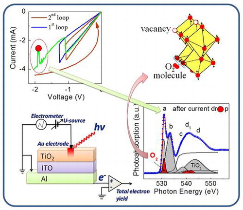
Electrophysical and NEXAFS studies were implemented in the same point of Al/ITO/TiO2 assembly (left bottom corner). The region of the current instability in the I-V characteristics was revealed. The current instability resulted in transition to a new hysteresis loop (left upper corner). A formation of the O2 molecules in the volume of TiO2 active layer has been established specifically in the region of current instability (right upper and bottom corners).
1. Introduction
Resistance-change random access memory (ReRAM) has attracted extensive attention as a promising candidate for non-volatile memory due to its high switching speed, high scalability, multi-bit storage potential and simple structure.[Citation1–14] The principle of operation of ReRAMs involves a functional dependence of resistance of the material on the charge passing through it [Citation15] that is realized in devices as resistive switching.[Citation16] There is consensus now that resistive switching is performed by the conductive filaments formation/rupture process in many systems, and the conductive filament model is now accepted extensively.[Citation3,4,17–21] Note that conductive filaments need to be initially formed in the insulator.[Citation22,23] However, there still exist some issues in ReRAM devices based on the filament formation/rupture process that are critical to guarantee the stability and reproducibility of the operations in the ReRAM. Currently, [Citation16,24–26]the possible causes for the lack of stability of resistance values in the low resistive state (RL) and high resistive state (RH) are being actively discussed.[Citation16,24–26] It is noted [Citation24,25,27] that the low resistance state is more stable than the high resistance state. According to the model proposed in [Citation28], the distribution of filaments in the switching matrix is generally random, allowing a large variation of switching voltages for different cells from time to time. One of the factors affecting the stability of the resistive switching is a microstructure of the active layer.[Citation29–31] In these references it was found that with increase of crystallinity (decrease of grain boundary density), the resistances and switching voltages become much more stable. According to [Citation32], the location and growth direction of the filaments are confined by the grain boundaries.
The goal of the current paper is a study of the stability of the resistive switching process in the Al/ITO/TiO2 (ITO is (In2O3)0.9(SnO2)0.1) assembly. Earlier [Citation33] we revealed that metal/TCO/TiO2 (TCO is a transparent conducting oxide) assemblies demonstrate the memristor effect after synthesis (without additional annealing) that provides progress towards understanding the nature of the memristor effect. Also it was established that after the switching process these structures can be retained for a long time. The production-grade Al wafer has been chosen as the substrate because of the specific morphology of its surface (grainy morphology). This allows us to analyze the effect of the surface morphology on the microstructure of the film and as a consequence on the stability of the resistive switching in the system. As a reference system the deg-Si/ITO/TiO2 assembly was used, where deg-Si is degenerate silicon substrate with atomically smooth surface and electrical properties nearly the same as those of a metal substrate. In order to gain insight into the electronic and atomic structure of the TiO2 film in addition to electrophysical investigations we have carried out near edge X-ray absorption fine structure (NEXAFS) spectroscopic studies of the assemblies after applying the electric field. We have studied the effect of the electric field at different stages, characterized by different values of current and voltage, on the atomic and electronic structure of assemblies. The NEXAFS arises from the excitations into unoccupied molecular orbitals. NEXAFS is dominated by multiple scattering of a low-energy photoelectron in the valence potential set up by the nearest surroundings. Spectral “fingerprint” techniques can be used to identify the local bonding environment. This fact defines the highest sensitivity of NEXAFS, to distinguish chemical bonds and nearest neighbors. Thus NEXAFS provides information about local (associated with a hole localization in the core shell) and partial (allowing for certain angular momentum symmetry) electronic density of states of the conduction band.
2. Experimental methods
TiO2 film of 20 nm thickness was grown by the atomic layer deposition (ALD) technique on production-grade Al and deg-Si wafers. ALD provides thickness control and aggressive conformality of TiO2 thin films at a reasonably low processing temperature. The TiO2 film was deposited in a cross-flow “Nanoserf” reactor at a temperature of 200°C using TiCl4, Ti[OCH(CH3)2]4, [(CH3)2 N]4Ti and H2O precursors. A homogeneous ITO buffer layer of thickness 100 nm was grown on the Al and deg-Si substrates prior to the ALD deposition of TiO2 film.
The surface topography of Al/ITO/TiO2 and deg-Si/ITO/TiO2 assemblies was examined with the helium ion microscope (HIM) at a chamber base pressure of 10−7 Torr. A focused beam of single-charged helium ions accelerated to 35 keV scanned over selected area of the sample. A beam current from 0.1 to 1 pA was used for imaging to avoid ion-induced sputtering of the sample. Images were obtained in the secondary electron detection mode with a conventional Everhart-Thornley detector. The high resolution transmission electron microscopy (HRTEM) images were obtained with a Carl Zeiss Libra 200 FE 200 keV microscope.
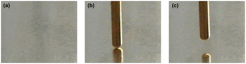
The I-V characteristics of the synthesized structures were measured at room temperature at ambient atmosphere using an original setup in the I-V sweep mode. The measurements were performed by applying a linearly varying voltage in the range of ±2 V to the top electrode with the bottom electrode grounded (Figure ); current was changed within ± 4 mA. The applied voltage allowed creation of an electric field of the order of 1 MV/cm in the TiO2 layer. The Au circular-shaped electrodes were used as external point contacts. The contact area was about 1 ×10⁻⁴ cm2. The electrode holder allowed contact with a constant clamp force. Measurement was performed in a few steps (Figure ): positioning of the electrode over measuring point, gentle landing of the electrode, carrying out desired sweeps/switching, lifting the electrode.
Figure 1. Schematic representation of electrophysical and NEXAFS measurements implemented at the same point of the sample.
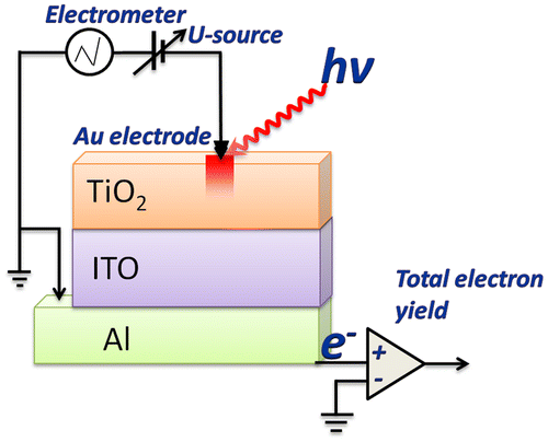
Figure 2. Photograph of the sample surface before and after electrode landing and retraction: sample placed on measuring table (a), electrode landed (b), electrode retracted (c). The diameter of electrode was about 1 mm, the contact area was about 1 × 10⁻⁴ cm2.
To study the atomic and electronic structure of the active layer of TiO2 at the point of impact of a high electric field (at the point of resistive switching) a special fiducial grid was applied on the surface of the sample, enabling measurement of the current-voltage characteristics and NEXAFS spectra in the same point of the film: the light spot on the sample was combined with contact area between the Au electrode and film TiO2. For this purpose the aluminum fiducial marks were deposited on the surface of pristine TiO2 by magnetron sputtering. All the marks were located on the same line.
The resistive switching in all the systems was performed outside the vacuum chamber of the spectrometer, in the air. Note that earlier [Citation33] the possibility of switching in the air in all the studied samples was confirmed by implementing the resistive switching in a specially designed box under a nitrogen atmosphere. The resistive switching processes were shown to be almost identical in ambient and nitrogen atmosphere. A specially designed table with a vernier was used. The system allowed the position of the Au electrode to be controlled: it could be mechanically moved along a straight line. The resistive switching was carried out at the points located midway between the Al marks.
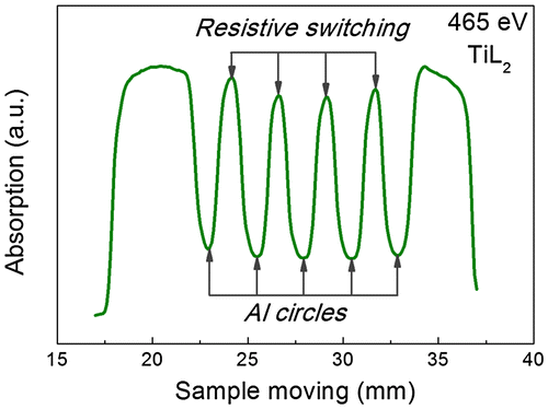
After that the sample was placed in the vacuum chamber of the spectrometer so that a straight line passing through the centers of marks were coincided with the line at which the light spot could move during the translation the sample holder. Note that it was possible to move the sample perpendicularly to the beam during the experiment without upsetting the vacuum; this has permitted different points on its surface to be studied. In order to align the scale of the Au electrode movement in air with movement of the sample in the vacuum chamber, the scanning all over the length of the sample was conducted at fixed photon energy. We used an energy of 465 eV, which corresponds to Ti L2,3 absorption edge where a strong absorption by titanium atoms occurs. An example of such a scan is shown in Figure . The minima on the curve correspond to the aluminum marks, and the maxima correspond to the TiO2 film located between labels.
Figure 3. The example of scanning over the length of the sample carried out at 465 eV. The energy 465 eV corresponds to the Ti L2,3 absorption edge where a strong absorption by titanium atoms occurs. The minima on the curve correspond to the aluminum marks, maxima correspond to the TiO2 film located between aluminum marks.
As a result the points at which the implementation of high electric field (resistive switching) was carried were established. Further, the Ti L2,3- and O K absorption spectra were measured at these points. Schematic representation of the idea of the experiment is shown in Figure .
The NEXAFS measurements were performed at the reflectometer set-up mounted on the optics beamline (D-08-1B2) of the Berlin Synchrotron Radiation facility BESSY-II of the Helmholtz Zentrum Berlin (HZB). A Hamamatsu GaAsP diode (4 x 4 mm window), together with a Keithley 617 electrometer, was used as a detector. NEXAFS spectra were measured at the incident angle of 45° in the vicinity of Ti L2,3 and O K absorption edges with energy resolution better than E/ΔE = 3000. The spectra were obtained by monitoring the total electron yield from the samples in a current mode. Apertures were used to narrow the area of the light spot on the film. Taking into account the size of X-ray beam which was 150 × 200 μm2 and the grazing incidence angle 45°, the size of the studied area was about 200 × 200 μm2. Thus the size of the studied area was approximately equal to the active area in which resistive switching occurs. It is important to emphasize that after applying the voltage the electrode was retracted from the film TiO2, and further NEXAFS measurements were carried out directly at the contact area at the TiO2 film without electrode. As a consequence, the obtained NEXAFS spectra provided information on changes in the electronic and atomic structure itself from the electric field impact area. The schematic representation of electrophysical and NEXAFS measurements is shown in Figure . The paper is focused on the Al/ITO/TiO2 assembly, which was studied before (as pristine) and after electric field effect. Additionally the deg-Si/ITO/TiO2 assembly was studied as a reference system.
3. Results and discussion
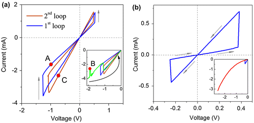
The stable reversible resistive switchings in the Al/ITO/TiO2 assembly were achieved by applying a linearly varying voltage. The stable hysteresis loop is shown in Figure (a) (blue curve). This state will be termed the first stable hysteresis loop. Only anti-clockwise bipolar resistive switching was realized. Since no instabilities were observed in the range of the stable hysteresis loop the sweep up to –2 V was performed beyond the voltage (–1.3 V) needed for the RL→RH transition. The instabilities of current started from the –1.7 V. It is important that a current drop had occurred at –1.9 V. The voltage was switched off at –2 V after the reverse current jump. The current instability resulted in transition to a new hysteresis loop that is shown in the inset in Figure (a) (brown curve). An initial state in the new loop was RL. The values of RL and RH had decreased in comparison with the values for the initial hysteresis loop. It should be noted that the values of RL and RH established for first and second stable hysteresis loops were repeatable many times (at least 15 times) with an uncertainty of ±0.5%.
Figure 4. I-V characteristics for the substrate/ITO/TiO2 assemblies (a) Al substrate; (b) deg-Si substrate. In panel (a) the blue curve is a first stable hysteresis loop. The brown curve is a second stable hysteresis loop obtained right after the current instabilities in the green curve (inset). The inset zooms into the region where the current instability occurs. The green curve is one sweep from 0 to –2 V after obtaining the first stable hysteresis loop, current instabilities were observed starting from –1.7 V. Both hysteresis loops were repeatable at least 15 times with uncertainty of 0.5%. The red circles in the curves denote the steps of I-V sweep on which the NEXAFS measurements were performed. A, RH state in the first loop; B, current drop in the region of instability; C, RL state in the second loop. Inset in the panel (b) shows the sweep beyond the stable hysteresis loop, no instabilities were observed.
It was plausible to assume that the process of the current instability was accompanied by irreversible changes in electronic and atomic structure of the TiO2 because the initial hysteresis loop was no longer obtainable. In order to gain insight into the electronic and atomic structure of the active TiO2 layer the NEXAFS study was conducted at different steps of the electric field effect, which are shown in Figure (a) by red circles. Note that the 20 nm thick film was studied. Taking into account the value of a probing depth (of the order of 7 nm) [Citation34,35] in the NEXAFS technique, it is obvious that we studied the processes occurring in the volume (closer to the surface) of the film but not at the interface between the TiO2 film and ITO. Actually we studied the response of the electronic and atomic structure of the film to the effect of electric field.
In the first step of the NEXAFS experiment the film (pristine structure) was studied at different points. The absorption spectra in the vicinity of Ti L2,3(2p) and O K(1s) absorption edges were measured (Figure (a) and (b)). It is important to emphasize that within the statistical error (in the order of 3%) the spectra measured at different points on the surface of the sample coincided.
Figure 5. (a) Ti L2,3 (2p)- and (b) O K (1s)-absorption spectra of the Al/ITO/TiO2 and deg-Si/ITO/TiO2 assemblies (pristine structure). The insets in panels (a) and (b) are zooms of features b-b′ and f respectively.
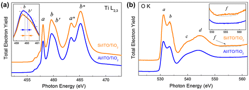
According to the classical conception, the NEXAFS excitation at the Ti 2p threshold in TiO2 occurs mainly within the octahedral environment of oxygen atoms and the Ti 2p absorption spectrum should reflect the energies of the free Ti 3d states, because it is dominated by the 2p → 3d dipole transitions in the Ti atoms.[Citation36] One can see that the Ti 2p absorption spectrum reflects clearly the spin-orbit splitting of the Ti 2p level. The Ti 2p1/2 structures are marked by asterisks in Figure (a). The peaks a and b in Ti 2p3/2 spectrum stem from dipole allowed transitions of Ti 2p3/2 electrons to unoccupied 3d states, which are split into 3dt2 g (peak a) and 3 deg (peak b) components by the octahedral crystal field created mainly by the O ions. The line shape analysis of the core-to-eg transitions attracts the highest attention in order to reveal the crystal modification of TiO2 film. The absence of the splitting the peak b (doubly degenerated eg component) indicates an amorphous state of the studied TiO2 film (Figure (a)). It should be noted that the Ti 2p- absorption spectra measured before and after the electric field effect were almost indistinguishable, which means the main changes of the structure occur in the sublattice of oxygen. Due to this reason only the O 1s-absorption spectra will be discussed further.
The relative intensities of all the O 1s-absorption spectra have been normalized to the continuum jump (at the photon energy of 560 eV) after subtraction of a sloping background, which was extrapolated from the linear region below O 1s-absorption onset. Such normalization provides about the same total oscillator strength for all the O 1s-absorption spectra over the photon energy range of 520–560 eV in accordance with a general idea of oscillator strength distribution for the atomic X-ray absorption.[Citation36]
Figure (b) shows the O 1s-absorption spectrum of the pristine structure of the TiO2 film. According to [Citation37–40], the molecular orbitals of TiO2 derived from a linear combination of atomic orbitals (LCAO) are characterized by four unoccupied orbitals: 2t2 g, 3eg, 3a1 g and 4t1u. In TiO2, which has zero d-electrons, all four molecular orbitals are completely empty. In this classification the O 1s-edge features (labeled as a, b, c and d) can be assigned to one electron transition from the O 1s orbital to the 2t2 g, 3eg, 3a1 g and 4t1u orbitals of TiO2, respectively. Thus a and b peaks reflect the core-electron transitions in the oxygen atoms to the lowest unoccupied Ti 3dt2 g and 3 deg electronic states that are mixed with the 2p states of the ligand (oxygen) atoms. The analysis of the energy position of the peaks shows that within the experimental accuracy (10 meV) the energy separation between a and b peaks is equal to 2.3 eV, which correlates well with the value for amorphous TiO2.[Citation41,42] It is important to stress that according to [Citation40] the feature c originates from the states, which are dominated by oxygen 2p character and they are best assigned as antibonding combinations of direct oxygen–oxygen interactions. The feature d can be assigned to titanium 4 sp band mixing with O 2p states. The absence of the feature at the 553 eV in the O 1s-absorption spectrum is additional evidence of the amorphous structure of the film.[Citation42–44]
As it has been mentioned in the introduction, according to the model proposed in [Citation28], the distribution of filaments in the switching matrix is generally random, which allows a large variation of switching voltages for different cells from time to time. One of the factors affecting the stability of the resistive switching is a microstructure of the active layer.[Citation29–31] These authors found that with increase of crystallinity (decrease of grain boundary density), the resistances and switching voltages become much more stable. According to [Citation32] the location and growth direction of the filaments are confined by the grain boundaries. Thus it is plausible to assume that amorphous structure of TiO2 film may be a reason for current instabilities observed.
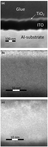
In order to gain further insight into a microstructure of TiO2 layer we have studied a surface topography of TiO2 film and Al substrate by helium ion microscopy (HIM) and high resolution transmission electron microscopy (HRTEM). The TEM image of Al/ITO/TiO2 assembly is shown in Figure (a). One can see that Al substrate has a pronounced surface relief with characteristic size no less than 20 nm. The ITO layer and TiO2 film replicate this relief. It is important that TiO2 film uniformly coats the surface without any discontinuity. The scaled HRTEM image in the area of TiO2 film is shown in Figure (b). No crystal order can be seen in the structure of the TiO2 film, which confirms its amorphous structure.
Figure 6. TEM image of Al/ITO/TiO2 assembly (a). Panels (b) and (c) show the HRTEM images of TiO2 film in Al/ITO/TiO2 and deg-Si/ITO/TiO2, respectively.
The HIM image of the surface topography of the TiO2 film deposited on Al substrate is shown in Figure (a). The surface of the TiO2 film formed on the Al substrate reveals a grainy morphology with size of grains in the range 20–30 nm. It is important that a clearly defined relief of the surface in the form of rolled strips is traced. The depth of the groove is no less than 10–15 nm and occasionally reaches the value of 20 nm. The surface of the Al substrate has the same morphology features, particularly rolled strips (Figure (b)). One can presume that such substrate relief causes the grainy structure of the TiO2 film, leading to the current instabilities.
Figure 7. HIM image of TiO2 film deposited on (a) Al/ITO and (c) deg-Si/ITO substrates and of an Al substrate (b) and a deg-Si substrate (d).
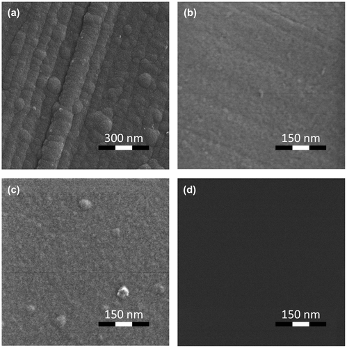
To support our idea that amorphous structure of the TiO2 film may be a reason for the observed current instabilities we have additionally studied the deg-Si/ITO/TiO2 assembly. The I-V characteristic for the deg-Si/ITO/TiO2 assembly is shown in Figure (b). No instability was observed in this system, either inside the hysteresis loop or beyond that, as is shown in the inset of Figure (b). As follows from Figure (c) the film grown on the deg-Si substrate shows a rather smooth uniform surface. Let us look at the Ti L2,3 absorption spectrum of this system in pristine state, shown in Figure (a). The spectrum of the film synthesized on deg-Si differs from the spectrum of film grown on the Al substrate in the contrast and the shape of the feature b (appearance of a shoulder b′). This doubling of the Ti 2p→3 deg transitions in TiO2 is well known [Citation40,41,43–45] and is a result of symmetry breaking on Ti atom, which is typical for different crystal modifications (anatase, rutile, and brookite) of TiO2. The manifestation of doubling of the Ti 2p→3 deg transitions depends on the crystalline structure of TiO2 and is expressed in the relative intensities of features b and b′. In anatase the intensity of feature b is substantially higher than intensity of the feature b′, while in rutile the opposite situation is observed.[Citation43,45] Analysis of Ti L2,3 absorption spectra allows us to assume the presence of signs of an ordered structure of the anatase type in the film synthesized on deg-Si, as the shoulder b′ is more pronounced for deg-Si/ITO/TiO2 (Figure (a) inset; the spectra shown here are normalized to the intensity of first peak a). One can see a decreasing intensity of features b-b′ relative to peak a for deg-Si/ITO/TiO2 assembly. According to [Citation46,47], the intensity of t2 g state (feature a) dominates over eg state (feature b-b′) in the Ti L2,3 absorption spectra of crystalline TiO2, while the opposite situation is observed for amorphous TiO2. Thus the higher intensity ratio of t2 g - eg components (features a and b-b′) may be considered as additional evidence of better order in TiO2 film in deg-Si/ITO/TiO2 assembly. The analysis of the shape of the O K absorption spectra of deg-Si/ITO/TiO2 and Al/ITO/TiO2 (Figure (b)) can further support our assumption. According to [Citation46,47], the higher intensity of peaks a and b in Figure (b), together with their narrower width and shift of feature d toward the higher energy side in comparison with Al/ITO/TiO2, also points to a better structural order of TiO2 film in deg-Si/ITO/TiO2 assembly. Finally, the presence of the broad and weak feature f in the O K absorption spectrum of the TiO2 film grown on the deg-Si is an evidence of signs of ordered structure of the anatase type in this film.[Citation40] In view of the electrophysical studies mentioned above, one can conclude the correlation exists between the crystallinity of the film structure and resistances and switching voltages stability that agrees well with [Citation29–32].
Further, the film was studied after the electric field effect. The red circles in the I-V curves in Figure (a) denote the following steps of I-V sweep on which the NEXAFS measurements were performed: A denotes the RH state in the first loop, B was chosen in the range of current instability, specifically after a current drop, and C was chosen after a reverse current jump, which had caused RL state at new hysteresis loop.
Figure shows the O 1s-absorption spectra of the TiO2 film at the different steps of the electric field effect. In order to enable a comparison of the spectral features, the relative intensities of the spectra have been normalized to the same continuum jump at the photon energy of 560 eV, after subtraction of a sloping background, which was extrapolated from the linear region below the O 1s absorption onset. Such normalization provides about the same total oscillator strength for all the O 1s-absorption spectra over the photon energy range of 525–560 eV, in accordance with a general idea of oscillator strength distribution for the atomic X-ray absorption.[Citation36] As it follows from Figure the spectra correlate well in number and energy position with the main features of the fine structure. At the same time a clear change of the integrated intensity of peak a before and after inducing the electrical filed can be traced. Two different tendencies can be noticed. A significant intensity decrease is observed for peaks a and b depending on the step in orderly sequence: pristine structure, RH state at first hysteresis loop (after electroforming) (A), and in the RL state at second hysteresis loop (C). Contrary to these spectra the peak intensity a increases considerably and peak d1 arises in the spectrum corresponding to the current drop (B) in the region of the current instability at the I-V characteristic.
Figure 8. O K (1s)-absorption spectra of the Al/ITO/TiO2 assembly measured at different stages of the electric field effect, characterized by different values of current and voltage: 1, pristine structure; 2, RH state at first hysteresis loop (after electroforming); 3, after current drop in the region of current instability; 4, RL state at second hysteresis loop. The negative polarity of bias was used.
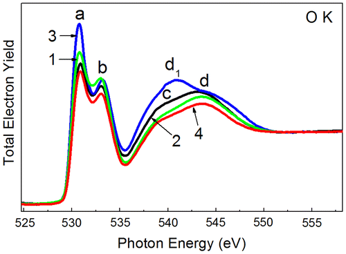
Let us consider jointly the measured O 1s-absorption spectra and I-V characteristics. When a high electric field is applied to pristine structure (electroforming process) the oxygen atoms are knocked out from the lattice and move to the electrode with the positive voltage creating defects that causes formation of the conducting levels in the band gap. Note that in octahedral complexes the metal eg orbitals (peak b) are directed toward the oxygen atoms and have a strong overlap with the oxygen 2p orbitals. As a result, the O 1s-near edge structure is very sensitive to changes in the local environment of Ti atom.[Citation43,48,49] The above-mentioned change of the integrated intensity of peak a before and after inducing the electrical field (decrease of the integrated intensity of peak a after electroforming process) together with the results of studies [Citation48,49], according to which the peak a of the O 1s-absorption spectrum strongly depends on the concentration of oxygen vacancies, support the physical model of the electroforming process.
As follows from Figure (4th curve), a subsequent decrease of the resistance (transition to RL state at second hysteresis loop) is also accompanied by some decrease of the peaks intensity a and b. It is plausible to assume that this transition is connected with further the oxygen atoms leaving the lattice and formation of the oxygen vacancies under the action of the electric field. The electric field stimulates the directed oxygen ions drift from the region of the formed vacancy localization, providing a spatial separation of the vacancy and oxygen ion preventing the possibility of reverse capture. The shift of the oxygen ions O2– can occur also due to diffusion that can be promoted by the local heating.
Figure (a) shows the O 1s-absorption spectrum of the TiO2 film measured after the current drop in the region of the instability at the I-V characteristic. The deconvolution of the spectrum performed using free software “Athena” [Citation50] is also shown. The symmetrical Gaussian shape of peaks was used. The continuous edge jump at ionization potential has been represented by the arctangent function. The position of edge jump 536 eV was estimated from sum of O1s binding energy [Citation52] and work function [Citation53] in TiO2. It can be seen from the presented deconvolution that the discussed spectrum is a sum of two spectra. The first one correlates with the spectrum of amorphous TiO2.[Citation41,42] The second spectrum demonstrates the presence of a localized narrow peak and four rather wide peaks. The first narrow peak correlates well in width and energy position with the first sharp resonance in absorption spectra of molecular O2 presented in [Citation51,55] which is due to1σu→1πg* transition. The spectra of molecular O2 contain the second relatively broad doublet band which is related to the 1σg→3σu* excitation. Doubling of this band results from the spin-up and spin-down configurations in the final state. The doubling of this band and its relative intensity depend on the state of O2 but it is essential that the energy position of the center of the σ* band is not changed for gas-phase O2, condensed or physisorbed O2 on the metal surface. A resulting curve for sum of π* and σ* peaks in deconvolution of spectrum measured in the region of current instability (Figure (a)) is shown in Figure (b) in comparison with the spectra of gas-phase O2 and O2 physisorbed on Pt(111) from [Citation51]. It is important that the center of σ* band in the resulting envelope curve is almost the same as that in the presented spectra of gas-phase O2 and physisorbed O2. This allows us to affirm that molecular O2 is being formed in the TiO2 bulk during current instabilities. The absence of actual doubling of the σ* band in the resulting envelope curve may indicate that not exactly gaseous O2 is being formed in TiO2 at the moment of current instability but some intermediate form of O2. The bond length is almost the same for the intermediate and gaseous O2 forms and these intermediate O2 molecules are not chemically bonded to TiO2 matrix, as the energy separation between π* and σ* bands and the shape of σ* band are significantly different for lengthened O2 molecules as it takes place in case of chemisorbed oxygen.[Citation51] A formation of titanium dioxide molecule dimers (TiO2)2 seems also not to be the case. It is shown in [Citation56] that titanium dioxide molecule dimers have symmetry significantly lower than TiO6 octahedra. Changing the symmetry of Ti surroundings would surely provoke changing the shape of Ti L2,3 absorption spectra but actually the shape of those was almost unchanged at all studied stages of electric field effect, as mentioned above.
Figure 9. (a) O 1s-absorption spectrum of the Al/ITO/TiO2 assembly measured in the region B after current drop in the region of the current instability. The deconvolution of the spectrum was performed using the free software “Athena” [Citation50]. Green peaks correspond to t2 g, eg, a1 g, and t1u states of TiO2; red peaks correspond to π* and σ* states of molecular oxygen. (b) 1 and 2, O 1s-absorption spectra of molecular oxygen in gas-phase and physisorbed on Pt(111) respectively from [Citation51]; 3, a resulting curve for sum of π* and σ* peaks of molecular oxygen in deconvolution of O 1s-absorption spectrum shown in (a).
![Figure 9. (a) O 1s-absorption spectrum of the Al/ITO/TiO2 assembly measured in the region B after current drop in the region of the current instability. The deconvolution of the spectrum was performed using the free software “Athena” [Citation50]. Green peaks correspond to t2 g, eg, a1 g, and t1u states of TiO2; red peaks correspond to π* and σ* states of molecular oxygen. (b) 1 and 2, O 1s-absorption spectra of molecular oxygen in gas-phase and physisorbed on Pt(111) respectively from [Citation51]; 3, a resulting curve for sum of π* and σ* peaks of molecular oxygen in deconvolution of O 1s-absorption spectrum shown in (a).](/cms/asset/22871779-bbec-47b6-90e0-8339ebd28241/tsta_a_1182851_f0009_oc.gif)
The formation of O2 molecules was indirectly indicated in a number of studies [Citation57–60] by means of observation of bubbles on the surface of the top electrode of some assemblies after resistive switching. All knowledge of the occurrence of oxygen gas has till now been obtained from scanning electron microscopy (SEM) or atomic force microscopy (AFM) images and does not give a clear idea at which specific stage of the switching process the formation of molecular oxygen occurs. One can see from our result that the O2 molecules are formed exactly in the region of instability of current because neither the O 1s-absorption spectrum after electroforming nor that for RL state in the second loop contains the contribution of O2 molecules (Figure ). One can see that the influence of electric field on the film in this region leads to formation of the molecular oxygen that is accompanied by the momentary decrease of the current (Figure (a)).
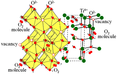
In our opinion the observed phenomenon is a manifestation of the joint action of electric field and local heating (self-heating), where the dominant mechanism is heating, wrenching the oxygen atoms off the regular bonds with formation of the oxygen vacancies. In reality the further increase of the voltage up to the region of instability leads to the increase of the amplitude of the oxygen atoms vibrations due to electrical Joule heating and as a result to the creation of the O2 molecules. We have established that the observed current instability does not depend on the direction of the electric field, which confirms our supposition. The instability occurs at a voltage specific to the system. Exactly at these voltages the creation of the O2 molecules occurs. Figure summarizes the described processes and gives a schematic presentation of the formation of the O2 molecules in the Al/ITO/TiO2 assembly.
Figure 10. Schematic presentation of the oxygen atoms leaving the lattice, formation of the oxygen vacancies under the action of electric field and local heating and formation of the O2 molecules in the Al/ITO/TiO2 assembly.
4. Conclusions
We have characterized an Al/ITO/TiO2 assembly, where a TiO2 layer of 20 nm thickness was grown by ALD. The electric field effect on the TiO2 structure was studied by NEXAFS in addition to electrophysical measurements. We have observed current instability in the I-V characteristics and have shown its independence on the direction of the electric field. It has been revealed that this current instability is supported by the amorphous structure of the TiO2 film but is initiated by the surface morphology of the Al substrate. A formation of the O2 molecules in the TiO2 active layer has been established specifically in the region of current instability. The formation of the oxygen bubbles on the surface of the top electrode of some assemblies during resistive switching was reported in [Citation57–60]. All the knowledge of occurrence of oxygen gas has until now been obtained from SEM or AFM images and does not give a clear idea at which specific stage of the switching process the formation of molecular oxygen occurs. It has been only noted that the occurrence of the bubbles impedes the stable reversible resistance switching.
In the present studies we have directly observed formation of the O2 molecules using NEXAFS spectroscopy and have shown that formation of the O2 molecules occurs specifically in the region of the current instability as a result of electrical Joule heating manifestation. The obtained results are very important for a deeper understanding of the mechanism of resistance switching and charge transport in TiO2 films and its future application as switching material in resistance change memory based devices.
Funding
This work was supported by the Helmholtz-Zentrum Berlin
Acknowledgments
The work was supported by St Petersburg State University [grant 11.37.656.2013]. The authors gratefully acknowledge the financial support of Helmholtz Zentrum Berlin (HZB) and also thank HZB for the allocation of synchrotron radiation beamtime. The work was performed using equipment of interdisciplinary resource center for “Nanotechnology” and resource center “Innovative technologies of composite nanomaterials” of St Petersburg State University.
Disclosure statement
No potential conflict of interest was reported by the authors.
References
- Szot K, Speier W, Bihlmayer G, et al. Switching the electrical resistance of individual dislocations in single-crystalline SrTiO3. Nat Mater. 2006;5:312–320. 10.1038/nmat1614
- Terabe K, Hasegawa T, Nakayama T, et al. Quantized conductance atomic switch. Nature. 2004;433:47–50.
- Waser R, Aono M. Nanoionics-based resistive switching memories. Nat Mater. 2007;6:833–840. 10.1038/nmat2023
- Sawa A. Resistive switching in transition metal oxides. Mater Today. 2008;11:28–36. 10.1016/S1369-7021(08)70119-6
- Yi HT, Choi T, Cheong S-W. Reversible colossal resistance switching in (La,Pr,Ca)MnO3: Cryogenic nonvolatile memories. Appl Phys Lett. 2009;95:063509–63511. 10.1063/1.3204690
- Watanabe Y, Bednorz JG, Bietsch A, et al. Current-driven insulator–conductor transition and nonvolatile memory in chromium-doped SrTiO3 single crystals. Appl Phys Lett. 2001;78:3738–3740. 10.1063/1.1377617
- Beck A, Bednorz JG, Gerber CH, et al. Reproducible switching effect in thin oxide films for memory applications. Appl Phys Lett. 2000;77:139–141. 10.1063/1.126902
- Liu SQ, Wu NJ, Ignatiev A. Electric-pulse-induced reversible resistance change effect in magnetoresistive films. Appl Phys Lett. 2000;76:2749–2751. 10.1063/1.126464
- Choi BJ, Jeong DS, Kim SK. Resistive switching mechanism of TiO2 thin films grown by atomic-layer deposition. J Appl Phys. 2005;98:033715–33724. 10.1063/1.2001146
- Wu X, Zhou P, Li J, et al. Reproducible unipolar resistance switching in stoichiometric ZrO2 films. Appl Phys Lett. 2007;90:183507–183509. 10.1063/1.2734900
- Xu N, Liu LF, Liu XY, et al. Characteristics and mechanism of conduction/set process in TiN∕ZnO∕Pt resistance switching random-access memories. Appl Phys Lett. 2008;92:232112–232114. 10.1063/1.2945278
- Rohde C, Choi BJ, Jeong DS, et al. Identification of a determining parameter for resistive switching of thin films. Appl Phys Lett. 2005;86:262907–262909. 10.1063/1.1968416
- Choi BJ, Choi S, Kim KM, et al. Study on the resistive switching time of TiO2 thin films. Appl Phys Lett. 2006;89:012906–12908. 10.1063/1.2219726
- Rossel C, Meijer GI, Bremaud D, et al. Electrical current distribution across a metal–insulator–metal structure during bistable switching. J Appl Phys. 2001;90:2892–2898. 10.1063/1.1389522
- Strukov DB, et al. The missing memristor found. Nature. 2008;453:80–83. 10.1038/nature06932
- Meijer GI. Who Wins the Nonvolatile Memory Race. Science. 2008;319:1625–1626. 10.1126/science.1153909
- Kwon D-H, et al. Atomic structure of conducting nanofilaments in TiO2 resistive switching memory. Nat Nanotechnol. 2010;5:148–153. 10.1038/nnano.2009.456
- Soni R, Meuffels P, Kohlstedt H, et al. Reliability analysis of the low resistance state stability of Ge0.3Se0.7 based solid electrolyte nonvolatile memory cells. Appl Phys Lett. 2009;94:123503–123505. 10.1063/1.3103555
- Schindler C, Staikov G, Waser R. Electrode kinetics of Cu–SiO2-based resistive switching cells: Overcoming the voltage-time dilemma of electrochemical metallization memories. Appl Phys Lett. 2009;94:072109–72111. 10.1063/1.3077310
- Russo U, Kamalanathan D, Ielmini D, et al. Study of Multilevel Programming in Programmable Metallization Cell (PMC) Memory. IEEE Trans Electron Devices. 2009;56:1040–1047. 10.1109/TED.2009.2016019
- Chang SH, et al. Effects of heat dissipation on unipolar resistance switching in capacitors. Appl Phys Lett. 2008;92:183507–183509. 10.1063/1.2924304
- Choi SJ, Park GS, Kim KH, et al. In Situ Observation of Voltage-Induced Multilevel Resistive Switching in Solid Electrolyte Memory. Adv Mater. 2011;23:3272–3277. 10.1002/adma.201100507
- Waser R, Dittmann R, Staikov G, et al. Redox-Based Resistive Switching Memories – Nanoionic Mechanisms, Prospects, and Challenges. Adv Mater. 2009;21:2632–2663. 10.1002/adma.v21:25/26
- Yang YC, Pan F, Zeng F. Bipolar resistance switching in high-performance Cu/ZnO:Mn/Pt nonvolatile memories: active region and influence of Joule heating. New J Phys. 2010;12:023008–23018. 10.1088/1367-2630/12/2/023008
- Yang M, Pei-Jian Z, Zi-Yu L, et al. Enhanced resistance switching stability of transparent ITO/TiO2/ITO sandwiches. Chin Phys B. 2010;19:037304–37308. 10.1088/1674-1056/19/3/037304
- Wang L-G, Qian X, Cao Y-Q, et al. Excellent resistive switching properties of atomic layer-deposited Al2O3/HfO2/Al2O3 trilayer structures for non-volatile memory applications. Nanoscale Res Lett. 2015;10:254028–142. 10.1186/s11671-015-0846-y
- Xu J, Yang Z, Zhang Y, et al. Bipolar resistive switching behaviours in ZnMnO film deposited on p-Si substrate by chemical solution deposition. Bull Mater Sci. 2014;37:1657–1661. 10.1007/s12034-014-0731-9
- Chae SC. Random Circuit Breaker Network Model for Unipolar Resistance Switching. Adv Mater. 2008;20:1154–1159. 10.1002/adma.v20:6
- Zhu X-J, Shang J, Li R-W. An overview of materials issues in resistive random access memory. Front Mater Sci. 2012;6:183–206.
- Lanza M, Zhang K, Porti M, et al. Grain boundaries as preferential sites for resistive switching in the HfO2 resistive random access memory structures. Appl Phys Lett. 2012;100:123508–123511. 10.1063/1.3697648
- Lanza M, Bersuker G, Porti M, et al. Resistive switching in hafnium dioxide layers: Local phenomenon at grain boundaries. Appl Phys Lett. 2012;101:193502–193506. 10.1063/1.4765342
- Zhuge F, Peng S, He C, et al. Improvement of resistive switching in Cu/ZnO/Pt sandwiches by weakening the randomicity of the formation/rupture of Cu filaments. Nanotechnol. 2011;22:275204–275210. 10.1088/0957-4484/22/27/275204
- Filatova EO, Baraban AP, Konashuk A, et al. Transparent-conductive-oxide (TCO) buffer layer effect on the resistive switching process in metal/ TiO2/TCO/metal assemblies. New J Phys. 2014;16:113014–113029. 10.1088/1367-2630/16/11/113014
- Stöhr J. NEXAFS Spectroscopy. Berlin: Springer; 1992. 10.1007/978-3-662-02853-7
- Hähner G. Near edge X-ray absorption fine structure spectroscopy as a tool to probe electronic and structural properties of thin organic films and liquids. Chem. Soc. Rev. 2006;35:1244–1255. 10.1039/B509853J
- Fano U, Cooper JW. Spectral Distribution of Atomic Oscillator Strengths. Rev Mod Phys. 1968;40:441–507. 10.1103/RevModPhys.40.441
- Fischer DW. X-Ray Band Spectra and Molecular-Orbital Structure of Rutile TiO2. Phys Rev B. 1972;5:4219–4226. 10.1103/PhysRevB.5.4219
- Stoyanov E. The effect of valence state and site geometry on Ti L3,2 and O K electron energy-loss spectra of TixOy phases. Am. Mineral. 2007;92:557–586.
- Groot FMF, Figueiredo MO, Basto MJ, et al. 2p X-ray Absorption of Titanium in Minerals. Phys Chem Miner. 1992;19:140–147. 10.1007/BF00202101
- Groot FMF, Faber J, Michiels JJM, et al. Oxygen 1s x-ray absorption of tetravalent titanium oxides: A comparison with single-particle calculations. Phys Rev B. 1993;48:2074–2080. 10.1103/PhysRevB.48.2074
- Rath S, Gracia F, Yubero F, et al. Angle dependence of the O K edge absorption spectraof TiO2 thin films with preferential texture. Nucl Instrum Methods Phys Res B. 2003;200:248–254. 10.1016/S0168-583X(02)01686-5
- Filatova E, Taracheva E, Shevchenko G, et al. Atomic ordering in TiO2 thin films studied by X-ray reflection spectroscopy. Phys Status Solidi B. 2009;246:1454–1458. 10.1002/pssb.v246:7
- Brydson R, Sauer H, Engel W, et al. Electron energy loss and X-ray absorption spectroscopy of rutile and anatase: a test of structural sensitivity. J Phys: Condens Matter. 1989;1:797–812.
- Groot FMF, Fuggle JC, Thole BT, et al. L2,3 x-ray-absorption edges of d0 compounds: K+, Ca2+, Sc3+, and Ti4+ in Oh (octahedral) symmetry. Phys Rev B. 1990;41:928–937. 10.1103/PhysRevB.41.928
- Ruus R, Kikas A, Saar A, et al. Ti 2p and O1s X-ray absorption of TiO2 polymorphs. Solid State Commun. 1997;104:199–203. 10.1016/S0038-1098(97)00300-1
- Kucheyev SO, Buuren T, Baumann TF, et al. Electronic structure of titania aerogels from soft x-ray absorption spectroscopy. Phys Rev B. 2004;69:245102–245108. 10.1103/PhysRevB.69.245102
- Casu MB, Braun W, Bauchspieß K R, et al. A multi-technique investigation of TiO2 films prepared by magnetron sputtering. Surf Sci. 2008;602:1599–1606. 10.1016/j.susc.2008.02.030
- Filatova EO, Sokolov A A, Egorova Yu V, et al. X-ray spectroscopic study of SrTiOx films with different interlayers. J Appl Phys. 2013;113:224301–224309. 10.1063/1.4809978
- Muller DA, Nakagawa N, Ohtomo A, et al. Atomic-scale imaging of nanoengineered oxygen vacancy profiles in SrTiO3. Nature. 2004;430:657–661. 10.1038/nature02756
- Ravel B, Newville, ATHENA, ARTEMIS, HEPHAESTUS: data analysis for X-ray absorption spectroscopy using IFEFFIT. J Synchrotron Radiat. 2005;12:537–541. 10.1107/S0909049505012719
- Chen JG. NEXAFS investigations of transition metal oxides, nitrides, carbides, sulfides and other interstitial compounds. Surf Sci Rep. 1997;30:1–152. 10.1016/S0167-5729(97)00011-3
- Gouttebaron R, Cornelissen D, Snyders R, et al. XPS study of TiOx thin films prepared by d.c. magnetron sputtering in Ar–O2 gas mixtures. Surf Interface Anal. 2000;30:527–530. 10.1002/(ISSN)1096-9918
- Diebold U, Madey TE. TiO2 by XPS. Surf Sci Spectra. 1998;4:227–231.
- Scanlon DO, Dunnill C W, Buckeridge J, et al. Band alignment of rutile and anatase TiO2. Nat Mater. 2013;12:798–801. 10.1038/nmat3697
- Kuiper P, Dunlap B. The σ* absorption peak at the oxygen 1s edge of O2: Exchange splitting, ultrafast dissociation, and atomiclike Auger spectra. J Chem Phys. 1994;100:4087–4092. 10.1063/1.466346
- Dargouthi S, Boughdiri S, Tangour B. Stabilizing of the Transitory Species (TiO2)2 by Encapsulation Into Carbon Nanotubes. Acta Chim Slov. 2015;62:445–451. 10.17344/acsi.2014.1080
- Kwon D-H, et al. Atomic structure of conducting nanofilaments in TiO2 resistive switching memory. Nat Nanotechnol. 2010;5:148–153. 10.1038/nnano.2009.456
- Yang JJ, Miao F, Pickett M D, et al. The mechanism of electroforming of metal oxide memristive switches. Nanotechnol. 2009;20:215201–215210. 10.1088/0957-4484/20/21/215201
- Huang J-J, Kuo C-W, Chang W-C, et al. Transition of stable rectification to resistive-switching in Ti/TiO2/Pt oxide. Appl Phys Lett. 2010;96:262901–262904. 10.1063/1.3457866
- Mehonic A, Buckwell M, Montesi L, et al. Structural changes and conductance thresholds in metal-free intrinsic SiOx resistive random access memory. J Appl Phys. 2015;117:124505–124513. 10.1063/1.4916259