
 ?Mathematical formulae have been encoded as MathML and are displayed in this HTML version using MathJax in order to improve their display. Uncheck the box to turn MathJax off. This feature requires Javascript. Click on a formula to zoom.
Abstract
We present a study of the electrical and magnetic properties of the amorphous Ge1-xMnx.DMS, with 2% ≤ x ≤ 17%, by means of SQUID magnetometry and low temperature DC measurements. The thin films were grown by physical vapour deposition at 50°C in ultrahigh vacuum. The DC electrical characterizations show that variable range hopping is the main mechanism of charge transport below room temperature. Magnetic characterization reveals that a unique and smooth magnetic transition is present in our samples, which can be attributed to ferromagnetic percolation of bound magnetic polarons.
1. Introduction
Diluted magnetic semiconductors (DMS) are a class of materials in which a magnetically inert host semiconductor (Ge, GaAs, CdTe or ZnSe) is doped with localized spins and carriers, either electrons or holes that are either itinerant or localized at the impurity sites. The possibility of combining the tunability of a semiconductor with the common properties of magnetic materials has been recognized as a promising route to explore new functionalities. Among the semiconductor materials showing ferromagnetic features, germanium manganese (Ge1-xMnx) diluted alloys have attracted attention since the discovery reported in 2002 by Park et al. [Citation1] of ferromagnetic order in a thin epitaxial layer of Mn-doped Ge. This attention is due mainly to the huge variety of magnetic behaviour that is linked to the tendencies of the transition metal ions to segregate in the semiconductor host, forming nanoclusters or nanocolumns, which are themselves ferromagnetic.[Citation2] Less work has been devoted to the study of the amorphous phase,[Citation3–6] which represents an interesting route to circumvent the issue represented by the formation of precipitates. These are very small crystallites that form when the DMS is grown at relatively high temperatures during epitaxial growth processes (typically by molecular beam epitaxy). These crystallites could be easily detected through the magnetic characterization because they display a well-defined Curie temperature, usually much higher than that of the diluted phase, e.g. in the case of Ge1-xMnx DMS, (Ge3Mn5) and
(Ge8Mn11).[Citation7,8]
In recent decades diluted magnetic alloys, such as Fe or Mn dispersed in Cu, have been extensively studied.[Citation9,10] In these metallic alloys, the low-density spins could be treated as a perturbation of the Fermi liquid, representing the host non-magnetic metal. Depending on the concentration of the impurities they could be studied in terms of Kondo systems or amorphous magnetic systems, with the spin–spin coupling mediated by the Ruderman–Kittel–Kasuya–Yosida interaction, which often leads to spin glass behaviour. To describe an insulating DMS system such as amorphous Ge1-xMnx the low carrier density regime (LCDR), in which the ratio between local moments over carriers is inverted with respect to the case of diluted magnetic alloys, is more appropriate to describe the behaviour of the system. In this scenario, the spin could not be treated as a perturbation of Hamiltonian for the charge carriers.[Citation11] As a consequence of the low moment density, the standard direct exchange between local moments (or superexchange) is not the dominant one; the exchange interaction is mediated mainly by localized carriers, despite their low concentration.
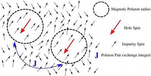
The most studied and accepted theoretical model for DMS in LCDR is based on the concept of bound magnetic polaron (BMP).[Citation11–13] At fairly low temperatures the localized holes (or electrons) start to polarize a cloud of neighbouring spins, due to the so-called Fermi contact interaction.[Citation13] The radius of such a BMP increases logarithmically with decreasing temperature. Consequently, one expects that long range ferromagnetic order appears in the system for temperatures low enough to allow formation of a continuous percolating network of BMP, if neighbouring BMPs prefer to orient ferromagnetically, depending this mainly on the interpolaron distance.[Citation13] These mechanisms favouring the stabilization of the single polaron and the parallel orientation of the BMP’s magnetic moments at low temperatures are both rather weak, and the resulting Curie temperatures, below which the long-range ferromagnetism is observed in these systems, are very low. In addition, the percolative nature of the transition implies that only a small fraction (∼20%) of the impurity spins participates to the ferromagnetic phase.[Citation11] The other, weakly interacting, spins remain unpolarized and, as a result, a substantial part of the spin entropy survives down to the low T-range.
In addition, magnetic moments are supposed to be randomly distributed in diluted magnetic semiconductors. As a consequence, it is possible in principle to find some regions inside the semiconductor where the density of the magnetic impurities is larger than the average value (as clusters). The carrier wave functions are pulled into those regions, where they can more effectively minimize their total energy. The increased probability of finding charge carriers in these smaller volumes leads to larger coupling of the localized spins inside the cluster. On the other hand, in a perfectly ordered DMS, carriers, due to the translational invariance, polarize equally all the impurities spins and this could happen only at very low temperatures, due to the small number of holes compared with the number of spins.
In this work, amorphous Ge1-xMnx in form of thin films in which Mn simultaneously provides both holes and localized spins are studied being an attractive prototypical material for several reasons. Firstly, the amorphous phase can be grown at low temperatures, avoiding in this way the formation of secondary phases. Secondly, the presence of precipitates can be detected in situ by using reflection high energy electron diffraction (RHEED), if a consistent fraction of the sample volume is constituted by these crystalline precipitates. Finally, doping of amorphous germanium with transition metals,[Citation14] due to the presence of dangling bonds, sets the conditions in the impurity band on the metallic side of the Mott transition. In this way it is possible to observe the property of a half full band with localization only due to disorder.[Citation15]
This will allow for a deeper insight into the mechanism of carrier-mediated magnetic ordering of the material, which can be hindered by the superposition of different ferromagnetic components in the crystalline counterpart.[Citation7] To this aim, a comparison of electrical and magnetic properties from different aGe1-xMnxsamples grown at increasing Mn content has been carried out. Then the results are compared with the relevant existing theoretical model.[Citation16] The proposed approach will provide the possibility to extract the localization length for the confined charge carriers in such highly disordered system.
2. Experiment
Two sets of amorphous aGe1-xMnxfilms were grown by physical vapour deposition using a molecular beam epitaxy apparatus () on oxidized silicon substrates, using an e-beam source for Ge and a Knudsen effusive cell for Mn. The first set of samples was grown without the presence of a cap layer, in order to perform electrical characterization and compositional analysis via X-ray photoemission spectroscopy (XPS). The second set was grown with a thin cap and a buffer layer of pure amorphous Ge in order to avoid contaminations from the substrate and oxidation in air after taking the sample out of the deposition chamber. All the other deposition parameters (substrate type and temperature, and rate of growth) are summarized in Tables and . The Mn flux was carefully tuned through the XPS compositional measurements of the first samples set and the Ge deposition rates were measured and kept constant using a calibrated quartz crystal microbalance. The RHEED pattern was continuously checked during the growth process to avoid any deviations from a uniform halo, characteristic of an amorphous structure. In addition grazing incidence X-ray diffraction (GIXRD) was performed ex situ which has highlighted only the presence of an amorphous phase for these samples; excluding the existence of small crystalline precipitates, in the detection limit of our XRD set-up.
Table 1. Growth parameters for the first set of aGeMn samples (for electrical characterization). All the parameter listed in the upper part of the table remain unchanged for the whole set. Thickness was measured by cross-sectional scanning electron microscopy.
Table 2. Growth parameters for the second set of aGeMn samples (for magnetic characterization). All the parameters listed in the upper part of the table remain unchanged for the whole set. Thickness was measured by profilometry.
The electrical measurements were performed on the first set of samples (Table ) in four point probe configuration using a Keithley® 2400 Source-Meter (Keithley, Solon, OH, USA) in a Janis® ST-100 H modified cryostat (Janis, Warburn, MA, USA),[Citation17] down to 80 K. The temperature is stabilized using a Lake-Shore® 331 Heater (Lake-Shore, Westerville, OH, USA) and a platinum resistance thermometer Pt-100 (unknown, PT100 standard thermistor) positioned near the sample on the copper holder. The macroscopic electrical contact to the sample was realized via argon sputter deposition of four Al strips (1 mm × 5 mm) using a mechanical mask to define the geometry. The dependence of the electrical resistance with T was extracted from the ohmic portion of the I-V characteristics.
The samples from the second set were subjected to magnetic measurements using a SQUID-VSM MPMS 3 by Quantum Design® (Quantum Design, San Diego, CA, USA). The hysteresis loops were taken from 2.5 K to 300 K in the field range. A SQUID magnetometer is very sensitive to small variation of magnetic flux reaching a sensitivity of 10−8 emu, but it measures all the contributions to the magnetic moment coming from the whole sample volume and sample holder. Therefore, a careful measurement of the magnetization curves of the bare substrate in the whole temperature range is required, in order to distinguish the contributions from the substrate and the film. P-type silicon substrates used in this work exhibit a diamagnetic susceptibility (negative slope of the M vs. H curve) in the whole temperature range, which decreases with cooling down and reaches a minimum at 2.5 K. This effect could be attributed to the paramagnetic susceptibility of the doping boron atoms. The contribution of the substrate is therefore subtracted to the moment of the three different samples after normalization to their respective mass, evaluated by means of precision gravimetric measurements. The value of the magnetic moment per unit of volume is obtained using the same gravimetric measurements, once the thicknesses of the deposited thin films and of the substrates are known. In the same temperature range, the field cooled – zero field cooled (FC-ZFC) curves were also collected by using the following procedure: the sample, as well as the superconducting magnet, was demagnetized at 300 K with an oscillating field of progressively decreasing amplitude, starting with a vertex value of 7 T. Then, temperature is lowered to 2.5 K with an applied field of H = 0 Oe and then the magnetic moment measurement was performed during warming up to room temperature under the application of a field of 50 Oe (ZFC). Then, the sample was demagnetized again at 300 K and brought down to 2.5 K with the same applied field, and finally the magnetic moment was measured again during the warming up in the same conditions (FC).
3. Results and discussion
3.1. DC electrical characterization
The results of the electrical characterization, reported in Figures and for the samples aGeMn1.2 (10%) and aGeM1.1 (2%) display an insulating behaviour and a relatively low conductivity due to both carrier compensation and strong degree of disorder. The electrical resistance grows with decreasing T according to a T−1/4 dependence, which is typical for the variable range hopping conduction regime.[Citation18] In a p-type amorphous semiconductor the electrical conduction at relatively low temperature is mainly dictated by hole hopping between localized states related to the impurity sites. The so-called nearest neighbour hopping mechanism assumes that the differences in energy of these states are small if compared with the thermal energy. The increase of the impurity concentration leads to the splitting of the localized levels and either the hopping range or the hopping probability at thermal equilibrium display an additional energy dependence, given by [Citation18]:
Figure 1. Electrical characterization. Values of electrical resistivity measured in the temperature range 80–300 K for the samples aGeMn1.1, aGeMn1.2, and in the temperature range 77–360 K for aGeMn1.3.
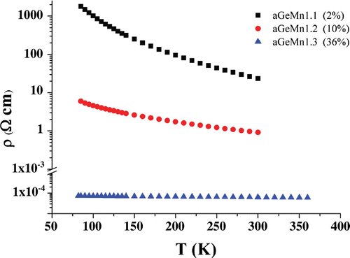
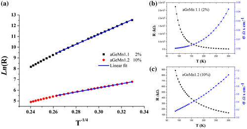
Figure 2. Electrical characterization (a) logarithm of the electrical resistance (R) plotted vs. T−1/4 for the sample aGeMn1.1 (squares) and aGeMn1.2 (circles); the solid lines are the linear fits of the experimental data. Right panels: electrical resistance in k (squares) and conductivity (dots) in vs. T (K) for aGeMn1.1 (b) and aGeMn1.2 (c).
(1)
(1)
where kB is the Boltzmann constant and a is the localization length of the holes wave functions. The hopping distance r for 3D systems depends on the temperature as described by [Citation18]:
(2)
(2)
where is the density of the states at the Fermi level. The corresponding activation energy for the process is given by:
(3)
(3)
Then, as proposed by Mott,[Citation19] if the electron–electron interaction is negligible and a constant is assumed, the electrical resistance in the ohmic regime varies with T according to:
(4)
(4)
where T0 is a parameter that could be expressed in terms of the hole localization length a and the density of the states near the Fermi level in the following way [Citation19]:(5)
(5)
It is then possible to extract the values for T0 from the slopes of the linear fits in Figure , obtaining and
for aGeMn1.2 (10%) and aGeMn1.1 (2%), respectively. At temperatures higher than 200 K both curves start to deviate from the variable range hopping behaviour, which could be ascribed to excitation of carrier to the mobility edge. The sample aGeMn1.3 shows a metallic behaviour in the whole temperature range (Figure ), coherently with the high manganese content of this sample (43%), as highlighted by the XPS measurements, which is well above the percolation limit for the tetrahedrally bonded amorphous semiconductor (
).[Citation19] Extracting
, r, and ΔE from T0 for these two samples is not straightforward: here, the localization radius (LR) of the holes could be much smaller than the standard LR of impurities in crystalline doped semiconductors, due to the disorder-related strong localization. This lack of knowledge about the exact value of the LR could be overcome by measuring the static magnetic properties of the samples and approximating the experimental low temperatures portion of the M vs. T curves with the theoretical expression given by the percolation model,[Citation16] as presented hereafter.
3.2. Static magnetic measurements
The magnetic susceptibility of the aGe1-xMnx amorphous thin films, excluding the diamagnetic response of the pure Ge cap and buffer layers, considered as negligible, could be expressed as the sum of four contributions:
(6)
(6)
where the first three components are the standard susceptibilities, which are present in any semiconductor with impurities, the first one () being the diamagnetic component coming from the lattice, the second (
) the paramagnetic susceptibility attributed to the unpaired electrons at the impurity sites (Mn atoms in the present case), and the third (
) being related to the diamagnetic response of the localized carriers (holes). The last term in Equation (Equation6
(6)
(6) ) is the susceptibility that is related to the BMPs, in insulating DMSs.
The hysteresis loops of the samples aGeMn2.1 (2%) and aGeMn2.3 (17%), after the subtraction of the signal coming from the substrate and the sample holder, are compared in Figure . All samples present a strong deviation from linearity that increases at lower temperatures where the magnetization curves also exhibit hysteresis. The coercive field of the three samples (Figure ) increases monotonically as the temperature is lowered and reaches its maximum value at 2.5 K (our minimum investigated temperature). As a consequence, at low field and at low temperature, the susceptibility is strongly dominated by a ferromagnetic-like component. In order to obtain a deeper insight on the properties of this ferromagnetic component responsible for the magnetization curves described in Figure , the FC-ZFC curves reported in Figures and have been measured.
Figure 3. (a) Plot of the values of the coercive (Hc) fields expressed in Oe vs. temperature (K) for the samples aGeMn2.1, 2.2 and 2.3; these values are extracted from the magnetization loops measured at different temperatures. Right panels: magnetization loops at different temperatures for the samples aGeMn2.1 (b), aGeMn2.2 (b) andaGeMn2.3 (d). The value of the magnetic moment (M) is normalized on the sample volume and expressed in (emu cm–3).
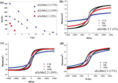
Figure 4. FC (squares) and ZFC (diamonds) for the sample aGeMn2.1. (b) Numerical derivative of the magnetization with respect to the temperature obtained with an applied field H = 50 Oe for aGeMn2.1. (c) Reciprocal values of the magnetic moment normalized to its value at Tmin = 2.5 K (1/MNorm) obtained with the same small applied field (H = 50 Oe) plotted vs. T.
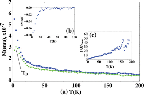
Figure 5. (a) FC (squares) and ZFC (diamonds) for the sample aGeMn2.3 and FC (triangles) and ZFC (inverted triangles) for the sample aGeMn2.2. (b) Numerical derivative of the normalized magnetization with respect to the temperature obtained with an applied field of H = 50 Oe for aGeMn2.2 (triangles) and aGeMn2.3 (squares). (c) reciprocal values of the normalized magnetization obtained with the same small applied field (H = 50 Oe) plotted vs. T. for aGeMn2.2 (triangles) and aGeMn2.3 (squares). (d) Fit of the experimental normalized magnetic moment for the sample aGeMn2.2 (triangles) and aGeMn2.3 (dots) obtained with Equation (Equation8(8)
(8) ).
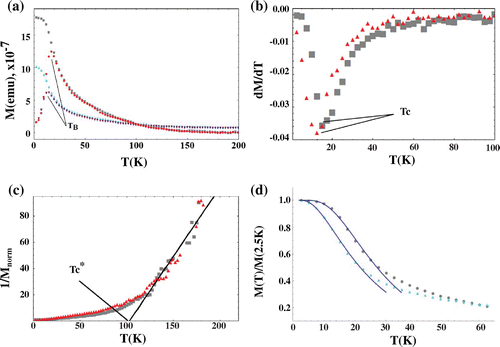
These indicate that a single smooth magnetic transition is present at low temperature in our samples. It has to be underline that the FC measurements have not display any TC around 300 K, ruling out also in this way the presence of fine crystalline precipitates. The concave shapes of the magnetization curves are in contrast with the convex Brillouin behaviour that is expected in a saturated ferromagnet according to the Weiss mean field theory.[Citation20] Conversely, these FC-ZFC curves closely resemble those that are routinely measured in superparamagnetic particles samples.[Citation21,22] In those systems, the appearance of a ferromagnetic behaviour below a blocking temperature TB is attributed to the presence of ferromagnetic particles (or precipitates in an otherwise non-magnetic matrix) having a much higher Curie temperature whose magnetization direction fluctuates in time because of the thermal agitation above TB, and remains ‘blocked’ along an anisotropy direction below this temperature. Indeed, it is possible to extract the values for the superparamagnetic blocking temperature (TB), occurring at the maximum of the ZFC curves for our samples: (aGeMn2.3 (17%)),
(aGeMn2.2 (10%)) and
(aGeMn2.1 (2%)). However, a pure superparamagnetic description of the behaviour of our aGe1-xMnx samples is somewhat misleading, as it would assume the presence of ferromagnetic precipitates that have not been observed in our case. Conversely, as we will see in the following, BMPs turn out to account for the measured magnetic properties in the whole temperature range, including below TB, where neither a superparamagnetic scaling law, nor a Stoner–Wohlfarth model can be invoked to describe the hysteresis loops reported in Figure .
In a system constituted by BMPs there are two characteristic temperatures at which the function M(T) (or its first derivative with respect to the temperature) presents a discontinuity [Citation23]: TC* and TC. The higher one (TC*) is the temperature at which the system undergoes the transition from a pure paramagnetic state to a superparamagnetic one. This temperature is identified (Figure (c)) as the one at which the susceptibility of the sample diverges from the linear behaviour and for crystalline Ge1-xMnx was found to be TC* = 112 ± 5 K for x = 0.05, and saturates as the percentage of Mn exceed the 5%.[Citation27] In the present case this temperature was found to be 103 ± 7 K for both the sample aGeMn2.2 (10%) and aGeMn2.3 (17%), a value compatible with previous result as expected; because this temperature, which is equivalent to the Mn-holes exchange coupling, should be independent from the crystalline structure if the carriers are localized. For the sample aGeMn2.1 the temperature at which the susceptibility starts to deviate from the linear behaviour could not be properly localized in (Figure (c)); this feature of the sample aGeMn2.1 can be accounted for the much lower Mn content of this sample.
At lower temperatures (TC < T < TC*), when BMPs start to stabilize, they possess a small radius and do not interact. In this condition they behave like a system of superparamagnetic nanoparticles. Indeed, above their blocking temperature the hysteresis loops are characterized by a zero value of the coercivity (Figure ), while a deviation from linearity of the M(H) function is clearly visible.
The feature which allows to distinguish this ensemble of uncorrelated BMPs from a system of magnetic nanoparticles is that their radius is temperature dependent [Citation12,27]:(7)
(7)
where is the spin of a Mn ion, s is the hole spin and J is the exchange integral between the holes and the impurities. A second temperature (TC) exists at which the isolated BMPs start to interact with each other through the impurities spatially located in between; this interaction can produce an alignment of the polaron spins, which can ‘aggregate’ into larger magnetic entities. These clusters will eventually percolate into an interconnected network when their radius becomes large enough at low temperature. In the low carrier density regime, in which the localization length is small compared to the mean distance between holes (σ ≡ a3nh < < 1), the shape of the
curve in the percolative regime can be expressed as [Citation16]:
(8)
(8)
where is the magnetic moment as T → 0. In the same framework, the Curie temperature (at which the percolative network is formed) is defined as:
(9)
(9)
where is the concentration of localized holes inside the semiconductor, M(T) and
are experimental values, while σ and J are fitting parameters.
For the samples aGeMn2.2 (10%) and aGeMn2.3 (17%) the value of M starts to saturate before reaching Tmin, giving rise to a plateau (Figure ). By plotting the value of dM/dT as a function of T (Figure (b)) it is possible to identify two characteristic temperatures for the samples aGeMn2.2 (10%) and aGeMn2.3 (17%) that are at and
respectively. By defining these two values as the Curie temperatures, we can fit the FC curves for T < TC by employing Equation (Equation8
(8)
(8) ). The two fits in Figure (d) display the good agreement between the experimental dependence and Equation (Equation8
(8)
(8) ), whereas this correspondence starts to vanish above TC. The values of σ and J as calculated through the fitting procedure are
,
for aGeMn2.3 (17%) and
,
for aGeMn2.2 (10%).
In case of the aGeMn2.1 (2%) sample, M monotonically increases till the lowest achievable temperature (); therefore, it is impossible to reach the minimum value of dM/dT (Figure (b)). In this case, no clear sign of ferromagnetic percolation is detectable, being the hysteretic behaviour of this sample at lower temperatures (Figure (b)) probably due to some residual degree of interaction between single polarons (
), which are randomly distributed inside the material. The sample aGeMn2.3 (17%) shows a paramagnetic response at higher T, related to the component
of the sum in Equation (Equation6
(6)
(6) ).
All the three samples exhibit a disordered magnetic ground state, as evidenced by the ZFC measurements (Figures and ). The interplay between the weak, antiferromagnetic, interaction that is present across nearby impurities (Mn atoms) and the long range coupling between the hole and the impurity spins in the intermediate region becomes comparable and can result in a spin disordered ground state. The BMPs still exist, but are surrounded by a large area of unpolarized impurities which, at very low temperature, freeze out into a spin glass state.
With the aid of Equation (Equation9(9)
(9) ), which provides the Curie temperature of percolated BMPs, and using the values of (
) from the previous fit, we can extract the localization length of the holes on the impurity levels introduced by the Mn atoms. Assuming the ratio nh/ni to be constant [Citation7] for the samples aGeMn2.3 (17%) and aGeMn2.2 (10%), we can rewrite the relationship for the Curie temperature with just one unknown parameter, that is,
:
(10)
(10)
Using this expression and the calculated value for σ and nie can therefore extract the value of the parameter, yielding:
(11)
(11)
and from this value of carrier compensation, we can extract the localization length as:
(12)
(12)
This value of LR is significantly smaller than the localization radius for the holes in crystalline lightly doped germanium () but is compatible with the radius evaluated with the same model in Mn-implanted germanium (
) [Citation7]. In addition with this value of LR at hand we can calculate by exploiting Equation Equation(5
(5)
(5) ) and the previously calculated values for T0, the densities of the states near the Fermi level which are
(aGeMn1.1) and
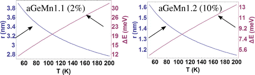
(aGeMn1.2). The mean hopping distances and energies are obtained for the other two samples by means of Equations (Equation2
(2)
(2) ) and (Equation3
(3)
(3) ) and the results are displayed in Figure . The mean hopping distance (r) should possess at least the same order of magnitude with respect to the average impurity distance also in the variable hopping range scenario: in the present case for the sample with Mn = 2% (10%) the average distance between impurities is 1 nm (0.6 nm). Taking into account the fact that roughly 30% of the impurity sites are occupied by the holes (
) and that, due to the complete spin polarization of the Mn 3D orbitals, in the demagnetized state only 50% of the sites are available for the hopping (due to the exclusion principle), the mean distances between available sites for Mn = 2% (10%) become 1.5 nm (0.9 nm). This value is comparable with the extracted values for the mean hopping distances which are r = 3.3 nm (1.4 nm) at 90 K.
Figure 6. Values of the mean hopping distance (r) expressed in nm and the mean activation energy (ΔE) expressed in meV for the samples aGeMn 1.1 (left panel) and aGeMn 1.2 (right panel) plotted vs. the temperature from Equations (2) and (3).
4. Conclusions
The electrical and magnetic properties of amorphous Ge1-xMnx thin films obtained through physical vapour co-deposition of Ge and Mn from solid sources have been studied by means of SQUID magnetometry and DC electrical measurements. It is shown that localization in such systems is the main physical mechanism that can account for both the electrical and magnetic properties, ruling out the presence of ferromagnetic precipitates that would have resulted in a composite system instead of a diluted magnetic semiconductor. The experimental results coming from the samples with higher atomic concentration of Mn (17% and 10%) can be unfolded using the bound magnetic polaron model, as it was possible to extract a Curie temperature for the magnetic percolation transition TC, and one for the polaron formation TC*. As in some of the crystalline counterparts [Citation7,23,24] the magnetic properties of these diluted amorphous alloys could be explained by the magnetic polaron model at low temperatures, but their coercive field at T < TC seems to be higher with respect to what was found in the crystalline counterpart; also the limit concentration below which it is possible to obtain the dilute system free of metallic precipitates is increased with respect to the crystalline material.[Citation23] The variable range hopping conduction mechanism and the strong carrier localization of this amorphous alloy does not substantially differ from what is observed in the crystalline diluted system (GaMnAs or GeMn),[Citation25,26] pointing out the strong role of the disorder induced by the random position of the manganese atoms in the host semiconductor matrix that is present in the crystalline DMSs as well.
Disclosure statement
No potential conflict of interest was reported by the authors.
Acknowledgments
The authors would like to thank Dr Elena Olivetti for the XRD measurements and Dr Alfio Battiato for the XPS measurements.
References
- Park YD, Hanbicki AT, Erwin SC, et al. A Group-IV ferromagnetic semiconductor: MnxGe1-x. Science. 2002;295:651–654.10.1126/science.1066348
- Jamet M, Barski A, Devillers T, et al. High-Curie-temperature ferromagnetism in self-organized Ge1− xMnx nanocolumns. Nat Mater. 2006;5:653–659.10.1038/nmat1686
- Ottaviano L, Continenza A, Profeta G, et al. Room-temperature ferromagnetism in Mn-implanted amorphous Ge. Phys Rev B. 2011;83:134426.10.1103/PhysRevB.83.134426
- Yada S, Sugahara S, Tanaka M. Magneto-optical and magnetotransport properties of amorphous ferromagnetic semiconductor Ge1−xMnx thin films. Appl Phys Lett. 2008;93:193108.10.1063/1.3023070
- Li H, Wu Y, Guo Z, et al. Magnetic and electrical transport properties of Ge1−xMnx thin films. J Appl Phys. 2006;100:103908.10.1063/1.2375015
- Yu SS, Anh TTL, Ihm YE, et al. Magneto-transport properties of amorphous Ge1−xMnx thin films. Curr Appl Phys. 2006;6:545–548.10.1016/j.cap.2005.11.057
- Morgunov RB, Dmitriev AI, Kazakova OL. Percolation ferromagnetism and spin waves in Ge: Mn thin films. Phys Rev. 2009;80:085205.10.1103/PhysRevB.80.085205
- Xiu F. Magnetic Mn-doped Ge nanostructures. ISRN condens matter phys. 2012;2012:198590.
- Chien CL, Liou S-H, Kofalt D, et al. Magnetic properties of FexCu100− x solid solutions. Phy Rev B. 1986;33:3247.10.1103/PhysRevB.33.3247
- Ahmed N, Hicks TJ. Magnetic and atomic correlations in dilute copper-manganese alloys. J Phys F: Met Phys. 1975;5:2168.10.1088/0305-4608/5/11/028
- Bhatt RN, Berciu M, Kennett MP, et al. Diluted magnetic semiconductors in the low carrier density regime. J supercon. 2002;15:71–83.10.1023/A:1014031327996
- Kaminski A, Das Sarma S. Polaron percolation in diluted magnetic semiconductors. Phys Rev Lett. 2002;88:247202.10.1103/PhysRevLett.88.247202
- Bednarski H, Jozef S. Bound-magnetic-polaron molecule in diluted magnetic semiconductors. J Phys: Condens Matter. 2012;24:235801.
- Massenet O, Daver H, Geneste J. Magnetic ordering and magnetization in amorphous Fe-Ge films. J Phys Colloq. 1974;35:C4–279.
- Mott NF, Davis EA. Electronic processes in non-crystalline materials. Oxford: OUP; 2012.
- Korenblit IYa, Shender EF. Ferromagnetism of disordered systems. Sov Phys Usp. 1978;21:832.10.1070/PU1978v021n10ABEH005686
- Cultrera A, Amato G, Boarino L, et al. A modified cryostat for photo-electrical characterization of porous materials in controlled atmosphere at very low gas dosage. AIP Adv. 2014;4:087134.10.1063/1.4894074
- Shklovskii BI, Efros AL. Electronic properties of doped semiconductors. New York, NY: Springer-Verlag Inc; 1984.10.1007/978-3-662-02403-4
- Mott NF. Conduction in non-crystalline materials: III. localized states in a pseudogap and near extremities of conduction and valence bands. Phil Mag. 1969;19:835–852.10.1080/14786436908216338
- Cullity BD, Graham CD. Introduction to magnetic materials. Piscataway (NJ): John Wiley; 2011.
- Hansen MF, Mørup S. Estimation of blocking temperatures from ZFC/FC curves. J Magn Magn Mater. 1999;203:214–216.10.1016/S0304-8853(99)00238-3
- Bean CP, Livingston JD. Superparamagnetism. J Appl Phys. 1959;30:S120–S129.10.1063/1.2185850
- Li A-P, Wendelken JF, Shen J, et al. Magnetism in MnxGe1− x semiconductors mediated by impurity band carriers. Phy Rev B. 2005;72:19520510.1103/PhysRevB.72.195205
- Kumar S, Paschoal W Jr, Johannes A, et al. Magnetic polarons and large negative magnetoresistance in GaAs nanowires implanted with Mn ions. Nano Lett. 2013;13:5079–5084.10.1021/nl402229r
- Paschoal W Jr, Kumar S, Borschel C, et al. Hopping conduction in Mn ion-implanted GaAs nanowires. Nano Lett. 2012;12:4838–4842.10.1021/nl302318f
- Pinto N, Morresi L, Ficcadenti M, et al. Magnetic and electronic transport percolation in epitaxial Ge1–xMnx films. Phy Rev B. 2005;72:165203.10.1103/PhysRevB.72.165203
- Das Sarma S, Hwang EH, Kaminski A. Temperature-dependent magnetization in diluted magnetic semiconductors. Phy Rev B. 2003;67:155201.10.1103/PhysRevB.67.155201