
 ?Mathematical formulae have been encoded as MathML and are displayed in this HTML version using MathJax in order to improve their display. Uncheck the box to turn MathJax off. This feature requires Javascript. Click on a formula to zoom.
Abstract
Photoelectrochemical water-splitting is a promising carbon-free fuel production method for producing H2 and O2 gas from liquid water. These cells are typically composed of at least one semiconductor photoelectrode which is prone to degradation and/or oxidation. Various surface modifications are known for stabilizing semiconductor photoelectrodes, yet stabilization techniques are often accompanied by a decrease in photoelectrode performance. However, the impact of surface modification on charge transport and its consequence on performance is still lacking, creating a roadblock for further improvements. In this review, we discuss how density functional theory and finite-element device simulations are reliable tools for providing insight into charge transport across modified photoelectrodes.
1. Introduction
Photovoltaic and photoelectrochemical (PEC) cells are two devices capable of harvesting the solar power incident on Earth by converting sunlight into electric power and/or chemical fuels [Citation1]. High conversion efficiencies recently observed in PEC cells have motivated research to move from conventional photovoltaics towards a new generation of PEC cells [Citation2,Citation3]. These cells utilize a semiconductor photoelectrode to capture and convert incident light into free charge carriers that are exploited to provide the electrochemical difference required to generate chemical fuels. A promising carbon-free fuel-production method is PEC solar-driven water-splitting where hydrogen (H2) and oxygen (O2) gas are generated from liquid water [Citation4–15].
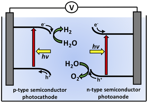
A 1.23 V electrochemical difference is required as a minimum to drive PEC water-splitting, which can only be provided by a single semiconductor with an excessively large band-gap. An alternative strategy is to use two small band-gap semiconductors placed electrically in series. One semiconductor operates as the photocathode to drive H2-evolution while the other operates as the photoanode to drive O2-evolution, as shown in Figure . In this case, the electrochemical potential difference required to split water is partially provided by each semiconductor. However, small band-gap semiconductors typically dissolve or develop insulating oxide coatings during PEC operation. Current research is focused on developing various techniques for stabilizing small band-gap semiconductors for use in a technologically viable, efficient, and stable solar-driven water-splitting system.
Figure 1. Schematic of a two-electrode photoelectrochemical water-splitting cell where a p-type semiconductor operates as the photocathode to evolve hydrogen while an n-type semiconductor operates as a photoanode to evolve oxygen.
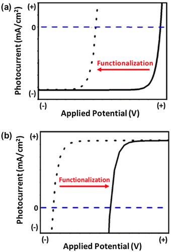
Surface modification is commonly used in PEC cells [Citation31,Citation32] as well as a variety of additional applications such as electronic devices [Citation16–21], data storage [Citation22], chemical sensing [Citation23–25], molecular nanopatterning [Citation26], and bioengineering [Citation27–30]. In PEC applications, chemical attachment of organic molecules is a versatile technique used to enhance the stability of low-gap semiconductors while controlling the physiochemical properties of the surface [Citation33]. For example, Lewis et al. have shown that forming covalent Si-C bonds on the surface of Si(111) photoelectrodes prevents oxidation of the surface [Citation34]. Alternatively, depositing a thin layer of metal oxide such as SiO2 [Citation35], Al2O3 [Citation36,37], TiO2 [Citation38–42], or ZnO [Citation43] has been shown to passivate a variety of semiconductor surfaces. Although functionalizing a semiconductor with organic molecules or passivation layers stabilizes the surface, the modification often results in a less preferable onset potential of the semiconductor photoelectrode as shown for a p-type photocathode (more negative) and n-type photoanode (more positive) in Figure (a) and Figure (b), respectively.
Figure 2. Commonly observed impact of surface functionalization on the photocurrent versus voltage response of a (a) p-type semiconductor photocathode and (b) n-type semiconductor photoanode.
An understanding of how surface modification influences charge transport and reduces the onset potential of a functionalized semiconductor photoelectrode is still lacking. This creates a roadblock for further improvements in device performance and a lack of design rules for identifying candidate materials for functionalization. In this review, we discuss how computational modeling can be used to provide insight into charge transfer across heterojunction structures. Specifically, we show examples of applying first-principles density functional theory and finite-element device simulations to investigate the effects of organic functionalization and passivating layers on charge transport across an underlying semiconductor surface.
2. Experimental methods
2.1. Photocurrent versus voltage response
Photoelectrode performance can be quantified experimentally by measuring the photocurrent density versus voltage (J-V) response for a specified potential range under solar illumination in contact with a redox couple. Two benchmarks directly related to the performance are obtained from the J-V curve: (1) short-circuit current density (Jsc), which is the maximum observed current at 0 V applied potential and (2) onset potential for the redox reaction (Von,A), which is the voltage at which the net current across the device is zero.
The onset potential is a key metric of performance for photoelectrochemical devices because it is related to the open-circuit photovoltage, Voc, which is the maximum energy that can be obtained from the collection of photons to drive electrical current and/or a chemical reaction. The Voc can be calculated from Von,A using [Citation44](1)
(1)
where E(A/A-) is the formal redox potential of the redox couple in contact with the photoelectrode. The maximum Voc that can be achieved for a device is limited by recombination processes in the bulk of the material and can calculated for a p-type semiconductor as [Citation45](2)
(2)
where Jph is the photocurrent density, Ln is the minority carrier diffusion length, Dn the minority carrier diffusion coefficient, Nc the effective density of states in the conduction band, and Vp the difference in energy between the Fermi and valence band energies in the bulk. A similar equation can be written for an n-type semiconductor. A Voc less than the value calculated by Equation (Equation2(2)
(2) ) is a consequence of deleterious surface or bulk effects in the semiconductor such as poor diffusion lengths, thermionic emission or tunneling across heterojunctions or surface barriers, transport through chemical imperfections, surface/bulk state recombination, or Fermi level pinning [Citation45, Citation46].
2.2. Dipole measurements
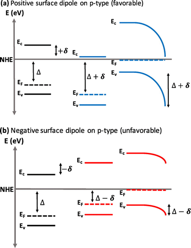
Functionalization of a photoelectrode with organic molecules has been observed to dramatically affect the Voc due to a change in the magnitude and direction of the surface dipole induced by the organic molecule. For a p-type semiconductor, a molecule that induces a large positive dipole (negative charge on the molecule, positive charge on the substrate) increases the Voc by increasing the barrier height and depletion width at the surface as shown in Figure (a), while a negative dipole (positive charge on the molecule, negative charge on the substrate) decreases the barrier height and depletion width as shown in Figure (b). For an n-type semiconductor the behavior is reversed and a molecule with a negative dipole increases the Voc by increasing the barrier height and depletion width at the surface.
Figure 3. The effect of a (a) positive (favorable) and (b) negative (unfavorable) surface dipole on the band bending and depletion width of a p-type semiconductor.
The surface dipole (δ) is defined as the difference between the electron affinity at the surface (χs) and the electron affinity in the bulk (χB) of the semiconductor(3)
(3)
χs can be expressed in terms of the work function at the surface (Φs), band gap of the semiconductor (Eg), and the absolute energy difference between the valence band edge and the Fermi level (|Ev−EF|s) at the surface resulting in an expression for the surface dipole as
(4)
(4)
Equation (Equation4(4)
(4) ) allows for a direct determination of the surface dipole because the values of Eg and χB can be found in literature while the magnitude of
and |Ev−EF|s can be measured from ultraviolet photoelectron spectroscopy (UPS) and X-ray photoelectron spectroscopy data (XPS), respectively [Citation47–49].
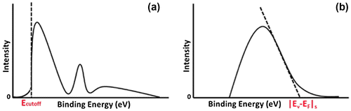
The work function of a semiconductor can be determined using UPS via the following expression(5)
(5)
where hv is the excitation energy (typically He I emission at 21.2 eV) and Ecutoff is the secondary electron cutoff energy in the photoelectron spectra [Citation50]. The secondary emission is due to secondary electrons, which are defined as those that have lost energy due to inelastic collisions when traveling to the sample surface. The secondary emission is characterized by a broad, continuous peak. Ecutoff is determined graphically by extrapolating the secondary electron cutoff energy to the background intensity as shown in Figure (a). |EV−EF|s can be determined using XPS with He II emission at 40.82 eV. The value of |EV−EF|s is determined graphically by extrapolating the steep emission onset in the spectra to zero signal as shown in Figure (b). Once and |EV−EF|s are determined the sign and magnitude of the surface dipole can be calculated using Equation (Equation4
(4)
(4) ).
Figure 4. (a) Schematic of ultraviolet photoelectron emission data with the value of the cutoff energy indicated on the plot. (b) Schematic of X-ray photoelectron spectroscopy data with the value of the absolute energy difference between the valence band-edge and the Fermi level (|EV- EF|s) at the surface indicated on the plot.
3. Theoretical methods
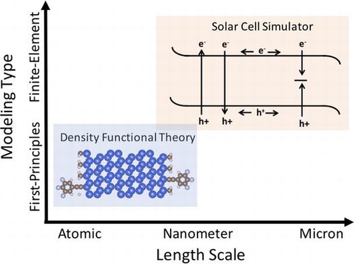
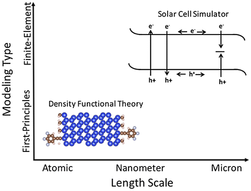
We demonstrate simulation-based improvement of charge transport across modified semiconductor surfaces by utilizing two independent computational methods: first-principles density functional theory [Citation51,52] and a finite element-based device simulator known as wxAMPS [Citation53]. Density functional theory is utilized to investigate the electronic properties of the semiconductor surface at the atomic level while wxAMPS provides insight into the performance of the semiconductor photoelectrode at the device level. Utilizing both computational methods provides a theoretical tool for analyzing the system from the atomic to the device level as shown in Figure .
Figure 5. Schematic of the two computational methods described in this review. First-principles modeling is on the scale of electrons/atoms while device simulations are on the micron/device scale.
3.1. Density functional theory
Density functional theory (DFT) is a quantum mechanical modeling method applicable to atomic scale systems and widely employed in the field of computational chemistry and physics. DFT is used to investigate the electronic structure of many-body systems by solving the Schrödinger equation to yield the total energy (E) of a system(6)
(6)
where H is the Hamiltonian operator and ψ is the wavefunction depending on the spatial coordinates of electrons, , and nuclei,
, in the system.
Equation (Equation6(6)
(6) ) represents a many-body system with N electrons and 3 N total spatial coordinates, which is computationally intractable. Therefore, an approximation known as Kohn-Sham DFT is often used in which the system is approximated as a collection of non-interacting electrons moving in an effective potential, Veff. Equation (Equation6
(6)
(6) ) then becomes a one-electron Schrödinger equation for a 3-coordinate system described by Equation (Equation7
(7)
(7) )
(7)
(7)
where εi is the energy eigenvalue corresponding to the Kohn-Sham one-electron wavefunction, . The charge density,
, for the N-electron system is obtained as a sum over occupied states by Equation (Equation8
(8)
(8) )
(8)
(8)
The use of Kohn-Sham DFT requires an approximate exchange-correlation functional chosen to represent the spatial dependence of the effective potential. The accuracy of DFT in modeling various systems is limited by the chosen functional for the system. However, because DFT is often used to calculate the energy difference between various systems, errors due to the exchange-correlation functional often cancel leading to reliable results.
The most commonly chosen functionals are LDA [Citation54] and PBE [Citation55] due to their computational reliability and low computational cost. Nowadays, more sophisticated options are available such as hybrid functionals, however, these are often still computationally limiting. Many codes are available to compute DFT calculations including VASP [Citation56–60], Quantum Espresso [Citation61], and SIESTA [Citation62].
3.1.1. Modeling surfaces
First-principles calculations based on DFT have become a powerful tool for calculating surface properties of semiconductors [Citation63–72]. Surface calculations using DFT are often computed using a planewave basis [Citation73] and a slab configuration (see Figure ). The slab is placed within a 3D periodic super-cell and a vacuum layer is added on either side of the slab to mimic the 2D periodicity of an actual surface. The number of slab layers should be thick enough to minimize surface-surface interactions and recover a bulk-like interior. Similarly, the vacuum layer is thick enough such that interactions between the two sides of the slab or the formation of a net dipole are avoided.
Figure 6. (a) Asymmetric slab configuration where the top side of the slab is terminated with a mixed monolayer of trifluorophenylacetylenyl and methyl groups while the bottom side is passivated with hydrogen. (b) Symmetric slab configuration where the top and bottom sides of the slab are terminated with a mixed monolayer of trifluorophenylacetylenyl and methyl groups. In both configurations 12 Å of vacuum separates the surfaces of the slab. The dark blue, brown, light pink, and light blue atoms represent silicon, carbon, hydrogen, and fluorine, respectively.
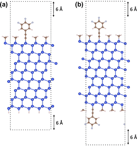
A slab may have an asymmetric (Figure (a)) or symmetric (Figure (b)) configuration which are defined as having different or identical terminations on the two sides of the slab, respectively. When using an asymmetric slab, an artificial electric field is automatically added to the cell to eliminate the potential step resulting from a difference in the two sides of the slab. This field may artificially change the electronic structure of the absorbed monolayer resulting in qualitative as well as quantitative errors.
An established method to correct for the artificial electric field is to place a dipolar sheet inside the vacuum region such that the total dipole across the super cell is zero [Citation74]. However, we and others have found that this correction scheme often results in convergence problems [Citation70]. To avoid the convergence issues associated with calculating the total dipole for an asymmetric slab, we recommend using a symmetric slab when possible because the total dipole for a symmetric slab is zero, which eliminates the artificial electric field. In some situations, it is necessary to use an asymmetric slab, such as for polar/non-centrosymmetric crystals with opposite terminations. In this case, a very large vacuum region may be used (30+ Å) to mitigate the magnitude of the electric field interacting with the surface but convergence of properties with respect to vacuum length is slow.
3.1.2. Quantifying a surface dipole
The interfacial dipole of a semiconductor functionalized with an arbitrary functional group can be calculated using DFT by a procedure known as nanosmoothing developed by Rabe et al. [Citation75]. Nanosmoothing is used to eliminate bulk effects and extract well-defined, unique values of the interfacial charge and dipole densities for a system. The procedure involves calculating a smoothed charge density, , in which periodic bulk oscillations in the microscopic charge density are removed by convoluting the planar-averaged charge density calculated in Equation (Equation9
(9)
(9) ) with a smoothing function f(z) as shown in Equation (Equation10
(10)
(10) ) [Citation74, Citation76]
(9)
(9)
(10)
(10)
where A is the surface area of the slab in the z-direction. The planar-average charge density and the nanosmoothed charge density are shown in Figure (a) and (b), respectively, for the symmetric terminated Si(111) slab configuration shown in Figure (b).
Figure 7. Planar average charge density and nanosmoothed average charge density for the symmetric terminated Si(111) slab configuration shown in Figure 6(b).
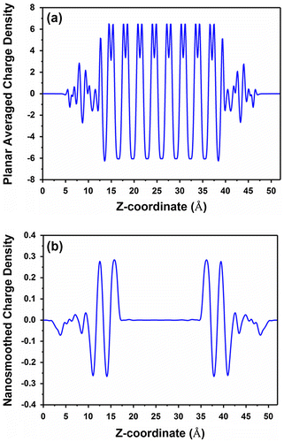
The smoothed charge density is a continuous function that approaches zero at regions far from the interface. The interface is defined as the region where the smoothed charge density deviates away from zero. The nanosmoothed dipole density, , is unique and well defined if z1 and z2 are in regions where the smoothed charge density is zero and is calculated using
(11)
(11)
3.2. Finite-element device simulations
wxAMPS is a drift-diffusion solid-state device simulation application based on AMPS, a solar cell simulation program developed by Fonash et al. at Pennsylvania State University [Citation77]. wxAMPS has the same user inputs and physical principles as AMPS but incorporates a more advanced algorithm combining the Newton and Gummel methods [Citation78] to facilitate convergence and improved models of recombination and tunneling [Citation79,80]. wxAMPs is available free of charge on the web and has an easy-to-use graphical user interface [Citation81]. wxAMPS has been demonstrated to model a variety of complex devices including dye-sensitized solar cells [Citation82] and functionalized photoelectrodes [Citation83,84].
wxAMPS simulates charge generation, recombination, and transport across single or multijunction devices by solving Poisson’s equation, the continuity equation for free holes, and the continuity equation for free electrons simultaneously. wxAMPS uses the one-dimensional form of Poisson’s equation to relate the charge carrier concentrations throughout the device to the electrostatic potential, V, referenced to the position of the local vacuum level:(12)
(12)
where n, p, nt, pt, ND+, NA- are the free electron, free hole, trapped electron, trapped hole, ionized donor, and ionized acceptor state concentrations as a function of position x in the device. ɛ is the permittivity of the material and q is the magnitude of the charge of an electron. The continuity equations for free electrons and holes in the delocalized states of the conduction band and valence band are given by Equations (Equation13(13)
(13) ) and (Equation14
(14)
(14) )
(13)
(13)
(14)
(14)
where Jn and Jp are the electron and hole current densities, respectively. R(x) is the net recombination rate from band-to-band and/or via Shockley-Read-Hall recombination, while Gop(x) is the optical generation rate from illumination. A more detailed description of the model and the implementation of boundary conditions is described in previous work [Citation83].
4. Application of computational methods
4.1. Organic functionalization
Chemical attachment of organic molecules to a semiconductor surface may alter the direction and magnitude of the dipole at the surface [Citation32]. We describe here how density functional theory and wxAMPS can be combined to quantify the dipole of an arbitrary functionalization and the methods are then compared with experimental measurements.
4.1.1. Band-edge control of silicon
Galli et al. conducted a combined theoretical and experimental study on the band-edge control of functionalized silicon [Citation71]. Theoretical methods included electronic structure calculations using DFT and many-body perturbation theory (MBPT), while experimental methods included photoelectron spectroscopy and electrical device measurements. In their work, the ionization potential (IP), defined as the energy of the maximum valence band-edge relative to vacuum, of -H, -CH3, -C2H5, -Cl, and -Br terminated Si(111) surfaces were compared.
The IPs were determined experimentally by measuring the work function using ultraviolet photoelectron spectroscopy and calculating the IPs from(15)
(15)
where Evb and Evs are the bulk and surface valence-band levels, respectively. Ecb – EF is calculated from the dopant density and Ebb is derived via a methodology described in Ref [Citation48]. The IPs were calculated using DFT with local density approximation (LDA) exchange potentials and MBPT with the perturbative G0W0 approach.
At the LDA level, the calculated IPs were underestimated by 0.5–0.7 eV compared to the experimental results, while the values improved significantly using G0W0. However, the relative shifts in the IP between a given functionalization and Si(111)-H, ΔIPR:H, were the same for both LDA and GW and also in satisfactory agreement with experiments. Therefore, they suggested that LDA is adequate for predicting the absolute value for IP, IPpred, without resorting to expensive GW calculations. This is done by calculating the shift between a given functionalization and a well-defined reference state, , and using
(16)
(16)
where is the experimental known value of the IP for the reference state used to calculate
.
Shifts in the IP are a consequence of a shift in the surface potential, ΔVsurf, which is related to the formation of a surface dipole normal to the surface plane of the unit cell, , by
(17)
(17)
μsurf,z can be quantified as the sum of the dipole moment formed in the adsorbate radical, and the induced dipole moment due to charge transfer between the substrate and the absorbed molecule,
. To gain an understanding of how the magnitude of
depends on the composition and coverage of the adsorbate, Galli et al. computed
and
for a variety of terminal groups at both one-quarter and full coverage [Citation71]. μind,z was calculated using
=
. They found that for non-polar terminal groups,
, trends in electronegativity dictated the charge exchange at the adsorbate/substrate interface and hence could be used to predict the magnitude of
. They found that for polar terminal groups the magnitude of
depends on the orientation and surface coverage of the adsorbate, strength of intermolecular screening, and molecular polarizability.
In another study, the composition and coverage of mixed monolayers on Si(111) was found to have a significant effect on the interfacial dipole. The dipole as a function of coverage of 3,4,5-trifluorophenylacetylenyl (TFPA) moieties on Si(111) for both mixed methyl/TFPA and mixed chlorine/TFPA terminated surfaces was calculated using the nanosmoothing method discussed in section 3.1.2 [Citation85]. The method was validated and the calculated trends were consistent with previously published experimental data. Significant interactions were found between neighboring species on the functionalized surface that significantly altered the magnitude of the interfacial dipole as shown in Figure . These results imply that the chemical species passivating non-bonded sites (i.e. -H, -Cl, -CH3, etc.) must match the experimental surface when predicting surface dipoles using DFT. These findings also suggest that the effective band-edge energies of a surface can be engineered to have a specific value by tuning the interfacial dipole with the chemical make-up of a mixed monolayer.
Figure 8. Lateral interactions are observed between neighboring moieties on mixed monolayers of Si(111) functionalization with trifluorophenylacetylene (TFPA) and -CH3/Cl. Reprinted with permission from J. Phys. Chem. C, 121, 11312–11318. Copyright 2017 American Chemical Society [Citation85].
![Figure 8. Lateral interactions are observed between neighboring moieties on mixed monolayers of Si(111) functionalization with trifluorophenylacetylene (TFPA) and -CH3/Cl. Reprinted with permission from J. Phys. Chem. C, 121, 11312–11318. Copyright 2017 American Chemical Society [Citation85].](/cms/asset/bf474a15-fb8c-45bc-b580-90dac1162cfa/tsta_a_1370962_f0008_oc.gif)
wxAMPS can also be used to predict the magnitude of an interfacial dipole on a functionalized semiconductor by fitting experimental data [Citation83]. For example, Lewis et al. previously measured the Voc for n and p-type Si(111)-H and Si(111)-CH3 photoelectrodes in contact with a series of redox couples in CH3CN-1.0 M LiClO4 [Citation33]. Two different behaviors were observed for Si(111)-H and Si(111)-CH3. The magnitude of the surface dipole was predicted using wxAMPS by fitting the experimental trends. Because an interfacial dipole modifies the effective electron affinity of the surface of the semiconductor, the magnitude of the electron affinity was adjusted until the calculated trend in Voc versus redox formal potential matched the experimental data. The results predicted a dipole shift of −0.35 eV between Si(111)-H and Si(111)-CH3 [Citation83].
The dipole shift between Si(111)-H and Si(111)-CH3 was calculated in Galli’s work with DFT and many-body perturbation theory (MBPT) and found to be −0.8 eV in contact with vacuum [Citation71]. The dipole shift determined using impedance spectroscopy in contact with octamethylferrocene-CH3CN-1.0 M LiClO4 is measured as −0.4 V and −0.25 V for n and p-Si(111), respectively [Citation33]. The dipole shift determined using photoelectron spectroscopy in contact with vacuum is measured as −0.49 eV [Citation48,49], [Citation86,87]. These results are summarized in Table below.
Table 1. Comparison of experimental and theoretical reports of the dipole shift between Si(111)-CH3 and Si(111)-H.
As can be seen in Table the dipole shift determined from wxAMPS is in better agreement with the experimental values than DFT and MBPT. In experiment, partial screening of a surface dipole occurs in the presence of an electrolyte. This effect is captured by wxAMPS because the value is determined by fitting experimental data directly. The resulting value includes both the raw dipole and the screening effects to yield the true final dipole of the complete system. The presence of the electrolyte is ignored when predicting the dipole using DFT and MBPT since the surface is simulated in contact with vacuum. Therefore, the difference between the values of the dipole determined by wxAMPS and DFT/MBPT provides insight into the degree of electrolyte screening occurring in a system (−0.45 eV in the example above). We note that the screening effect reduces the dipole by a factor of two or more. However, we have found that DFT is reliable for computing relative values of interfacial dipole.
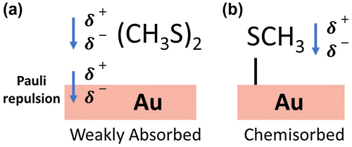
4.1.2. Organic-metal interfaces
Pennino et al. conducted a combined theoretical and experimental study on the work-function changes of metals functionalized by organic adsorbates [Citation88]. Comparison between experiment and theory provided a clear picture of the role of molecular dipole moment, charge transfer, and Pauli repulsion on the work-function changes induced by functionalization. Theoretical methods included electronic structure calculations using DFT while experimental methods included photoelectron spectroscopy. The work-function changes of dimethyldisulfide, (CH3S)2 (DMDS), and methylthiolate, CH3S (MT) terminated Au(111) were compared. The work function changes were determined experimentally using UPS and theoretically by calculating the difference between the electrostatic potential in vacuum, Vvacuum, and the Fermi level of the Au(111), EFermi:(18)
(18)
The experimentally observed work-function changes for DMDS and MT terminated Au(111) were found to be −1.2 and −1.5 to −1.7 eV, respectively, relative to the clean Au(111) surface, which is in good agreement with the calculated values of −1.2 and −1.6 eV, respectively.
To determine the main mechanism for the observed work-function shift the electrostatic potential for the total system, Vtotal, was compared with the sum of the electrostatic potential of the two subsystems, Vsubsystems, which consisted of the Au surface slab and molecular layer. For MT terminated Au(111), Vtotal − Vsubsystems remains constant across the interface implying no charge transfer and that the dominant mechanism responsible for the work-function shift is the molecular dipole moment intrinsic to MT. This was confirmed by the good agreement between the calculated molecular dipole of the isolated MT layer and the experimental observation. For DMDS-terminated Au(111), Vtotal − Vsubsystems decreases across the interface implying a transfer of electrons from the adsorbate layer to the Au substrate. Because the electron affinity between DMDS is the same as Au, the charge displacement must arise from compression of the Au surface charge density into the Au bulk due to Pauli repulsion with electrons in the DMDS layer. This comparison is illustrated in Figure .
Figure 9. Comparison of (a) weakly absorbed DMDS on Au in which the main contributions to the work-function shift are the dipole intrinsic to the molecule and charge displacement via Pauli repulsion and (b) MT on Au in which the only contribution to the work-function shift is the dipole intrinsic to the molecule.
4.2. Passivation layers
Coating a photoelectrode with a thin film metal oxide passivation layer is commonly employed to protect semiconductor surfaces against oxidation. However, metal oxide passivation layers may increase or decrease the onset potential of the electrode depending on the deposition conditions of the metal oxide and thus how charge is transferred across the heterostructure [Citation42]. Javey et al. have observed that the photovoltage of p-InP photoelectrodes, which were passivated with TiO2 grown by atomic layer deposition (ALD), strongly depends on the type of titanium precursor used to grow the film. They found that in one case the TiO2 was ‘leaky’ and allowed significant hole conduction across the film resulting in a lower photovoltage. In an alternative case, the TiO2 was ‘non-leaky’ and hole conduction was blocked, resulting in a higher photovoltage [Citation42].
We describe here how the link between the charge transport behavior and the magnitude and direction of the induced shift in open-circuit potential can be understood by using wxAMPS to model the generation, recombination, and charge transport across semiconductor/metal-oxide heterostructures.
4.2.1. Leaky amorphous titanium dioxide
In semiconductor/metal-oxide heterostructures, a large valence band offset is usually observed between the wide-gap metal oxide and a relatively low-gap underlying semiconductor, which results in a barrier to hole transport across the photoelectrode. However, recent studies of amorphous TiO2 (‘a-TiO2’) grown by ALD using a nitrogen-based precursor resulted in a new ‘leaky dielectric’ passivation layer in which sufficient hole transport is observed through films hundreds of nanometers thick [Citation89, Citation90]. The hole charge transport mechanism responsible for this leakage current is poorly understood experimentally due to the lack of methods available for probing such transport.
wxAMPS has been used to investigate the ‘leaky’ dielectric transport mechanism. Rose et al. measured the anodic photocurrent of n-Si(111)-CH3|a-TiO2 electrodes as a function of a-TiO2 thickness [Citation39]. They found that a maximum hole current was observed for sufficiently thin a-TiO2, decreasing beyond a critical thickness and resulting in negligible current as shown in Figure (a).
Figure 10. (a) Current versus TiO2 thickness behavior observed experimentally, (b) the two transport mechanisms simulated in wxAMPS: red arrow (tunneling), blue arrow (defect mediated transport), and (c) simulated current versus thickness behavior for the tunneling (red dashed) and defect-mediated transport (blue solid). Reprinted with permission from J. Phys. Chem. C., 120 (45), 25697–25708, 2016. Copyright 2016 American Chemical Society [Citation39].
![Figure 10. (a) Current versus TiO2 thickness behavior observed experimentally, (b) the two transport mechanisms simulated in wxAMPS: red arrow (tunneling), blue arrow (defect mediated transport), and (c) simulated current versus thickness behavior for the tunneling (red dashed) and defect-mediated transport (blue solid). Reprinted with permission from J. Phys. Chem. C., 120 (45), 25697–25708, 2016. Copyright 2016 American Chemical Society [Citation39].](/cms/asset/a2e37994-d7e4-4649-a0b2-e64d59c9fe03/tsta_a_1370962_f0010_oc.gif)
Two different hole conduction mechanism have been suggested for this observed behavior: tunneling and defect mediated transport. Both transport mechanisms were simulated in wxAMPS for n-Si(111)|CH3|a-TiO2 photoelectrodes. The tunneling simulation results in an immediate, exponentially decreasing current versus TiO2 thickness which did not match the experimental observation. The defect mediated transport mechanism shown in Figure (b), where holes move through a defect band in the band gap of the TiO2, was shown by wxAMPS to match the experimentally observed photocurrent versus thickness response.
4.2.2. Non-leaky amorphous titanium dioxide
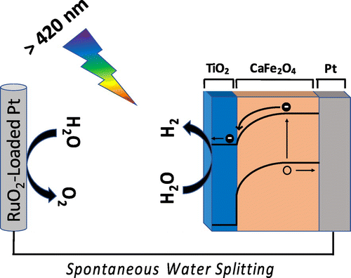
CaFe2O4 (CFO) is a promising p-type semiconductor to serve as a photocathode for H2-evolution in a PEC water-splitting system [Citation91,92]. TiO2 has been introduced as a passivation layer on CFO and shown to improve the chemical stability of the material [Citation84]. Despite improved stability, the onset potential of the photocathode upon TiO2 deposition is reduced. wxAMPS was used to determine the charge transport limitation behind the reduced onset potential and predict ways to improve the TiO2-coated CFO photocathode [Citation84].
Modeling both the coated and uncoated CFO photocathode behaviors showed that the reduction in onset potential upon coating CFO with TiO2 was a consequence of photo-generated charge trapping in the TiO2. When the CFO/TiO2 photocathode is under irradiation from a full spectrum solar simulator, the wavelengths of light that exceed the band-gap of TiO2 result in photoexcitation of carriers within the TiO2 layer. These accumulate in surface trap states, resulting in an electric field in the TiO2 that reduces the Voc. The simulations predicted that the reduction in the onset potential could be avoided by utilizing a UV light filter and only exciting the CFO/TiO2 photocathode with visible light. Excluding the UV light, the TiO2 acts as a protective electron-selective contact between the CFO and the electrolyte and the trap states in the TiO2 do not influence the onset potential. The simulation results predicted an onset potential of ~1.9 V versus a reversible hydrogen electrode (RHE). This indicated that the Voc of TiO2-coated CFO under longer wavelength irradiation should provide enough electrochemical potential to evolve H2 in a PEC water-splitting cell without an external applied voltage.
The simulation predictions were validated experimentally. First, the onset potential of the CFO/TiO2 photocathode under visible light irradiation was measured and found to be at minimum 1.6 V versus RHE. The actual onset potential could not be observed due to the onset of water electrolysis allowing current flow. The optimized TiO2-coated CFO under visible light irradiation had the most positive onset potential among the oxide photocathodes ever reported for PEC water-splitting, which was achieved by understanding the charge transport using wxAMPS. The TiO2-coated CFO photocathode was connected in series with a RuO2-loaded Pt system and under 470 nm excitation (visible light), evolution of H2 without an external applied bias was observed. A schematic of the device including the charge transport mechanism within the CFO/TiO2 photocathode is shown in Figure .
Figure 11. Schematic of a photoelectrochemical cell consisting of TiO2-coated/CaFe2O4 in series with RuO2-Loaded Pt. This cell split water spontaneously without an applied bias under visible light illumination. The cell was designed and optimized using wxAMPS simulations.
5. Future directions
Throughout this review, we have shown that density functional theory and finite-element device modeling are capable of providing insight into the charge transport characteristics of complex heterojunctions. Both models have been used to investigate charge transfer across heterojunctions consisting of metals, semiconductors, dielectrics, and electrolytes, including surfaces chemically functionalized with organic moieties. Predictions made using these computational tools have been demonstrated to be correct through subsequent experiments. The methods described can thus be used to significantly improve the performance of photoelectrochemical devices.
To further improve the predictive potential of the models, the two levels of theory must be connected as a functional multiscale device model. Ongoing work to demonstrate this connection is underway, using DFT to estimate model parameters to be used as inputs to wxAMPS. Then, the drift-diffusion model is used to predict the performance of the device based on the DFT estimations. This approach provides a predictive capability that is used to direct experimental approaches for controlling charge transfer across semiconductor surfaces. Further improvements to wxAMPS are also in progress incorporating more complex electrolyte models such as charge transfer from surface states.
Disclosure statement
No potential conflict of interest was reported by the authors.
Funding
This work was supported by the International Institute for Carbon Neutral Energy Research (WPI-I2CNER), sponsored by the Japanese Ministry of Education, Culture, Sports, Science and Technology and the National Science Foundation [grant number 1545907].
References
- Grӓtzel M. Photovoltaic and photoelectrochemical conversion of solar energy. Phil Trans R Soc A. 2007;365:993–1005.
- Tan, MX, Laibinis, PE, Nguyen, ST, et al. Progress in inorganic chemistry, volume 41. Principles and applications of semiconductor photoelectrochemistry. In KD Karlin, editors. Hoboken, NJ, USA: John Wiley & Sons, Inc.; 1994. pp. 21–144.
- Grätzel M. Photoelectrochemical cells. Nature. 2001;414:338–344.10.1038/35104607
- Walter MG, Warren EL, McKone JR, et al. Solar water splitting cells. Chem Rev. 2010;110:6446–6473.10.1021/cr1002326
- Gray HB. Powering the planet with solar fuel. Nat Chem. 2009;1:7.10.1038/nchem.141
- Turner JA. A nickel finish protects silicon photoanodes for water splitting. Science. 2013;342:811–812.10.1126/science.1246766
- Lewis NS, Nocera DG. Powering the planet: chemical challenges in solar energy utilization. Proc Natl Acad Sci. 2006;103:15729–15735.10.1073/pnas.0603395103
- Ronge J, Bosserez T, Martel D, et al. Monolithic cells for solar fuels. Chem Soc Rev. 2014;43:7963–7981.10.1039/C3CS60424A
- Turner JA. Sustainable hydrogen production. Science. 2004;305:972–974.10.1126/science.1103197
- Brillet J, Cornuz M, Formal FL, et al. Examining architectures of photoanode–photovoltaic tandem cells for solar water splitting. J Mater Res. 2010;25:17–24.10.1557/JMR.2010.0009
- Prevot MS, Sivula K. Photoelectrochemical tandem cells for solar water splitting. J Phys Chem C. 2013;117:17879–17893.10.1021/jp405291 g
- Nielander AC, Shaner MR, Papadantonakis KM, et al. A taxonomy for solar fuels generators. Energy Environ Sci. 2015;8:16–25.10.1039/C4EE02251C
- Ager JW III, Shaner, M, Walczak, K, et al. Experimental demonstrations of spontaneous, solar-driven photoelectrochemical water splitting. Energy Environ Sci. 2015;8:2811–2824.10.1039/C5EE00457H
- Bard AJ, Fox MA. Artificial photosynthesis: solar splitting of water to hydrogen and oxygen. Acc Chem Res. 1995;28:141–145.10.1021/ar00051a007
- Abe R. Recent progress on photocatalytic and photoelectrochemical water splitting under visible light irradiation. J Photochem Photobiol C. 2010;11:179–209.10.1016/j.jphotochemrev.2011.02.003
- Guijarro N, Prévot MS, Sivula K. Surface modification of semiconductor photoelectrodes. Phys Chem Chem Phys. 2015;17:15655.10.1039/C5CP01992C
- Smith WA, Sharp ID, Strandwitz NC, et al. Interfacial band-edge energetics for solar fuels production. Energy Environ Sci. 2015;8:2851–2862.10.1039/C5EE01822F
- Wolkow RA. Controlled molecular adsorption on silicon: laying a foundation for molecular devices. Annu Rev Phys Chem. 1999;50:413–441.10.1146/annurev.physchem.50.1.413
- Vilan A, Shanzer A, Cahen D. Molecular control over Au/GaAs diodes. Nature. 2000;404:166–168.10.1038/35004539
- Haick H, Ghabboun J, Niitsoo O, et al. Effect of molecular binding to a semiconductor on metal/molecule/semiconductor junction behavior. J Phys Chem B. 2005;109(19):9622–9630.10.1021/jp0504470
- Zuppiroli, L, Si-Ahmed, L, Kamaras, K, et al. Self-assembled monolayers as interfaces for organic opto-electronic devices. Eur Phys J B. 1999;11:505–512. 10.1007/s100510050962
- Krüger J, Bach U, Grätzel M. Modification of TiO2 heterojunctions with benzoic acid derivatives in hybrid molecular solid-state devices. Adv Mater. 2000;12:447–451.10.1002/(ISSN)1521-4095
- Ganzorig C, Kwak K-J, Yagi K, et al. Fine tuning work function of indium tin oxide by surface molecular design: Enhanced hole injection in organic electroluminescent devices. Appl Phys Lett. 2001;79:272–274.10.1063/1.1384896
- Roth KM, Yasseri AA, Liu Z, et al. Measurements of electron-transfer rates of charge-storage molecular monolayers on Si(100). Toward hybrid molecular/semiconductor information storage devices. J Am Chem Soc. 2003;125:505–517.10.1021/ja021169a
- Wu DG, Ashkensasy G, Shvarts D, et al. Novel NO biosensor based on the surface derivatization of GaAs by ‘Hinged’ iron porphyrins. Angew Chem Int Ed. 2000;39:4496–4500.10.1002/1521-3773(20001215)39:24<>1.0.CO;2-Q
- Wu, DG, Cahen, D, Graf, P, et al. Direct detection of low-concentration NO in physiological solutions by a new GaAs-based sensor. J Chem Eur. 2001;7:1743–1749.10.1002/(ISSN)1521-3765
- Cui Y, Wei Q, Park H, et al. Nanowire nanosensors for highly sensitive and selective detection of biological and chemical species. Science. 2001;293:1289–1292.10.1126/science.1062711
- Lu W, Salac D. Patterning multilayers of molecules via self-organization. Phys Rev Lett. 2005;94:476.10.1103/PhysRevLett.94.146103
- Zhang S, Yan L, Altman M, et al. Biological surface engineering: a simple system for cell pattern formation. Biomaterials. 1999;20:1213.10.1016/S0142-9612(99)00014-9
- Ito Y. Surface micropatterning to regulate cell functions. Biomaterials. 1999;20:2333–2342.10.1016/S0142-9612(99)00162-3
- Clark P, Britland S, Connolly P. Growth cone guidance and neuron morphology on micropatterned laminim surfaces. J Cell Sci. 1993;105:203–212.
- James CD, Davis R, Meyer M, et al. Aligned microcontact printing of micrometer-scale poly-L-Lysine structures for controlled growth of cultured neurons on planar microelectrode arrays. IEEE Trans Biomed Eng. 2000;47:17–21.10.1109/10.817614
- Grimm RL, Bierman MJ, O’Leary LE, et al. Comparison of the photoelectrochemical behavior of H-terminated and methyl-terminated Si(111) surfaces in contact with a series of one-electron, outer-sphere redox couples in CH3CN. J Phys Chem C. 2012;116(44):23569–23576.10.1021/jp308461q
- Bansal A, Li X, Lauermann I, et al. Alkylation of Si surfaces using a two-step halogenation/grignard route. J Am Chem Soc. 1996;118(30):7225–7226.10.1021/ja960348n
- Grant NE, McIntosh KR. Passivation of a (100) silicon surface by silicon dioxide grown in nitric acid. IEEE Electron Device Lett. 2009;30:922–924.10.1109/LED.2009.2025898
- Halls MD, Raghavachari K. Importance of steric effects in cluster models of silicon surface chemistry: ONIOM studies of atomic layer deposition (ALD) of Al2O3 on H-Si(111). J Phys Chem A. 2004;108:2982–2987.10.1021/jp037014 m
- Kim HJ, Kearney K, Le L, et al. Platinum-enhanced electron transfer and surface passivation through ultrathin film aluminum oxide (Al2O3) on Si(111)-CH3 photoelectrodes. ACS Appl Mater & Interfaces. 2015;7(16):8572–8584.10.1021/acsami.5b00376
- Scheuermann AG, Prange JD, Gunji M, et al. Effects of catalyst material and atomic layer deposited TiO2 oxide thickness on the water oxidation performance of metal–insulator–silicon anodes. Energy Environ Sci. 2013;6:2487–2496.10.1039/c3ee41178 h
- Kim, H, Kearney, K, Le, L, et al. Charge-transfer through ultrathin Film TiO2 on n-Si(111) photoelectrodes: experimental and theoretical investigation of electric field-enhanced transport with a nonaqueous redox couple. J Phys Chem C. 2016;120:25697–25708.
- Seger B, Pedersen T, Laursen AB, et al. Using TiO2 as a conductive protective layer for photocathodic H2 evolution. J Am Chem Soc. 2013;135:1057–1064.10.1021/ja309523t
- Seger B, Tilley SD, Pedersen T, et al. Silicon protected with atomic layer deposited TiO2: conducting versus tunneling through TiO2. Mater Chem A. 2013;1:15089–15094.10.1039/c3ta12309j
- Lin Y, Kapadia R, Yang J, et al. Role of TiO2 surface passivation on improving the performance of p-InP photocathodes. J Phys Chem C. 2015;119(5):2308–2313.10.1021/jp5107313
- Paracchino A, Laporte V, Sivula K, et al. Highly active oxide photocathode for photoelectrochemical water reduction. Nat Mater. 2011;10:456–461.10.1038/nmat3017
- Yang X, Spurgeon J, Zheng Z, et al. Enhanced photoelectrochemical water-splitting performance of semiconductors by surface passivation layers. Energy Environ Sci. 2014;7:2504–2517.
- Lewis NS. A quantiative investigation of the open-circuit photovoltage at the semiconductor/liquid interface. J Electrochem Soc. 1984;131(11):2496–2503.
- Rosenbluth ML, Lewis NS. Kinetic studies of carrier transport and recombination at the n-silicon methanol interface. J Am Chem Soc. 1986;108(16):4689.10.1021/ja00276a001
- Gleason-Rohrer DC, Brunschwig BS, Lewis NS. Measurement of the band-bending and surface dipole at chemically functionalized Si(111)\vacuum interfaces. J Phys Chem C. 2013;117:18031–18042.10.1021/jp401585s
- Hunger, R, Fritsche, R, Jaeckel, B, et al. Chemical and electronic characterization of methyl-terminated Si(111) surfaces by high-resolution synchrotron photoelectron spectroscopy. Phys Rev B - Condens Matter Mater Phys. 2005;72(4):1–7.
- Hunger R, Pettenkofer C, Scheer R. Dipole formation and band alignment at the Si(111)\CuInS2 hereojunction. J Appl Phys. 2002;91(10):6560–6570.10.1063/1.1458051
- Schlaff, R. Calibration of photoemission spectra and work function determination. [cited 2017 Jan 15]. Available from: https://rsl.eng.usf.edu/Documents/Tutorials/PEScalibration.pdf
- Hohenberg P, Kohn W. Density functional theory. Phys Rev B. 1964;136:B864–B871.10.1103/PhysRev.136.B864
- Kohn W, Sham LJ. Self-Consistent Equations Including Exchange and Correlation Effects. Phys Rev A. 1965;140:A1133–A1138.10.1103/PhysRev.140.A1133
- Liu Y, Sun Y, Rockett A. A new simulation software of solar cells—wxAMPS. Solar Energy Mat And Solar Cells. 2012;98:124–128.10.1016/j.solmat.2011.10.010
- Jones RO, Gunnarsson O. The density functional formalism, its applications and prospects. Rev Mod Phys. 1989;61:689–746.10.1103/RevModPhys.61.689
- Perdew JP, Burke K, Ernzerhof M. Fluid vesicles in shear flow. Phys Rev Lett. 1996;77:3865–3868.10.1103/PhysRevLett.77.3865
- The VASP Site. [cited 2017 Aug 16]. Available from: https://www.vasp.at/
- Kresse G, Hafner J. Ab initio molecular dynamics for liquid metals. Phys Rev B: Condens Matter Mater Phys. 1993;47(1):558–561.10.1103/PhysRevB.47.558
- Kresse G, Hafner J. Ab initio molecular-dynamics simulation of the liquid-metal–amorphous-semiconductor transition in germanium. Phys Rev B: Condens Matter Mater Phys. 1994;49(20):14251–14269.10.1103/PhysRevB.49.14251
- Kresse G, Furthmülleer J. Software VASP, Vienna. Phys Rev B: Condens Matter Mater Phys. 1996;54(16):11169–11186.10.1103/PhysRevB.54.11169
- Kresse G, Furthmülleer J. Efficiency of ab-initio total energy calculations for metals and semiconductors using a plane-wave basis set. Comput Mater Sci. 1996;6(1):15–50.10.1016/0927-0256(96)00008-0
- Giannozzi P, Baroni S, Bonini N, et al. QUANTUM ESPRESSO: a modular and open-source software project for quantum simulations of materials. Phys Condens Matter. 2009;21:1–19.10.1088/0953-8984/21/39/395502
- Soler, JM, Artacho, E, Gale, JD, et al. The SIESTA method for ab initio order-N materials simulation. J Phys Condens Matt. 2002;14:2745–2779.10.1088/0953-8984/14/11/302
- Srivastava GP. Theory of semiconductor surface reconstruction. Rep Prog Phys. 1997;60:561.10.1088/0034-4885/60/5/002
- Neugebauer J, Zywietz T, Scheffler M, et al. Clean and as-covered zinc-blende GaN (001) surfaces: Novel surface structures and surfactant behavior. Phys Rev Lett. 1998;80:3097.10.1103/PhysRevLett.80.3097
- Qian GX, Martin RM, Chadi DJ. First-principles study of the atomic reconstructions and energies of Ga-and As-Stablized GaAs (100) surfaces. Phys Rev B. 1988;38:7649.10.1103/PhysRevB.38.7649
- Hammer B, Norskov JK. Why gold is the noblest of all the metals. Nature (London). 1995;376:238–240.10.1038/376238a0
- Bird DM, Clarke LJ, King-Smith RD, et al. First principles calculation of the structure and energy of Si(113). Phys Rev Lett. 1992;69:3785.10.1103/PhysRevLett.69.3785
- Hung A, Muscat J, Yarovsky I, et al. Density-functional theory studies of pyrite FeS2(100) and (110) surfaces. Surf Sci. 2002;513(3):511–524.10.1016/S0039-6028(02)01849-6
- Hass KC, Schneider WF, Curioni A, et al. The chemistry of water on alumina surfaces: reaction dynamics from first principles. Science. 1998;282(5387):265–268.10.1126/science.282.5387.265
- Natan A, Kronik L, Shapira Y. Computing surface dipoles and potentials of self-assembled monolayers from first principles. Appl Surf Sci. 2006;252:7608–7613.10.1016/j.apsusc.2006.03.052
- Li Y, O’Leary LE, Lewis NS, et al. Combined theoretical and experimental study of band-edge control through surface functionalization. J Phys Chem C. 2013;117(10):5188–5194.10.1021/jp3124583
- Meyer B, Marx D. Density-functional study of the structure and stability of ZnO surfaces. Phys Rev B. 2003;67:2230.10.1103/PhysRevB.67.035403
- Ihm J, Zunger A, Cohen ML. Momentum-space formalism for the total energy of solids. J Phys C. 1979;12:4409.10.1088/0022-3719/12/21/009
- Bengtsson L. Dipole correction for surface supercell calculations. Phys Rev B. 1999;59:12301.10.1103/PhysRevB.59.12301
- Junquera J, Cohen MH, Rabe KM. Nanoscale smoothing and the analysis of interfacial charge and dipolar densities. J Phys: Condens Matter. 2007;19:213203.
- Baldereschi A, Baroni S, Resta R. Band offsets in lattice-matched heterojunctions: A model and first-principles calculations for GaAs/AlAs. Phys Rev Lett. 1988;61:734.10.1103/PhysRevLett.61.734
- Fonash SJ, Arch J, Cuiffi J, et al. A manual for AMPS-1D for windows 95/NT. Happy Valley, PA: The Pennsylvania State University; 1997.
- Liu Y, Sun Y, Rockett A. An improved algorithm for solving equations for intra-band tunneling current in heterojunction solar cells. Thin Solid Films. 2012;520(15):4947.10.1016/j.tsf.2012.03.012
- Hurkx GAM, Klaasen DBM, Knuvers MPG. A new recombination model for device simulation including tunneling. IEEE Trans Electron Devices. 1991;39:331.
- Yang K, East JR, Haddad GI. Numerical modeling of abrupt heterojunction using a thermionic-field emission boundary condition. Solid State Electron. 1993;36(3):321.10.1016/0038-1101(93)90083-3
- Solar Cells Simulation. [cited 2016 Mar 2]. Available from https://wiki.cites.illinois.edu/wiki/display/solarcellsim
- Chitambar M, Wang Z, Liu Y, et al. Dye-sensitized photocathodes: efficient light-stimulated hole injection into p-GaP under depletion conditions. J Am Chem Soc. 2012;134(25):10670.10.1021/ja304019n
- Kearney K, Rockett A. Simulation of charge transport and recombination across functionalized Si(111) photoelectrodes. J Electrochem Soc. 2016;163(7):H598–H604.10.1149/2.1331607jes
- Ida S, Kearney K, Futagami T, et al. Photoelectrochemical H2 evolution using TiO2-coated CaFe2O4 without an external applied bias under visible light irradiation at 470 nm based on device modeling. Sustainable Energy & Fuels. 2017;1:280–287.10.1039/C7SE00084G
- Kearney K, Iyer A, Rockett A, et al. Effect of surface coverage and composition on the stability and interfacial dipole of functionalized silicon. J Phys Chem C. 2017;121(21):11312–11318.10.1021/acs.jpcc.7b00791
- Akremi A, Lacharme JP, Sebenne C. Influence of defect on surface scattering of UV photoemitted electrons in near perfect Si(111)1x1-H. A Surf Sci. 1998;402-404:746.10.1016/S0039-6028(97)01016-9
- Hollinger G, Himpsel FJ. Oxygen chemisorption and oxide formation on Si(111) and Si(100) surfaces. J Vac Sci Technol A. 1983;1:640–645.10.1116/1.572199
- De Renzi V, Rousseau R, Marchetto D, et al. Metal work-function changes induced by organic adsorbates: A combined experimental and theoretical study. Phys Rev Lett. 2005;95:046804.10.1103/PhysRevLett.95.046804
- Lichterman MF, Shaner MR, Handler SG, et al. Enhanced stability and activity for water oxidation in alkaline media with bismuth vanadate photoelectrodes modified with a cobalt oxide catalytic layer produced by atomic layer deposition. J Phys Chem Lett. 2013;4:4188–4191.10.1021/jz4022415
- Hu S, Shaner MR, Beardslee JA, et al. Amorphous TiO2 coatings stabilize Si, GaAs, and GaP photoanodes for efficient water oxidation. Science. 2014;344:1005–1009.10.1126/science.1251428
- Ahmed MG, Kandiel TA, Ahmed AY, et al. Enhanced photoelectrochemical water oxidation on nanostructured hematite photoanodes via p-CaFe2O4/n-Fe2O3 heterojunction formation. J Phys Chem C. 2015;119:5864–5871.10.1021/jp512804p
- Matsumoto Y. Energy positions of oxide semiconductors and photocatalysis with iron complex oxides. J Solid State Chem. 1996;126:227–234.10.1006/jssc.1996.0333