
 ?Mathematical formulae have been encoded as MathML and are displayed in this HTML version using MathJax in order to improve their display. Uncheck the box to turn MathJax off. This feature requires Javascript. Click on a formula to zoom.
Abstract
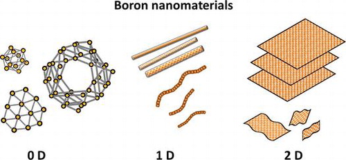
Various types of zero, one, and two-dimensional boron nanomaterials such as nanoclusters, nanowires, nanotubes, nanobelts, nanoribbons, nanosheets, and monolayer crystalline sheets named borophene have been experimentally synthesized and identified in the last 20 years. Owing to their low dimensionality, boron nanomaterials have different bonding configurations from those of three-dimensional bulk boron crystals composed of icosahedra or icosahedral fragments. The resulting intriguing physical and chemical properties of boron nanomaterials are fascinating from the viewpoint of material science. Moreover, the wide variety of boron nanomaterials themselves could be the building blocks for combining with other existing nanomaterials, molecules, atoms, and/or ions to design and create materials with new functionalities and properties. Here, the progress of the boron nanomaterials is reviewed and perspectives and future directions are described.
Classification:
1. Introduction
Boron is a promising material in a wide range of fields, such as high-temperature devices and lightweight reinforcing fillers, because of its high hardness, low density, and high melting point (above 2000 °C)[Citation1–3]. Boron is also a unique material with structural complexity owing to its electron-deficient nature, and thus the allotropes of boron are constituted by large-sized unit cells with several atoms in every case. The common feature of three-dimensional (3D) bulk structures of boron is that they are composed of the building blocks of B12 icosahedra or icosahedral fragments. The bonding in B12 icosahedra is thought to be achieved by the so-called three-center electron-deficient bonds originating from the three valence electrons of boron, where the electron charge is accumulated at the center of a triangle formed by three adjacent boron atoms [Citation2,4,5].
On the other hand, boron is similar to carbon in terms of its capability to form stable covalently bonded molecular networks. Therefore, in parallel with the development of carbon nanomaterials, extensive studies have also been conducted for boron nanomaterials. As early research, in 1966, Olempska et al. [Citation6] reported boron whiskers and needles synthesized by the reduction of boron trichloride with hydrogen at 1300–1800 °C. In 1988–1991, Komatsu et al. [Citation7–12] reported the synthesis of boron films, whiskers, ribbons, and platelets by several experimental methods. Subsequently, boron nanowires, nanotubes, nanoribbons, nanobelts, and/or nanosheets were theoretically predicted in the late 1990s [Citation13–19], followed by the experimental realizations of these boron nanomaterials with detailed analysis of the elements, structures, and/or electronic states from several groups [Citation20]. In the structures of the predicted boron nanomaterials based on the Aufbau principle, the B12 icosahedra building blocks are no longer included, owing to their low dimensionality, which results in unusual bonding and intriguing physical and chemical properties [Citation13–45].
One of the recent focal points of boron nanomaterial research is the experimental realization of a single-atomic two-dimensional (2D) layer of boron named borophene by growing the physically evaporated boron atoms on Ag(111) in ultra-high vacuum [Citation46–48]. After the emergence of borophene, several theoretical works about borophene have been reported [Citation49–78], as well as the experimental discovery of the Dirac fermion in borophene on Ag(111) [Citation79].
Specific advantages of the boron nanomaterials, including borophene, for applications such as hydrogen storage, batteries, catalysts, electronics, superconductors, and/or mechanically strong components have been demonstrated, predicted, and/or discussed together with novel structural, electronic, thermal, optical, and mechanical properties [Citation20,49–78,80,81].
In this review, the progress of the boron nanomaterials is described by focusing on experimental reports especially for the synthesis method and its characterization results rather than theoretical predictions. Here, the boron nanomaterials are classified by the following three categories: zero-dimensional (0D), one-dimensional (1D), and 2D boron nanomaterials. The perspective and future directions for boron nanomaterials are then described.
2. Zero-dimensional (0D) boron nanomaterials
In the case of carbon, fullerene (C60) or higher fullerenes (such as C70, C72, and C76) are often considered as representative 0D nanomaterials, in contrast to the 1D carbon nanotube, 2D graphene, and 3D graphite. However, other small molecules and/or clusters can also be categorized as 0D nanomaterials in terms of the dimensionality in the physical and chemical properties due to their smaller size.
In the case of boron, the Lai-Sheng Wang group systematically elucidated the structures and chemical bonding of size-selected boron clusters produced in gas phase (in vacuum) based on the photoelectron spectroscopy in combination with computational chemistry [Citation24,82–98]. They studied small boron nanoclusters (composed of fewer than 100 B atoms) by comparing small carbon nanoclusters in terms of bonding and structure. For example, all-boron nanotubes [Citation86], all-boron analogues of naphthalene [Citation97], polyenes [Citation90], anthracene [Citation91], phenanthrene [Citation91], and coronene [Citation96] have been observed in their size-selected boron clusters in gas phase and examined in detail to elucidate the structure and bonding by comparing with those of carbon nanoclusters. According to their review [Citation92,98], small atomic boron clusters have planar or quasi-planar structures, stabilized by localized two-center–two-electron (2c–2e) σ bonds on the periphery and delocalized multicenter–two-electron (nc–2e) bonds in both σ and π frameworks. Among the observed clusters, a particularly interesting cluster is B36, which has been found to possess a planar structure with a central hexagonal vacancy [Citation94]. The hexagonal B36 can be viewed as a repeating unit to assemble boron monolayers. These findings provide the first indirect experimental evidence that 2D boron nanomaterials, borophenes, with hexagonal vacancies are potentially viable. Another exciting discovery has been the observation and characterization of the first all-boron fullerenes [Citation95]. Photoelectron spectroscopy revealed that the B40− cluster consisted of two isomers with very different electron binding energies. Global minimum searches led to two nearly degenerate isomers competing for the global minimum: a quasi-planar isomer and an unprecedented cage isomer. In the neutral state, the B40 cage is overwhelmingly the global minimum, the first all-boron fullerene to be observed, and is named ‘borospherene’ [Citation95,98]. There is evidence that there exists a family of borospherenes with B28 being the smallest borospherene [Citation95,98]. It is expected that the pace of discovery will continue to accelerate in boron clusters, and more interesting structures and chemical bonds will be uncovered with heightened research interests and more sophisticated experimental and computational methods [Citation92,98].
In contrast to the great progress in understanding such small boron nanoclusters, the synthesis of these nanoclusters has not yet been established. This is in sharp contrast to the 1D and 2D boron nanomaterials, where production is realized by several methods and superior properties for the applications are shown as described below.
3. One-dimensional (1D) boron nanomaterials
3.1. Boron nanowires
Nanowires have potential for applications in the electronics field by assembling them as nanoscale electric wires. Thermal and chemical stabilities and uniform conductivity, as well as mechanical strength, are important factors for such applications which are closely related to the morphology and structure of the nanowires. Nanowires are also useful as electron sources by field emission, where the stabilities are again a crucial issue, as well as the tip structure. Boron nanowires were experimentally synthesized earlier among the boron nanomaterials by several experimental methods, which can be classified into three types: chemical vapor deposition (CVD), radio frequency magnetron sputtering, and laser ablation, as summarized in a previous review by Tian et al. [Citation80]. The shape, structure, and bonding nature of synthesized boron nanowires are different depending on the synthesis methods. In any method, the growth of boron nanowires requires a high temperature (500–1500 °C) and the resulting boron nanowires with diameters of 10–300 nm tend to form crystalline structures if the growth is assisted by a catalyst, while amorphous boron nanowires are formed in the absence of a catalyst [Citation80]. In this review, boron nanowires are summarized by classifying amorphous and crystalline boron nanowires with their growth mechanism. The applications of boron nanowires are then briefly introduced.
3.1.1. Synthesis of amorphous boron nanowires
Amorphous boron nanowires with several μm length and 50–100 nm diameter were first synthesized and clearly identified by Wu et al. in 2001 [Citation99]. Scanning electron microscopy (SEM) and transmission electron microscopy (TEM) images of their nanowires are shown in Figure (a) and (b). The nanowires were obtained as black product by growing on MgO substrate in a sealed quartz tube under BI3 vapor at 1000–1100 °C under evacuated condition at 100 mTorr. More specifically, powders of Si, I2, and B were put in one end of the tube and a MgO substrate coated by a 5-nm Au thin film was placed in the other end of tube, where a temperature gradient of 100 °C was maintained between source materials and the MgO substrate. At the hot zone, boron reacts with I2 and forms BI3 vapor. The vapor then decomposed in the low temperature zone to form boron nanowires on MgO. The obtained boron nanowires are amorphous and thus no diffraction spots or rings were observed, even by selected area electron diffraction (SAED). The nanowire tips were composed of Au, B, and Si, while the bodies of the nanowires were composed of B with a small amount of Si, as shown by the electron energy loss spectroscopy (EELS) results (Figure (c)). Based on the presence of the droplet of B/Au/Si alloy at the tip, the growth mechanism was suggested as a vapor-liquid-solid (VLS) process with Au as the liquid solvent at high temperature. The authors pointed out that the presence of Si is important to form boron nanowires because nanowires are not formed if Si was removed from the starting materials. The authors used the obtained boron nanowires as an intermediate product for the synthesis of MgB2 nanowires [Citation99].
Figure 1. Amorphous boron nanowires synthesized by CVD method. (a) SEM image of the boron nanowires. (b) TEM image of the boron nanowires. The inset shows the tip of one nanowire. (c) EELS spectrum recorded on the boron nanowires. Reproduced from Ref. [Citation99] by permission of John Wiley & Sons Ltd.
![Figure 1. Amorphous boron nanowires synthesized by CVD method. (a) SEM image of the boron nanowires. (b) TEM image of the boron nanowires. The inset shows the tip of one nanowire. (c) EELS spectrum recorded on the boron nanowires. Reproduced from Ref. [Citation99] by permission of John Wiley & Sons Ltd.](/cms/asset/fd8c480d-aa04-4aec-b9b9-53b4755bb0f4/tsta_a_1379856_f0001_b.gif)
Subsequently, well-aligned amorphous boron nanowire arrays were synthesized by Cao et al. [Citation100] in 2001 in an argon atmosphere by a simple method of radio frequency magnetron sputtering (80 W at 800 °C and 2 Pa for 6 hours), with a target of highly pure boron and a boron oxide mixture (the authors concluded that boron nanowire arrays can also be formed without boron oxide). Citation[100]Boron nanowires with diameters of 20–80 nm and lengths of up to several tens of micrometers stand on the substrate Si surface to form well-aligned arrays with self-organized arrangements (Figure (a)–(c)). The nanowire arrays can easily be stripped off (Figure (a)) with tweezers, suggesting that the boron nanowires are not strongly chemically bonded to the substrate surface. Most of the tips of wires are flat rather than hemispherical in morphology (Figure (c)). The TEM and SAED analysis for the boron nanowire peeled off from the arrays show a flat and smooth morphology and amorphous structure (Figure (d)). The amorphous phase was further confirmed by high-resolution TEM. The composition of the nanowires was revealed to be boron with a small amount of oxygen (less than 5%) based on EELS analysis (Figure (e)). The nanowire arrays in Figure are then concluded to be composed dominantly by boron atoms and no metal elements are included, which is in sharp contrast to the case of nanowires shown in Figure .The authors pointed out that a high temperature at the substrate surface (above 700 °C) plays a crucial role in the nucleation and growth of boron nanowires, because the nanowire growth was not observed below 600 °C [Citation100,101]. The growth of boron nanowire arrays is insensitive to the nature of the substrate, because the same size and shape of the boron nanowires were observed after the growth on Si(100), Si(111), SiO2, metal plates (Ni, Fe, Co), and metal films (Pd, Au, Ag) on Si. The nucleation and growth of vertically aligned boron nanowires arrays are thus concluded to be entirely self-organized rather than catalyst-assisted processes. Interestingly, merely by increasing the Ar flow rate to 60 cm3 min−1 (by a factor of approximately two) in the radio frequency magnetron sputtering process, boron nanofeather-like arrays are grown, where each boron wire possesses Y and/or T junctions [Citation102]. The authors concluded that this process might enable the creation of nanometer-size heterojunctions of a wide variety of one-dimensional (1D) nanostructures [Citation103]. Since no crystallization was observed up to a pressure of 103.5 GPa for these boron nanowires, the amorphous structure of boron nanowires is concluded as stable under high pressure at ambient temperature [Citation104]. Here, it should be noted that according to a subsequent report by Wang and Duan [Citation105], the amorphous structure of boron nanowires made by a similar radio frequency magnetron sputtering method can be converted to a rhombohedral crystalline structure (β-boron) with lattice parameters of a = 10.95 Å and c = 23.82 Å by annealing at 1050 °C under a high vacuum for 3 hours followed by a quench. Citation[105]Additionally, Gao et al. [Citation106] reported that crystalline boron nanowires with 10 nm diameter can be directly synthesized by the same method of the radio frequency magnetron sputtering if Au catalysts are present via a VLS growth mechanism even at a lower temperature of 600 °CCitation[106]. Concerning the boron nanojunction, later works show that nanojunctions can also be formed by a thermal vapor transfer method [Citation107,108] and an oxide-assisted VLS process [Citation109].
Figure 2. Amorphous boron nanowire arrays synthesized by the radio frequency magnetron sputtering method. (a) Low-magnification SEM image of the aligned boron nanowire arrays grown on Si substrates. (b) Cross-sectional SEM image. (c) High-magnification SEM image. Most of the boron nanowire tips have a platform-shaped morphology with a diameter of 60 ± 80 nm. (d) TEM image of a typical boron nanowire. Inset, SAED pattern taken from the nanowire showing some amorphous halo rings. (e) EELS spectra; a) boron nanowire; b) bulk, pure boron; c) bulk B2O3. The insets are magnified features of the O-K edges. Reproduced from Ref. [Citation100] by permission of John Wiley & Sons Ltd.
![Figure 2. Amorphous boron nanowire arrays synthesized by the radio frequency magnetron sputtering method. (a) Low-magnification SEM image of the aligned boron nanowire arrays grown on Si substrates. (b) Cross-sectional SEM image. (c) High-magnification SEM image. Most of the boron nanowire tips have a platform-shaped morphology with a diameter of 60 ± 80 nm. (d) TEM image of a typical boron nanowire. Inset, SAED pattern taken from the nanowire showing some amorphous halo rings. (e) EELS spectra; a) boron nanowire; b) bulk, pure boron; c) bulk B2O3. The insets are magnified features of the O-K edges. Reproduced from Ref. [Citation100] by permission of John Wiley & Sons Ltd.](/cms/asset/41f4010b-9768-417b-9b1b-487e22767425/tsta_a_1379856_f0002_b.gif)
Meng et al. [Citation110] reported the synthesis of amorphous boron nanowires with diameters of 30–60 nm and lengths of several tens of micrometers by a laser ablation methodCitation[110]. A KrF excimer laser with a wavelength of 248 nm and a frequency of 10 Hz was used to continuously ablate the target of pure boron in an alumina tube at 1300 °C for 5 hours under vacuum with Ar flow (laser energy of 350 mJ per pulse and a pulse duration of 34 ns). Owing to the fact that the target material is only boron powder, the authors concluded that the growth of B nanowires is governed by a vapor-solid (VS) process rather than a VLS process.
Yang et al. [Citation111] demonstrated control over the morphology and diameter of amorphous boron nanowires, in CVD with VLS growth on silicon substrates, by altering the growth temperature and the thickness of the catalyst Au films on the substrate. A mixture of nitrogen, hydrogen, and diborane with a flow ratio of 10:50:1 was introduced in the quartz tube with Au-coated Si substrate at 750–1000 °C and 5 × 10⁴ Pa for 5 hours. Smooth boron nanowires were fabricated at a temperature ranging from 800 to 900 °C (Figure ). The diameter of boron nanowires increased slightly from 10 to 50 nm as the growth temperature increased (Figure (f)). Boron nanochains with the periodically modulated diameter were also fabricated at 950 °C (Figure (d)). As the thickness of the Au films on the Si substrate increases, the diameter and length of the boron nanowires increase dramatically.
Figure 3. Size control of the diameter of amorphous boron nanowires in CVD method. TEM images of the boron nanowires synthesized at (a) 750 °C, (b) 800 °C, (c) 900 °C, and (d) 950 °C, respectively, while the thickness of the Au film catalyst was 5 nm. (e) A typical diameter histogram for the boron nanowires prepared at 800 °C. (f) Mean diameter of the boron nanowires as a function of temperature. Reproduced from Ref. [Citation111] by permission of SpringerVerlag.
![Figure 3. Size control of the diameter of amorphous boron nanowires in CVD method. TEM images of the boron nanowires synthesized at (a) 750 °C, (b) 800 °C, (c) 900 °C, and (d) 950 °C, respectively, while the thickness of the Au film catalyst was 5 nm. (e) A typical diameter histogram for the boron nanowires prepared at 800 °C. (f) Mean diameter of the boron nanowires as a function of temperature. Reproduced from Ref. [Citation111] by permission of SpringerVerlag.](/cms/asset/d4b17e76-57ff-49d0-909b-f01cf783cbf6/tsta_a_1379856_f0003_b.gif)
3.1.2. Synthesis of crystalline boron nanowires
In parallel with the first reports on amorphous boron nanowires in 2001 [Citation99,100], crystalline boron nanowires were synthesized and identified by Otten et al. (CVD) [Citation112] and Zhang et al. (laser ablation) in 2002 [Citation113].
In the report by Otten et al. (CVD method), a mixture of 5% diborane (B2H6) in Ar gas was passed at a rate of 15 mL/min for 30 minutes over NiB powder on an alumina substrate in a tube furnace at 1100 °C [Citation112]. The resulting brittle slag has dense entanglements of nanowires (Figure (a) with diameters ranging from 20 to 200 nm (mean value ~60 nm) (Figure (b) and (c)). Based on an electron diffraction pattern (Figure (d)), the nanowires were concluded as dense, twinned, whisker crystals with an orthorhombic unit cell of a = 9.4 Å, b = 7.1 Å, and c = 5.4 Å. The conductivity measurements of individual nanowires show semiconducting character with (1.3–5.5) × 10−5 (ohm cm)−1, which is in the range of 10−4–10−7(ohm cm)−1 reported as that for bulk B.
Figure 4. Crystalline boron nanowires. Synthesized by CVD method: (a) SEM image of B nanowires, (b), (c) TEM images, and (d) electron-diffraction pattern of nanowire in (c). Reprinted with permission from Ref [Citation112]. Copyright 2002 American Chemical Society. (e) High-resolution TEM image and its corresponding SAED. Reprinted from Ref. [Citation114]. Copyright 2004 with permission from Elsevier. (f) TEM image of dispersive boron nanowires. The upper right inset is the corresponding SAED pattern of the arrowed boron nanowire. (g) High-resolution TEM image of the arrowed boron nanowire, revealing its single-crystal structure. Reprinted from Ref. [Citation115]. Copyright 2004 with permission from Elsevier.
![Figure 4. Crystalline boron nanowires. Synthesized by CVD method: (a) SEM image of B nanowires, (b), (c) TEM images, and (d) electron-diffraction pattern of nanowire in (c). Reprinted with permission from Ref [Citation112]. Copyright 2002 American Chemical Society. (e) High-resolution TEM image and its corresponding SAED. Reprinted from Ref. [Citation114]. Copyright 2004 with permission from Elsevier. (f) TEM image of dispersive boron nanowires. The upper right inset is the corresponding SAED pattern of the arrowed boron nanowire. (g) High-resolution TEM image of the arrowed boron nanowire, revealing its single-crystal structure. Reprinted from Ref. [Citation115]. Copyright 2004 with permission from Elsevier.](/cms/asset/238b469c-da11-4fa6-ac77-885cf2312d44/tsta_a_1379856_f0004_b.gif)
On the other hand, in the reports by Zhang et al. [Citation113,114], single- and poly-crystalline boron nanowires were obtained as a part of the product of laser ablationCitation[113], [114]. A mixture of boron rods with Ni and Co powder was placed as a target in a furnace kept at 1250 °C in a vacuum with Ar flow. A Nd:YAG laser was used for ablation of the target for 30 minutes with 532 nm wavelength, 10 Hz frequency, and 3.5 W power. Nanowires with a diameter less than 100 nm were then observed by SEM and TEM to be grown at the surface of the target. SAED analysis suggests that a portion of the nanowires are single crystal of tetragonal structure with lattice parameters of a = 0.875 nm and c = 0.506 nm (Figure (e)). At one end of the nanowire, a droplet composed of B, Ni, and Co was observed, indicating the VLS mechanism for growing boron nanowires. They concluded that the boron nanowires with diameters ranging from several tens of nanometers to 1 μm can be synthesized by the laser ablation method on the surfaces of the targets, where the synthesis temperatures, intensities of the laser beams, and types of metal catalysts are the main synthesis effect factors on the growth.
Subsequently, well-aligned boron nanowires with single-crystalline structure were reported by Yang et al. in 2003 [Citation115], using nanochannel-Al2O3 as a substrate and a CVD process. The nanochannel-Al2O3 was placed in a quartz tube furnace chamber and a mixture of Ar, H2, and diborane with a flow rate of 10:10:1 was allowed into the chamber, which was maintained at 1500 Pa and 800 °C. The nanochannel-Al2O3 substrate with deposited materials was then dissolved in a dilute 1 M NaOH solution at 60 °C. Finally, the solution was dropped onto a copper grid for TEM measurements. Figure (f) is a TEM image of dispersed boron nanowires with a diameter of 25 nm. The SAED pattern illustrates that the nanowire is a single crystal tetragonal lattice structure of elemental boron with the lattice constants of a = 0.873 nm and c = 0.503 nm (inset in Figure (f)), which are nearly the same as the lattice parameters of the boron nanowire prepared by laser ablation as described above [Citation113]. The distance between the parallel fringes of boron nanowire observed in high resolution TEM image (Figure (g)) is approximately 0.45 nm, corresponding to the spacing of the {1 1 0} planes of B with a structure. The proposed formation mechanism is as follows: first, diborane gas decomposed into boron atom clusters and H2 gas, and boron atoms reacted with the c-Al2O3 of a nanochannel-Al2O3 substrate and formed Al5BO9 layer on the surface of the channels of the nanochannel-Al2O3, which then prevented boron from reacting with Al2O3. After that, boron clusters conglomerated to generate boron nanowires by confinement of the channels of the nanochannel-Al2O3 substrate.
As described above, the different structure types of the crystalline boron nanowires, i.e. rhombohedral (β-boron) [Citation105,116], orthorhombic [Citation112], and tetragonal [Citation113,114] structures, are formed depending on the synthesis method and conditions. The method to control the growth type of crystal structure of boron nanowires has not yet been well established. However, concerning the quality of the crystalline structure, Yun et al. [Citation117] reported that single-crystalline boron nanowires of a rhombohedral structure (a = 10.94 Å and c = 23.83 Å) and (031) orientation aligned along the normal of the substrates can be predominantly synthesized by higher-temperature (⩾1100 °C) processing of a thermal vapor transport if it was followed by a quenchCitation[117]. In the SEM images and X-ray diffraction (XRD) patterns in Figure , a sharp contrast can be found between the cases for slow cooling of ~5 °C/min and quench after synthesizing boron nanowires at 1100 °C for 30 minutes, indicating a significant effect of quenching on the improvement of crystallinity and alignment of boron nanowires.
Figure 5. Effect of quenching on crystallinity and alignment of boron nanowires. SEM images (scale bar 10 μm) and XRD patterns of boron nanowires film synthesized at 1100 °C for 30 minutes followed by (a)(c) slow cooling of ~5 °C/min and (b)(d) quench, respectively. Reprinted with permission from Ref. [Citation117]. Copyright 2004 American Institute of Physics.
![Figure 5. Effect of quenching on crystallinity and alignment of boron nanowires. SEM images (scale bar 10 μm) and XRD patterns of boron nanowires film synthesized at 1100 °C for 30 minutes followed by (a)(c) slow cooling of ~5 °C/min and (b)(d) quench, respectively. Reprinted with permission from Ref. [Citation117]. Copyright 2004 American Institute of Physics.](/cms/asset/6b52769c-de49-4eee-a93a-d4a4270e0a0d/tsta_a_1379856_f0005_b.gif)
3.1.3. Applications of boron nanowires
The excellent mechanical properties of individual crystalline boron nanowires have been reported by a few groups [Citation118–122]. According to the report by Liu et al. in 2013 [Citation122], the mean fracture strength and the maximum strain of individual crystalline boron nanowires prepared by CVD method (α-tetragonal lattice, [001] growth direction) were measured to be 10.4 GPa and 4.1%, respectively, during the tensile testsCitation[122]. The average Young’s modulus was calculated to be 308.2 GPa under tensile and compression tests. Bending experiments for individual boron nanowires revealed that their maximum bending strain could reach 9.9% (Figure ) and their ultimate bending stress occurred at 36.2 GPa. These values are much higher than those of Si and ZnO nanowires, which are known for their high bending strength. The boron nanowires also show a very high specific fracture strength of 3.9 GPa·cm3/g and specific elastic modulus of 130.6 GPa·cm3/g, which are one to two orders of magnitude larger compared to many reported nanostructures [Citation122]. These results suggest that the boron nanowires are a promising material for application as lightweight reinforcing fillers.
Figure 6. Consecutive TEM images of an individual boron nanowire during different bending stages. Reprinted with permission from Ref. [Citation122]. Copyright 2013 American Chemical Society.
![Figure 6. Consecutive TEM images of an individual boron nanowire during different bending stages. Reprinted with permission from Ref. [Citation122]. Copyright 2013 American Chemical Society.](/cms/asset/50c229e7-844e-44a6-8e90-551582c3ec9d/tsta_a_1379856_f0006_oc.gif)
The excellent field emission properties of boron nanowires, such as low turn-on field and high current endurance, have been reported [Citation123–129]. For practical applications in field emission displays, there are two important additional issues: (i) patterned growth of boron nanowire arrays over a large area; and (ii) uniformity of physical properties of grown boron nanowires. According to the report by Liu et al. in 2014 [Citation129], uniform crystalline boron nanowires (α-tetragonal lattice and the growth direction along the [001] orientation) with square (25 μm × 60 μm) patterns have been grown over a large area by CVD on a Si substrate with Ni catalysts patterned by an ultraviolet lithography technique (Figure (a) and (b)) and the patterns show bright and uniform performance of field emissionCitation[129]. The side view in Figure (c) shows the high and uniform density of boron nanowires in each square of their prepared pattern. Most of the boron nanowires have an average length of approximately 6 μm with a uniform diameter of 30–40 nm (Figure (c) and (d)). There are no catalysts at the tips of the boron nanowires (Figure (e)), while Ni catalysts exist between the ends of the boron nanowires and the substrate (shown as white circles in Figure (f)), indicating that the boron nanowires are formed by a base-up growth mode. The authors also measured I–V curves of individual boron nanowires and estimated the electronic conductivity as 1.66 × 10⁻² (ohm cm)−1 which is a few orders of magnitude greater than that of bulk B of 10−4–10−7(ohm cm)−1. For the patterned boron nanowires, a turn-on field of 4.3 V/μm (at 10 μA/cm2 emission current density) and a threshold field of 10.4 V/μm (at 1 mA/cm2 emission current density) have been reported. These values are comparable to those of many excellent cathode nanomaterials, such as ZnO nanowires, WO3 nanowires, and AlN nanowires, but are inferior to those of carbon nanotubes, graphene, and LaB6. Figures (g) and (h) show field emission images of patterned boron nanowires at a current density of 1.4 mA/cm2 and 2.1 mA/cm2. Nearly all patterns are simultaneously involved in the emission process and the emission brightness increases with the emission current density. It is worth noting that both the distribution of the emission patterns and their brightness distribution are very uniform owing to the uniform growth of boron nanowires.
Figure 7. (a) SEM image of crystalline boron nanowire patterns. (b) Side view SEM image of uniform boron nanowire patterns. (c), (d) Side view SEM image of boron nanowires at the edge and at the inner portion of the pattern. (e), (f) SEM images of the tip and the end of boron nanowires. The white circles indicate the catalysts’ sites. (g), (h) Field emission images of patterned boron nanowires at a current density of 1.4 mA/cm2 and 2.1 mA/cm2. Reproduced from Ref. [Citation129] by permission of John Wiley & Sons Ltd.
![Figure 7. (a) SEM image of crystalline boron nanowire patterns. (b) Side view SEM image of uniform boron nanowire patterns. (c), (d) Side view SEM image of boron nanowires at the edge and at the inner portion of the pattern. (e), (f) SEM images of the tip and the end of boron nanowires. The white circles indicate the catalysts’ sites. (g), (h) Field emission images of patterned boron nanowires at a current density of 1.4 mA/cm2 and 2.1 mA/cm2. Reproduced from Ref. [Citation129] by permission of John Wiley & Sons Ltd.](/cms/asset/cd1e64b1-cac7-43d4-9326-262496b330a0/tsta_a_1379856_f0007_b.gif)
3.2. Boron nanotubes
After several theoretical studies in 1990s predicted the structure and intriguing properties of boron nanotubes, such as metallic conductivity exceeding that of carbon nanotubes [Citation10–16], the CVD synthesis of a pure boron single-wall nanotube was reported by Ciuparu et al. in 2004 [Citation130]. They used a magnesium-substituted mesoporous silica template (Mg–MCM-41) as a catalyst and a mixture of BCl3 and H2 gases (volumetric ratio of approximately 1:6) as a source. The gas mixture was introduced at a rate of 1.5 L/min for 45 minutes in a quartz reactor (inner diameter 6 mm) with the Mg–MCM-41 catalyst at a steady state temperature of 870 °C under a continuous flow of hydrogen. The reactor was then cooled to room temperature under He flow. Figure (a) (inset) shows a TEM image of the single-wall boron nanotube obtained on the catalyst, which shows a tubular structure. The Raman spectrum shown in Figure (a) contains distinct peak at 210 cm−1, which was attributed to the characteristic radial breathing mode of the tubular structure. The author also attributed the spectral features between 300 and 500 cm−1 (peak b) to tubular structures. Based on EELS results, the structure is revealed to be composed of pure boron. Thus, the observed structure is concluded as a pure boron single-wall nanotube. For the synthesis method, the authors pointed out the importance of the presence of Mg in the catalyst, since no boron nanotube formation was observed when they used a pure siliceous MCM-41.
Figure 8. (a) Raman spectrum and TEM image (inset) of boron nanotube. Owing to the extreme beam sensitivity and charging of the sample, the image is blurred and out of focus. Reprinted with permission from Ref. [Citation130]. Copyright 2004 American Chemical Society. (b) Low-magnification SEM image of large-area boron nanostructures. (c) Magnified SEM image of the boron nanostructures. (d) SEM image of a boron nanotube tip. (e) High-resolution SEM image of the boron nanowires and boron nanotubes at the growth stage. Black and white arrows indicate a boron nanotube and a boron nanowire, respectively. Reproduced from Ref. [Citation131] by permission of The Royal Society of Chemistry.
![Figure 8. (a) Raman spectrum and TEM image (inset) of boron nanotube. Owing to the extreme beam sensitivity and charging of the sample, the image is blurred and out of focus. Reprinted with permission from Ref. [Citation130]. Copyright 2004 American Chemical Society. (b) Low-magnification SEM image of large-area boron nanostructures. (c) Magnified SEM image of the boron nanostructures. (d) SEM image of a boron nanotube tip. (e) High-resolution SEM image of the boron nanowires and boron nanotubes at the growth stage. Black and white arrows indicate a boron nanotube and a boron nanowire, respectively. Reproduced from Ref. [Citation131] by permission of The Royal Society of Chemistry.](/cms/asset/1cbf2fb9-7700-436b-81a2-22a528a2cdf8/tsta_a_1379856_f0008_b.gif)
The fabrication of a larger quantity of crystalline boron nanotubes was reported by Liu et al. in 2010 [Citation131]. They synthesized boron nanotubes with diameters ranging from 10 to 40 nm and an average length of several micrometers by growing on Fe3O4 nanoparticles with diameters less than 10 nm through high-temperature solution phase reaction at 1000–1200 °C for 4 hours, where a mixture of B2O3 and boron powders with mass ratio of 4:3 was used as the source material. Figure (b) shows the densely packed boron nanostructures on the silicon substrate, with lengths in the range of 2–4 μm. A typical high-resolution SEM image of the boron nanotubes is shown in Figure (c), in which some boron nanowires are mixed in the product. A side view of a typical boron nanotube is given in Figure (d), showing that the free end of the boron nanotube is open. A SEM image of the synthesized product with a growth time of 10 minutes is shown in Figure (e). The white and black arrows indicate the short boron nanotubes and boron nanowires, respectively, which coexisted at the early stage of growth. Initial growth precursors of the boron nanotubes are ascribed to the alloy nanodroplets of boron-magnetite and boron nanostructures are believed to be grown by the root-growth VLS mechanism. Based on the SAED pattern, the boron nanowires are revealed to be composed of perfect single crystals with an α-tetragonal structure and their growth direction is along [001]. The as-synthesized boron nanotubes are multi-layered nanotubes with the spacing between two adjacent layers of approximately 3.2 Å. The measurements of individual boron nanotubes show that the conductivity is in the order of 102 (ohm cm)−1, showing the metallic transport property of boron nanotubes. The conductivity is four orders of magnitude larger than that of the largest conductivity of boron nanowires described above. The individual boron nanotube also shows excellent field emission properties, with a high stable current of approximately 80 μA and a current density of 2 × 10¹¹A/m2 which are very close to those of carbon nanotubes.
3.3. Boron nanobelts and nanoribbons
Nanobelts and nanoribbons are materials that are macroscopically categorized as 1D rather than 2D (nanosheets), since they have a rectangular cross-sectional shape and have a width-to-thickness ratio greater than one, which is also different from simple 1D tubes or wires. Nanoribbons have significantly larger width-to-thickness ratios (10–100) compared with nanobelts (~5), and thus they should have different chemical and physical properties, depending on their size and shape as well as their bonding nature.
3.3.1. Boron nanobelts
The synthesis of single-crystalline tetragonal boron nanobelts was first reported by Wang et al. in 2003 [Citation132]. They synthesized boron nanobelts by a laser ablation method (Nd:YAG laser with 355 nm wavelength, pulse width of 5–7 ns and 10 Hz pulse frequency) in a furnace without using a catalyst or boron vapor. The laser was introduced through a quartz glass window to the target of a hot-pressed boron pellet on a rotating holder placed at the center of the furnace. The boron nanostructures were deposited on the quartz glass substrate at 800 °C under Ar flow at 25 Pa. A TEM image of a typical obtained boron nanobelt (Figure (a)) shows flat edges without the presence of nanoparticles and inhomogeneity, where EELS confirm that the nanobelts are composed of boron. Boron nanobelts have a width-to-thickness ratio of approximately 5 (several tens of nanometers to approximately 150 nm) and several micrometers to the order of millimeters in length. Figures (b) and (c) show the boron nanobelt with tetragonal crystalline structure (a = 0.884 nm and c = 0.500 nm, [001] growth direction) with 55 nm width, where an amorphous structure can be seen along the surface of the nanobelt with 2–4 nm thickness. Some stacking faults were also observed along the growth direction, as shown by black arrows in Figure (c). The authors explained that the growth was progressed by an oxide-assisted-growth (OAG) mechanism, in which an oxide layer is presumed to be molten or near-molten, which might enhance atomic absorption, diffusion, and desorption. The synthesized crystalline boron nanobelts were revealed to be p-type semiconductors with electrical conductivity of the order of 10−3 (ohm cm)−1 at room temperature, which can be enhanced by a factor of 100–500 by doping Mg [Citation133–135].
Figure 9. (a) TEM image of a boron nanobelt tip. (b) TEM image of a 55 nm-wide boron nanobelt. The surface of this nanobelt is sheathed with amorphous phase, as indicated by white arrows. (c) TEM image of white rectangular region in (b). Some stacking faults, indicated by black arrows, can be seen along the growth direction. A detailed analysis of the corresponding electron diffraction pattern shown in the inset indicated that the crystal structure is tetragonal and the growth direction of this nanobelt is the [001] direction. Reprinted from Ref. [Citation132]. Copyright 2003 with permission from Elsevier.
![Figure 9. (a) TEM image of a boron nanobelt tip. (b) TEM image of a 55 nm-wide boron nanobelt. The surface of this nanobelt is sheathed with amorphous phase, as indicated by white arrows. (c) TEM image of white rectangular region in (b). Some stacking faults, indicated by black arrows, can be seen along the growth direction. A detailed analysis of the corresponding electron diffraction pattern shown in the inset indicated that the crystal structure is tetragonal and the growth direction of this nanobelt is the [001] direction. Reprinted from Ref. [Citation132]. Copyright 2003 with permission from Elsevier.](/cms/asset/ad555660-e2d5-444e-8439-1db73252b34d/tsta_a_1379856_f0009_b.gif)
In 2008, α-tetragonal crystalline boron nanobelts with [001] growth axis were also reported to be synthesized by combining the methods of e-beam evaporation and plasma ion bombardment [Citation136]. Here, the boron was evaporated on an oxidized silica substrate coated with Au, which was heated to 1100 °C followed by bombardment via a helicon plasma source. Most of the resulting nanobelts had a width of 0.1–1 μm and a thickness of 50–100 nm, while a few nanometer-sized belts, such as those with a width of 30–100 nm, thickness of 10–15 nm, and length of a few to over 15 μm were also formed.
On the other hand, in 2008, rhombohedral crystalline boron nanobelts with a [Citation111] growth direction and amorphous boron nanobelts were synthesized separately by controlling the condition of the method with a vapor-liquid-solid technique by Ni and Li [Citation137]. Here, a mixture of boron, silicon, and iodine powders with the weight ratio 40:1:1 was placed into a smaller quartz boat and placed at one end of a quartz tube of diameter 19.05 mm, while a single crystal Si(100) substrate was placed at the other end of the tube after coating with a 3- or 20-nm Au film (the former was used for crystalline boron nanobelt growth and the latter was used for amorphous boron nanobelt growth). Crystalline boron nanobelts were grown on Si(100) at 1100 °C with the source maintained at 1150 °C [Citation137]. Most of the crystalline nanobelts have a width-to-thickness ratio of 2 and are covered with a layer of amorphous silicon oxide. Amorphous boron nanobelts were grown when the Si substrate temperature was 1050–1070 °C. From these results, the authors pointed out that the temperature gradient in the system is an important factor in addition to the high cooling rate to achieve crystalline boron nanobelts.
3.3.2. Boron nanoribbons
In 1990, Komatsu and Moriyoshi [Citation9] reported that β-rhombohedral boron nanoribbons were synthesized on a Si(100) substrate, as well as whiskers and platelets by plasma-enhanced CVD with 2 kW from a gas mixture of B2H6 (0.25–1.5 vol%), H2 (5–30 vol%), and He at 700–880 °C, where the flexible ribbon-like morphology was observed by SEM, though the precise width-to-thickness ratio was not examinedCitation[9].
On the other hand, in 2004, single-crystalline α-tetragonal boron nanoribbons of a width of 200–500 nm and thickness of ~20 nm were synthesized at low temperature (630–750 °C) and low pressure (200 mTorr) by pyrolysis of diborane gas in a quartz tube furnace without a catalyst by Xu et al. [Citation138]. The nanoribbons were confirmed by EELS to be composed of boron. SEM images show that the nanoribbons are typically twisted and the edges of ribbons are sometimes not straight, but rather a zigzag shape. By applying the same method, crystalline α-tetragonal boron nanoribbons of thickness 16 nm were reported to be synthesized by Jash and Trenary in 2009 [Citation139].
3.3.3. Borophene nanoribbons on Ag(110)
In 2017, Zhong et al. reported synthesis of single-atom-thick borophene nanoribbons by self-assembly of boron on Ag(110) surface [Citation140]. More specifically, boron with 99.9999% purity was evaporated using an electron-beam evaporator on the Ag(110) surface, while the surface was kept at a temperature of 570 K in an ultrahigh vacuum with base pressure of 2 × 10⁻¹¹ Torr. The scanning tunneling microscopy (STM) studies reveal high quality borophene nanoribbons: all the ribbons are along the [−110] direction of Ag(110), and can run across the steps on the surface as shown in Figure (a). The width of ribbons is distributed in a narrow range around 10.3 ± 0.2 nm (Figure (b)). High resolution STM images revealed four ordered surface structures in borophene nanoribbons (Figure (c)). Combined with density functional theory (DFT) calculations, authors found that all four structures of borophene nanoribbons (named P1, P2, P3, and P4) consist of the boron chains with different widths, separated by hexagonal hole arrays (Figure ). More specifically, the structures of P1, P2, P3, and P4 are assigned as the same structure of so-called χ3, β12, β, and β8 borophene sheet, respectively, predicted by the previous theoretical study [Citation37]. To represent the nanoribbon character, the authors named them BC(2,2), BC(2,3), BC(3,4), and BC(4,4), respectively, where n and m in BC(n, m) denote the number of atoms in the widest and narrowest regions of a single boron chain.
Figure 10. Borophene nanoribbons on Ag(110) surface. (a) A derivative STM image shows boronphene nanoribbons grown on Ag(110). The image size is 100 × 100 nm2. The nanoribbons run across the substrate steps without losing continuity. (b) Histogram of nanoribbon width. Gaussian fitting is shown as a black line. (c) High-resolution STM image of two boronphene nanoribbons. Image size: 50 × 30 nm2. The bias voltages of STM images are (a) −4.5 V and (b) −1.9 V. Reprinted with permission from Ref. [Citation140]. Copyright 2017 American Physical Society.
![Figure 10. Borophene nanoribbons on Ag(110) surface. (a) A derivative STM image shows boronphene nanoribbons grown on Ag(110). The image size is 100 × 100 nm2. The nanoribbons run across the substrate steps without losing continuity. (b) Histogram of nanoribbon width. Gaussian fitting is shown as a black line. (c) High-resolution STM image of two boronphene nanoribbons. Image size: 50 × 30 nm2. The bias voltages of STM images are (a) −4.5 V and (b) −1.9 V. Reprinted with permission from Ref. [Citation140]. Copyright 2017 American Physical Society.](/cms/asset/ad03e51b-36ff-4f55-9827-cf8c3d9b20f0/tsta_a_1379856_f0010_oc.gif)
Figure 11. Atomic structures of borophene nanoribbons on Ag(110) optimized by DFT. (a)–(d) Top and (e)–(h) side views of optimized P1–P4 borophene nanoribbons on Ag(110) surface, respectively. Color codes: B, small orange spheres; topmost Ag, large white spheres; lower Ag, large blue spheres. (i)–(l) Simulated STM images for P1–P4 based on the calculated electronic density (0–2 eV above the Fermi level). The red frames correspond to the observed unit cells in STM images. Reprinted with permission from Ref. [Citation140]. Copyright 2017 American Physical Society.
![Figure 11. Atomic structures of borophene nanoribbons on Ag(110) optimized by DFT. (a)–(d) Top and (e)–(h) side views of optimized P1–P4 borophene nanoribbons on Ag(110) surface, respectively. Color codes: B, small orange spheres; topmost Ag, large white spheres; lower Ag, large blue spheres. (i)–(l) Simulated STM images for P1–P4 based on the calculated electronic density (0–2 eV above the Fermi level). The red frames correspond to the observed unit cells in STM images. Reprinted with permission from Ref. [Citation140]. Copyright 2017 American Physical Society.](/cms/asset/eab6a466-4de5-44e2-950a-9f117f56de5e/tsta_a_1379856_f0011_oc.gif)
4. Two-dimensional (2D) boron nanomaterials
2D materials consisting of a single or a few layers of atoms exhibit superior performance compared to conventional materials or their bulk counterparts in a variety of applications, because of their unique properties, including their flexibility, high specific surface area, and quasi-2D electron confinement [Citation141–146]. In the case of boron, small clusters with 2D structures were predicted in the 1990s [Citation13–19] and then synthesized in gas phase after 2013 [Citation84,94,147,148], while large-sized boron nanosheets or borophene were synthesized after 2015 [Citation46,47,81,149–153]. The experimental realization of borophene stimulates the theoretical study and several applications of borophene, such as hydrogen storage, batteries, catalysts, electronics, superconductors, and/or mechanically strong components have been predicted together with novel structural, electronic, thermal, optical, and mechanical properties [Citation20,49–78,80,81].
4.1. Boron nanosheets
Xu et al. reported the synthesis and application of ultrathin single-crystalline boron nanosheets [Citation81]. The nanosheets were synthesized on Si wafers by an effective vapor-solid process via thermal decomposition of diborane without catalyst in a 30-mm external-diameter quartz tube at 950 °C by introducing a mixture gas (5% diborane and 95% argon) at a flow rate of 5 sccm for 120 minutes at 8 Pa of the reaction pressure followed by cooling the sample to room temperature naturally (without quench). Figure (a) and (b) show SEM images of the nanosheets, which have a width ranging from tens of nanometers to 3 μm and a length of 3–20 μm. Owing to the large width, these products can be called nanosheets rather than nanoribbons. The nanosheets are almost transparent in the SEM image (Figure (c)), indicating the ultrathin thickness. The peaks in the Raman spectrum of the nanosheets shown in Figure (d) coincide with those of the α-tetragonal boron phase, which agrees with their SAED pattern analysis. Based on the high-resolution TEM observations, the average thicknesses of the nanosheets are estimated as ≈8–12 nm. EELS revealed that the nanosheets consist of boron and there is no oxygen, carbon, or other impurities. These nanosheets show excellent field emission performances with a low turn-on field of 3.60 V μm−1 and good stability. Moreover, the nanosheets have an intrinsic p-type semiconductor behavior with a carrier mobility of approximately 1.26 × 10⁻¹ cm2 V−1 s−1. The photodetector device fabricated from single-crystalline ultrathin boron nanosheets further demonstrates good sensitivity, reliable stability, and fast response, obviously superior to other reported boron nanomaterials [Citation81]. The reports by Xu et al. thus show the great potential of boron nanosheets as a material for applications in field emitters, interconnects, integrated circuits, and optoelectronic devices.
Figure 12. (a)–(c) SEM images for the ultrathin boron nanosheets at different magnifications. (d) Micro-Raman spectrum of the ultrathin boron nanosheets at room temperature. Reprinted from Ref. [Citation81] which is an open access article published by WILEY-VCH Verlag GmbH & Co. KGaA, Weinheim.
![Figure 12. (a)–(c) SEM images for the ultrathin boron nanosheets at different magnifications. (d) Micro-Raman spectrum of the ultrathin boron nanosheets at room temperature. Reprinted from Ref. [Citation81] which is an open access article published by WILEY-VCH Verlag GmbH & Co. KGaA, Weinheim.](/cms/asset/ea2f2fcd-cb91-4677-a81e-b235deabb95b/tsta_a_1379856_f0012_b.gif)
4.2. Borophene on Ag(111)
A single-atomic two-dimensional layer of boron named borophene has been reported to be grown by the physical evaporation of boron atoms on Ag(111) in ultra-high vacuum by parallel works of Mannix et al. [Citation46] and Feng et al. [Citation47]. They have observed different phases of the borophene sheets on Ag(111). Subsequently, additional new two phases of borophene on Ag(111) are reported by Zhong et al.[Citation153]. All of the borophene sheets on Ag(111) are reported to be metallic.
The fact that only a few structures were found on Ag(111) surface is rather surprising since freestanding borophene were predicted to be polymorphic with a tremendous number of boron structures sharing competing binding energy near the global minimum [Citation37]. It may indicate that the specific interfacial interactions between the substrate and borophene play important roles in determining the morphology of borophene as noted by Zhong et al. [Citation140]. Here, the reported phases of borophene on Ag(111), namely striped, homogeneous, S1, S2, S3, and S4 phases are described.
4.2.1. Striped and homogeneous phases
In 2015, Mannix et al. [Citation46] reported two types of monolayer crystalline boron sheets (borophene) synthesized by physical vapor deposition of boron on Ag(111) at 550 °C under ultrahigh vacuumCitation[46]. The phases are identified as the striped and homogeneous phases. The striped phase consists of regions with prominent stripe features that are composed by the rectangular lattice. The homogeneous phase is composed of chain-like atomic-scale features that are buckled vertically out-of-phase with respect to their neighbors. The relative concentration of the phases depends upon the deposition rate. Low deposition rates favored the striped phase and resulted in the growth of striped-phase nanoribbons on Ag(111). At higher deposition rates such as 0.1 monolayer/min more of the homogeneous islands are observed by STM. Increasing growth temperatures favored the striped phase, while the homogeneous phase could be observed when boron atoms were deposited at a lower temperature such as 450 °C. These results suggest that the homogeneous phase is metastable relative to the striped phase.
An STM image of the striped phase is shown in Figure (a). The observed STM image is well consistent with the simulated STM image (Figure (b)) as shown in Figure (c) and (d). Auger electron spectroscopy and X-ray photoelectron spectroscopy show that these sheets are composed of boron atoms. This striped phase (borophene structure shown in Figure ) corresponds to that of δ6-type borophene sheet theoretically predicted earlier [Citation37]. Based on the scanning tunneling spectroscopy (STS) results with gapless local density of states, the authors concluded that the striped phase has a metallic nature. The other metastable phase, homogeneous phase, was proposed to arise from regular perturbations of the buckled triangular lattice, or a similar structure, occurring due to substrate interactions and phonon instabilities [Citation46,154].
Figure 13. (a) Simulated empty states STM image (Vsample=1.0 V), with overlaid atomic structure and unit cell of 0.500 nm by 0.289 nm. (b) Experimental STM image (Vsample = 0.1 V, It=1.0 nA) of borophene was dominantly observed when it was grown at a high temperature of 700 °C, with overlaid unit cell of 0.51 nm by 0.29 nm. Top (c) and side (d) views of the low-energy monolayer structure corresponding to the δ6-type borophene sheet (unit cell indicated by the green box). From [Citation46]. Reprinted with permission from AAAS.
![Figure 13. (a) Simulated empty states STM image (Vsample=1.0 V), with overlaid atomic structure and unit cell of 0.500 nm by 0.289 nm. (b) Experimental STM image (Vsample = 0.1 V, It=1.0 nA) of borophene was dominantly observed when it was grown at a high temperature of 700 °C, with overlaid unit cell of 0.51 nm by 0.29 nm. Top (c) and side (d) views of the low-energy monolayer structure corresponding to the δ6-type borophene sheet (unit cell indicated by the green box). From [Citation46]. Reprinted with permission from AAAS.](/cms/asset/457c81cd-8545-44cf-9561-ad6027c4ad30/tsta_a_1379856_f0013_oc.gif)
In a recent study, the striped phase observed by STM was explained by the undulated so-called β12-type borophene sheet (the structure of which was predicted in an earlier theoretical work [Citation37]) on a reconstructed Ag(111) surface [Citation152] as shown in Figure . Here, based on DFT calculations the authors show that the bending stiffness of the β12-type borophene sheet is as small as 0.39 eV along the hollow hexagon, which is about one-fourth of the 1.5 eV for graphene, indicating the greater flexible nature of borophene compared to graphene.
Figure 14. Atomic geometry of periodically undulated borophene on Ag(111). (a) Front (top) and side (bottom) views of a β12-type borophene sheet on silver. (b) Front (top) and side (bottom) views of an undulated β12-type borophene sheet on reconstructed Ag(111). The topmost Ag atoms are colored blue for clarity. (c), (d) Schematic continuum models for the (c) planar and (b) undulated β12-type borophene sheets on a compliant substrate. Insets illustrate slices of charge redistribution between the B sheet (red) and Ag (blue), where dark and light colors represent charge depletion and accumulation (0.001 e/Å3) regions, respectively [Citation152]. Copyright 2016 American Chemical Society.
![Figure 14. Atomic geometry of periodically undulated borophene on Ag(111). (a) Front (top) and side (bottom) views of a β12-type borophene sheet on silver. (b) Front (top) and side (bottom) views of an undulated β12-type borophene sheet on reconstructed Ag(111). The topmost Ag atoms are colored blue for clarity. (c), (d) Schematic continuum models for the (c) planar and (b) undulated β12-type borophene sheets on a compliant substrate. Insets illustrate slices of charge redistribution between the B sheet (red) and Ag (blue), where dark and light colors represent charge depletion and accumulation (0.001 e/Å3) regions, respectively [Citation152]. Copyright 2016 American Chemical Society.](/cms/asset/5e2c1bd5-a599-404a-adc2-17520290d271/tsta_a_1379856_f0014_oc.gif)
In a more recent study, the self-assembly of lateral heterostructures between homogeneous phase borophene and perylene-3,4,9,10-tetracarboxylic dianhydride (PTCDA) on Ag(111) was reported [Citation155]. They first deposited boron on a Ag(111) thin film (~300 nm thick) on a mica substrate in UHV by electron beam evaporation of a pure boron rod. By maintaining the substrate at a temperature of ~480 °C, pure homogeneous-phase borophene is formed. Subsequently, PTCDA molecules were deposited by thermally evaporating PTCDA from an alumina-coated crucible. Fine-tuning of the evaporation temperature and duration allows precise, layer-by-layer growth of self-assembled PTCDA on Ag(111). The preferential assembly of PTCDA on Ag(111) compared to borophene leads to the spontaneous formation of borophene/PTCDA lateral heterostructures. The preferential assembly of PTCDA was ascribed to the higher adsorption enthalpy of PTCDA on Ag(111) and lateral hydrogen bonding among PTCDA molecules, which was confirmed by the analysis with molecular dynamics simulations. The realization of a borophene-based heterostructure will inform emerging efforts to integrate borophene into nanoelectronic applications.
4.2.2. S1 and S2 phases
Independent of Mannix et al., in 2016 Feng et al. [Citation47] reported two types of borophene sheets grown on Ag(111)Citation[47]. Borophene with a different structure from striped phase was grown when the substrate Ag(111) temperature was 300 °C (a much lower temperature compared with 550 °C for Mannix et al. [Citation46]). Figure (a) is the corresponding STM image of borophene on Ag(111). This borophene was named as S1 phase and assigned as β12-type borophene sheet on Ag(111) without reconstruction (Figure (b) and (c)). The growth of β12-type borophene sheet on Ag(111) is consistent with a previous prediction of the borophene structure on Ag [Citation156]. They also found that the β12-type borophene sheet transformed to the different type of sheet named the S2 phase by annealing the sample to ~380 °C. An STM image of the S2 phase is shown in Figure (d). Mannix et al. noted that they have observed this S2 phase previously as the ‘homogeneous phase’ [Citation46,154]. Feng et al. assigned the S2 phase as χ3-type borophene sheet [Citation37] on Ag(111), the structure of which is schematically shown in Figure. (e) and (f). Both β12-type and χ3-type borophene sheets show a planar structure on Ag without corrugation. At higher boron coverage, the growth of 3D boron clusters is observed instead of the growth of multilayer borophene sheets, suggesting that the growth of monolayer boron sheets is assisted by the interaction with the substrate Ag(111). Later angle-resolved photoelectron spectroscopy measurements revealed that β12-type borophene sheets on Ag(111) (S1 phase) have a metallic nature [Citation157] and exhibit Dirac fermions [Citation79].
Figure 15. (a) STM image of β12-type borophene sheet on Ag(111) (S1 phase) grown on 570 K. Unit cell of 0.50 nm × 0.30 nm is marked by a black rectangle. Top (b) and side (c) views of β12-type borophene sheet on Ag(111). (d) STM image of χ3-type borophene sheet on Ag(111); this phase (S2 phase) appeared only after annealing at 650 K. Top (e) and side (f) views of χ3-type borophene sheet on Ag(111). Reprinted with permission from Macmillan Publishers Ltd from Ref. [Citation47]. Copyright 2016.
![Figure 15. (a) STM image of β12-type borophene sheet on Ag(111) (S1 phase) grown on 570 K. Unit cell of 0.50 nm × 0.30 nm is marked by a black rectangle. Top (b) and side (c) views of β12-type borophene sheet on Ag(111). (d) STM image of χ3-type borophene sheet on Ag(111); this phase (S2 phase) appeared only after annealing at 650 K. Top (e) and side (f) views of χ3-type borophene sheet on Ag(111). Reprinted with permission from Macmillan Publishers Ltd from Ref. [Citation47]. Copyright 2016.](/cms/asset/7449239e-c307-4131-baca-c9abfce51fcb/tsta_a_1379856_f0015_oc.gif)
4.2.3. S3 and S4 phases
In a 2017 report by Zhong et al. [Citation153], two additional reproducible new phases (named the S3 and S4 phases) have been found for borophene on Ag(111). Both of these phases are confirmed to be metallic based on STS measurements. They deposited boron atoms on Ag(111) at 570 K, which is in a temperature window where the S1 phase formed as described above [Citation47]. Figure (a) shows an STM image of the surface after the boron deposition. The S1 phase (β12-type borophene sheet on Ag(111)) is indeed dominantly formed as much as 92%, while the other phase of 8% is one of the new phases named S3. The S3 phase shares the identical atomic structure of the S1 phase but has a different rotational relationship with the substrate, and thus exhibits very different features in STM images as shown by the derivative STM image in Figure (b). More specifically, the short side of the unit cell of the S3 phase is in the [1 -1 0] direction of Ag(111) (Figure (c)), while that of the S1 phase is in the [-1 -1 2] direction of Ag(111). As shown in Figure (a) and (b), no moiré patterns were then observed for S3 phase, while 1.5 nm-wide parallel stripes were observed for S1 phase which come from the commensuration between β12 structure and the lattice of the Ag(111) substrate in the [-1 -1 2] direction. Interestingly, the lower population phase of S3 has a perfect lattice matching between borophene and Ag(111) compared with that for the higher population phase of S1. As shown in Figure (a)–(c), the triangular lattice a and b for the S3 phase are 5.0 Å and 3.0 Å for borophene, while the corresponding distances for Ag(111) are 5.02 Å and 2.9 Å. Thus, no moiré patterns were observed for the S3 phase. The lower population of the S3 phase was ascribed to the slightly smaller total formation energy for S3 (6.24 eV per atom) compared to that of S1 (6.32 eV per atom) based on the DFT calculations [Citation47, Citation153].
Figure 16. STM images of two metastable 2D boron sheets on Ag(111). (a) STM topographic image of boron structures on Ag(111). The boron islands are labelled as ‘S1’ and ‘S3’ phases. (b) The derivative STM image of (a). (c) High-resolution STM image of the S3 phases. The S3 unit cell is marked by a black rectangle. (d) STM topographic image of boron structures on Ag(111). The boron islands are labelled as ‘S1’ and ‘S4’ phases. Most boron islands shown in the image are S1 phase. (e) STM image obtained on the area marked by the red dotted rectangle in (d). (f) High-resolution STM image of the S4 phase. The S4 unit cell is marked by a black rhombus [Citation153]. Copyright 2017 IOP Publishing.
![Figure 16. STM images of two metastable 2D boron sheets on Ag(111). (a) STM topographic image of boron structures on Ag(111). The boron islands are labelled as ‘S1’ and ‘S3’ phases. (b) The derivative STM image of (a). (c) High-resolution STM image of the S3 phases. The S3 unit cell is marked by a black rectangle. (d) STM topographic image of boron structures on Ag(111). The boron islands are labelled as ‘S1’ and ‘S4’ phases. Most boron islands shown in the image are S1 phase. (e) STM image obtained on the area marked by the red dotted rectangle in (d). (f) High-resolution STM image of the S4 phase. The S4 unit cell is marked by a black rhombus [Citation153]. Copyright 2017 IOP Publishing.](/cms/asset/d4fb31f7-874b-4553-891b-80580abe3225/tsta_a_1379856_f0016_oc.gif)
Figure 17. Structure models of the S3 and S4 phases of boron sheets based on DFT calculations. (a) and (b) Top and side views of the S3 model, which correspond to the β12 sheet of 2D boron on a Ag(1 1 1) surface. (c) Simulated STM topographic image of the β12 sheet. (d) and (e) Top and side views of the S4 model, which correspond to the α sheet of 2D boron on Ag(1 1 1). The α sheet was buckled by 1.1 Å in the z axis when put on Ag(1 1 1). (f) Simulated STM topographic image of the α sheet. The orange and grey balls in (a), (b), (d), and (e) represent boron and silver atoms, respectively. The basic vectors of the super cell, including the Ag(1 1 1) substrate, are marked by blue arrows. Models of the β12 and α sheets are superimposed on their simulated STM images [Citation153]. Copyright 2017 IOP Publishing.
![Figure 17. Structure models of the S3 and S4 phases of boron sheets based on DFT calculations. (a) and (b) Top and side views of the S3 model, which correspond to the β12 sheet of 2D boron on a Ag(1 1 1) surface. (c) Simulated STM topographic image of the β12 sheet. (d) and (e) Top and side views of the S4 model, which correspond to the α sheet of 2D boron on Ag(1 1 1). The α sheet was buckled by 1.1 Å in the z axis when put on Ag(1 1 1). (f) Simulated STM topographic image of the α sheet. The orange and grey balls in (a), (b), (d), and (e) represent boron and silver atoms, respectively. The basic vectors of the super cell, including the Ag(1 1 1) substrate, are marked by blue arrows. Models of the β12 and α sheets are superimposed on their simulated STM images [Citation153]. Copyright 2017 IOP Publishing.](/cms/asset/f00afbef-8b42-4ccb-9ee1-48cc1dd81aa5/tsta_a_1379856_f0017_oc.gif)
The other new phase of S4 is more rarely observed compared to the S3 phase on the Ag(111) surface. As shown in Figure (d) of another area of the same sample, most islands in this image are S1 islands, while there is a small island exhibiting a different structure, as denoted by the S4 phase. Figures (e) and (f) are magnified STM images of the S4 phase where only the inner part of the island in Figure (e) exhibits a different structure, while the two edges of the island are still the S1 structure. As shown in the high resolution STM image of this phase (Figure (f)), it has a hexagonal crystal lattice in addition to the global moiré pattern. The rhombic unit cell, as marked in Figure (f) has a side length of 5.2 Å, which is very close to that of the so-called α-sheet (5.0 Å), which is the structure theoretically predicted [Citation13–45]. Based on the comparison with a simulated STM image using DFT, the S4 phase was then assigned as the α-sheet on Ag(111) with buckles by 1.1 Å in the z-direction as shown in Figure (d)–(f). According to the atomic structure of boron sheets, the density of the hexagonal holes in S1 (1/6) is larger than S4 (1/9), which means that the β12 sheet (S1) is slightly electron positive relative to the α-sheet (S4). From the view of electric neutrality, the fact that the S4 resides with the S1 phase may help in stabilizing the electron surplus in S4 on the Ag(111) [Citation47, Citation153].
4.3. Borophene on Cu foil
Tai et al. [Citation150] reported atomically thin crystalline boron films synthesized on copper foils at 1000 °C for 1 hour by CVD using a mixture of pure boron and boron oxide powders at 1100 °C as the boron source and hydrogen gas as the carrier gas (Figure (a))Citation[150]. The structure was identified as 2D γ-B28, which is composed of icosahedral B12 units and B2 dumbbells, as shown in Figure (b). It features orthorhombic γ-B28 cells with a unit cell of 28 atoms (a = 5.054 Å, b=5.620 Å, c=6.987 Å) and a space group Pnnm, and it can be regarded as a boron boride (B2)δ+(B12)δ- because of the charge transfer between these two components [Citation158]. The basic unit cell for b-c projection is shown in Figure (c). The structure is built of B12 icosahedra linked into a 3D network by B2 dumbbells: the dumbbells are aligned almost parallel to the a axis, and nearly rectangular channels along the axis are filled with boron chains. A boron thin film was controllably prepared over the entire surface of a Cu foil with a size of 2 × 3 cm2 (Figure (d)). The authors transferred it onto a 285-nm thick SiO2/Si substrate by removing the Cu foil using dilute ferric chloride (FeCl3) solution. Atomic force microscopy analysis of the transferred boron sheet on SiO2/Si shows that the boron sheet consists of a monolayer. Thus, the γ-B28 monolayer sheet can also be called borophene (γ-B28 type borophene). Interestingly, in the case of γ-B28 type borophene, the building block of B12 icosahedra is still presented, contrary to the cases of β12-type, χ3-type, α-type and δ6-type borophene sheets.
Figure 18. (a) Schematic representation of the two-zone furnace used to obtain atomically thin γ-B28 films by CVD. The temperatures of the source zone (T1) and substrate zone (T2) were set as 1100 °C and 1000 °C, respectively for the synthesis. (b) Top and side views of the monolayer. (c) Polyhedral structure of the basic unit cell of the monolayer is shown in the bc projection. Boron atoms forming dumbbells are shown as orange spheres. (d) Optical image of a monolayer on Cu foil. Inset: photograph of the monolayer on Cu foil. Reproduced from Ref. [Citation150] by permission of John Wiley & Sons Ltd.
![Figure 18. (a) Schematic representation of the two-zone furnace used to obtain atomically thin γ-B28 films by CVD. The temperatures of the source zone (T1) and substrate zone (T2) were set as 1100 °C and 1000 °C, respectively for the synthesis. (b) Top and side views of the monolayer. (c) Polyhedral structure of the basic unit cell of the monolayer is shown in the bc projection. Boron atoms forming dumbbells are shown as orange spheres. (d) Optical image of a monolayer on Cu foil. Inset: photograph of the monolayer on Cu foil. Reproduced from Ref. [Citation150] by permission of John Wiley & Sons Ltd.](/cms/asset/67c9832f-2def-494c-9ca5-cca13b487952/tsta_a_1379856_f0018_oc.gif)
5. Perspective and future directions of boron nanomaterials
A significant number of theoretical predictions have been reported about the advantages of boron nanomaterials for applications such as hydrogen storage, batteries, catalysts, electronics, superconductors, and/or mechanically strong components [Citation20,49–78,80,81]. Compared to the theoretical predictions, experimental studies on the application of boron nanomaterials are limited. However, as described above, the individual boron nanotube shows excellent field emission properties, with a high stable current of approximately 80 μA and a current density of 2 × 10¹¹A/m2 which are very close to those of carbon nanotubes [Citation131]. The excellent field emission properties of boron nanowires, such as low turn-on field and high current endurance, have also been reported [Citation123–129]. Uniform crystalline boron nanowires with square (25 μm × 60 μm) patterns have been grown over a large area by CVD on a Si substrate and the patterns show bright and uniform performance of field emission [Citation129]. These results suggest that the boron nanotubes and nanowires are a promising material for application as field emission displays. The boron nanowires also show a very high specific fracture strength of 3.9 GPa·cm3/g and specific elastic modulus of 130.6 GPa·cm3/g, which are one to two orders of magnitude larger compared to many reported nanostructures [Citation122]. These results suggest that the boron nanowires are a promising material for application as lightweight reinforcing fillers. The photodetector device fabricated from single-crystalline ultrathin boron nanosheets demonstrates good sensitivity, reliable stability, and fast response [Citation81], thus showing the great potential of the boron nanosheets as a material for applications in field emitters, interconnects, integrated circuits, and optoelectronic devices.
Here, the concept of the building block for creating new materials is described together with the future directions of synthesis, functionalization, and mass production of boron nanomaterials rather than merely introducing theoretical predictions for the applications.
5.1. Boron nanomaterials as building blocks
As described above, boron consists of the building blocks of B12 icosahedra or icosahedral fragments, but nanomaterials of boron (at least in the case of borophene except for the γ-B28 type) are not composed by them, owing to their low dimensionality. Here, it should be noted that a wide variety of boron nanomaterials themselves could be building blocks from the viewpoint of large-scale materials. Indeed, combining 2D materials through layer stacking in a controlled manner has already been focused on and is reported to produce several novel functionalities in the form of new 3D layered materials (van der Waals heterostructures) [Citation159]. Therefore, the synthesis of new boron nanomaterials opens several pathways for the applied use of new materials. That is, boron nanowires, nanoribbons, nanobelts, nanotubes, and nanosheets are all building blocks and we can design and create materials with new functionalities and properties by combining these boron nanomaterials with other existing nanomaterials, molecules, atoms, and/or ions.
5.2. Transfer of borophene sheets for the application
In the case of γ-B28 type borophene grown on Cu, it was transferred to a 285-nm thick SiO2/Si substrate by removing the Cu foil using dilute ferric chloride (FeCl3) solution [Citation150]. On the other hand, each type of borophene sheet on Ag(111) is currently just a superstructure of an adatom layer deposited on the single crystal surface from the viewpoint of surface science, because they are connecting with the substrate used for growth. It is thus uncertain whether we can obtain freestanding borophene sheets while keeping the structures formed on Ag(111) because the borophene sheets grown on Ag(111) consist of the boron bonding configuration without the typical building blocks of B12 icosahedra.
The presence of a substrate is not a problem for electronic applications, provided the substrate is compatible with the final device. However, Ag(111) used for the growth of borophene is not suitable for some applications, such as a field-effect transistor. Thus, we need to establish a transfer method of borophene from the substrate used for the growth, Ag(111), to the substrate desired for the application, such as an insulator. One promising transfer method has already been demonstrated in the case of single atomic layers of silicon (silicenes) grown on Ag(111) layers on mica, where capping the surface of silicene on Ag(111) in situ by Al2O3 enables encapsulated delamination transfer of silicene on SiO2, and native contact electrode formation can be achieved to realize back-gated silicene transistors [Citation160]. In this case, the sheets are always connected with other elements and thus the stability originating from the interaction with the substrate can be preserved during the process. We can also apply this method to create van der Waals heterostructures or other types of new 3D materials by using borophene as one of the building blocks.
It should be noted that physical vapor deposition on Ag(111) is definitely one of the most useful techniques for growing single-layer sheets composed by single or multiple element(s), as demonstrated by the synthesis of silicene and borophene. Further, new types of single-layer sheet materials will possibly be realized using this method.
5.3. Mass production of boron nanomaterials by top-down method
All of the synthesis methods of boron nanomaterials introduced above required a high temperature of the boron source and/or substrate. This is one of the common characteristics of the bottom-up synthesis processes of boron nanomaterials. In the case of 2D materials, on the other hand, liquid exfoliation of 3D layered materials is widely used as a mass production method to obtain free-standing sheets, owing to its low cost and simplicity, which can be classified as a top-down approach compared to syntheses involving material buildup (bottom-up approaches). Sheets are obtained in solution by exfoliation from 3D layered materials through sonication in a surfactant solution, ion/polymer intercalation, or functionalization followed by exfoliation in solvent or suspension [Citation161–164]. To date, numerous 2D materials, including graphene, hexagonal boron nitride (h-BN), transition metal dichalcogenides (e.g. WS2 and MoSe2), metal halides (e.g. MoCl2 and PbCl4), and oxides (e.g. MnO2 and LaNb2O7), have been produced by exfoliation in liquid. As the parent material in the top-down synthesis of borophene or borophene-related 2D sheets, we have focused on MgB2, a binary compound composed of hexagonal boron sheets alternating with Mg cations. Since MgB2 inherently contains 2D boron sheets, it is of interest to determine whether borophene could be formed by simple exfoliation and deintercalation of Mg. According to a recent report by Das et al., however, ultrasonication of water with MgB2 at room temperature produces Mg-deficient hydroxyl-functionalized boron nanosheets rather than pure boron sheets [Citation165]. The presence of Mg and hydroxyl species in nanosheets can be explained by the instability of charged boron sheets in water derived from MgB2 by exfoliation. In our previous study, we clarified that MgB2 is exfoliated in water not by simple Mg deintercalation, but by cation-exchange reactions between protons and Mg cations in MgB2, where the produced hydrogen boride sheets subsequently react with water to form Mg-deficient hydroxyl-functionalized boron nanosheets as a result of hydrolysis [Citation166]. We thus consider that the designed ion-exchange method between Mg cations and other cations is a way to produce well-defined, borophene-related, and stable freestanding 2D materials through a top-down approach. In our most recent work, we report the experimental realization of 2D hydrogen boride (HB) sheets with an empirical formula of H1B1 created by the complete cation-exchange between protons and the magnesium cations in magnesium diboride (MgB2), where the ion-exchange was conducted in the acetonitrile or methanol without using water at room temperature [Citation167]. The obtained hydrogen boride sheets can be considered as a new template material for the synthesis of boron nanomaterials. Moreover, the obtained hydrogen boride sheets themselves are very fascinating materials, since theoretical studies predicted that boron hydride sheets would have interesting electronic and mechanical properties [Citation168] as well as high hydrogen storage capacity [Citation169]. Hydrogen boride sheets can also be considered as one of the building blocks of the combining materials, such as van der Waals hetero-structures described above. The method of synthesizing the hydrogen boride sheets can also be applied to synthesize other types of borophene-related nanosheets.
Disclosure statement
No potential conflict of interest was reported by the author.
Funding
Takahiro Kondo was supported by the PRESTO program of the Japan Science and Technology Agency (JST) [JSPS KAKENHI grant numbers JP16H00895 and JP16H03823] and MEXT Element Strategy Initiative to Form Core Research Center.
References
- Oganov AR, Solozhenko VL. Boron: a hunt for superhard polymorphs. J Superhard Mater. 2009;31:285–291.10.3103/S1063457609050013
- Albert B, Hillebrecht H. Boron: elementary challenge for experimenters and theoreticians. Angew Chem Int Ed. 2009;48:8640–8668.10.1002/anie.v48:46
- Okada JT, Sit PH-L, Watanabe Y, et al. Visualizing the mixed bonding properties of liquid boron with high-resolution X-Ray compton scattering. Phys Rev Lett. 2015;114:177401.10.1103/PhysRevLett.114.177401
- Emin D. Icosahedral boron-rich solids. Phys Today. 1987;40:55–62.10.1063/1.881112
- Newkrik AE. Boron, metallo-boron compounds and boranes (Ed: R. M. Adams). New York: Interscience, John Wiley and Sons, Inc.; 1964.
- Olempska Z, Badzian A, Pietrzak K, et al. Crystalline modifications of boron deposited on boron substrates. J Common Met. 1966;11:351–359.10.1016/0022-5088(66)90067-1
- Komatsu S, Moriyoshi Y. Simultaneous growth of rhombohedral and amorphous boron films in a low pressure B2H6+H2+He plasma. J Cryst Growth. 1988;89:560–570.10.1016/0022-0248(88)90219-9
- Komatsu S, Moriyoshi Y. Transition from thermal- to electron-impact decomposition of diborane in plasma-enhanced chemical vapor deposition of boron films from B2H6 +He. J Appl Phys. 1989;66:1180–1184.10.1063/1.343459
- Komatsu S, Moriyoshi Y. Growth of boron whiskers and ribbons in a low-pressure B2H6 + He + H2 plasma. J Cryst Growth. 1990;102:899–907.10.1016/0022-0248(90)90858-I
- Komatsu S, Moriyoshi Y. Transition from amorphous to crystal growth of boron films in plasma-enhanced chemical vapor deposition with B2H6 +He. J Appl Phys. 1989;66:466–469.10.1063/1.343853
- Komatsu S, Moriyoshi Y. Growth forms of β-rhombohedral boron whiskers and platelets prepared in a low-pressure B2H6 + He plasma in terms of periodic bond chain method. J Cryst Growth. 1991;108:63–72.10.1016/0022-0248(91)90354-8
- Komatsu S, Kasamatsu M, Yamada K, et al. Effects of plasma and/or 193 nm excimer laser irradiation on the surface in chemical vapor deposition of boron films from B2H 6 +He. Appl Phys Lett. 1991;59:608–610.10.1063/1.105401
- Boustani I. New quasi-planar surfaces of bare boron. Surf Sci. 1997;370:355–363.10.1016/S0039-6028(96)00969-7
- Gindulytė A, Lipscomb WN, Massa L. Proposed boron nanotubes. Inorg Chem. 1998;37:6544–6545.10.1021/ic980559o
- Boustani I, Quandt A, Hernández E, et al. New boron based nanostructured materials. J Chem Phys. 1999;110:3176–3185.10.1063/1.477976
- Boustani I, Rubio A, Alonso JA. Ab initio study of B32 clusters: competition between spherical, quasiplanar and tubular isomers. Chem Phys Lett. 1999;311:21–28.10.1016/S0009-2614(99)00767-8
- Boustani I, Quandt A. Boron in ab initio calculations. Comput Mater Sci. 1998;11:132–137.10.1016/S0927-0256(97)00196-1
- Boustani I, Quandt A. Nanotubules of bare boron clusters: Ab initio and density functional study. Europhys Lett EPL. 1997;39:527–532.10.1209/epl/i1997-00388-9
- Boustani I. Systematic ab initio investigation of bare boron clusters: determination of the geometry and electronic structures of Bn (n=2–14). Phys Rev B. 1997;55:16426–16438.10.1103/PhysRevB.55.16426
- Hosmane N. Boron science: new technologies and applications. Boca Raton, FL: CRC Press; 2011.10.1201/b11199
- Kunstmann J, Quandt A. Constricted boron nanotubes. Chem Phys Lett. 2005;402:21–26.10.1016/j.cplett.2004.11.130
- Quandt A, Boustani I. Boron nanotubes. Chem Phys Chem. 2005;6:2001–2008.10.1002/(ISSN)1439-7641
- Kunstmann J, Quandt A. Broad boron sheets and boron nanotubes: an ab initio study of structural, electronic, and mechanical properties. Phys Rev B. 2006;74:3176.10.1103/PhysRevB.74.035413
- Alexandrova AN, Boldyrev AI, Zhai H-J, et al. All-boron aromatic clusters as potential new inorganic ligands and building blocks in chemistry. Coord Chem Rev. 2006;250:2811–2866.10.1016/j.ccr.2006.03.032
- Cabria I, López MJ, Alonso JA. Density functional calculations of hydrogen adsorption on boron nanotubes and boron sheets. Nanotechnology. 2006;17:778–785.10.1088/0957-4484/17/3/027
- Tang H, Ismail-Beigi S. Novel precursors for boron nanotubes: the competition of two-center and three-center bonding in boron sheets. Phys Rev Lett. 2007;99:2906.10.1103/PhysRevLett.99.115501
- Lau KC, Pandey R. Stability and electronic properties of atomistically-engineered 2D boron sheets. J Phys Chem C. 2007;111:2906–2912.10.1021/jp066719w
- Singh AK, Sadrzadeh A, Yakobson BI. Probing properties of boron α-tubes by ab initio calculations. Nano Lett. 2008;8:1314–1317.10.1021/nl073295o
- Lau KC, Pandey R. Thermodynamic stability of novel boron sheet configurations. J Phys Chem B. 2008;112:10217–10220.10.1021/jp8052357
- Yang X, Ding Y, Ni J. Ab initio prediction of stable boron sheets and boron nanotubes: structure, stability, and electronic properties. Phys Rev B. 2008;041402(R).
- Er S, de Wijs GA, Brocks G. DFT study of planar boron sheets: a new template for hydrogen storage. J Phys Chem C. 2009;113:18962–18967.10.1021/jp9077079
- Tang H, Ismail-Beigi S. First-principles study of boron sheets and nanotubes. Phys Rev B. 2010;115412.
- Saxena S, Tyson TA. Insights on the atomic and electronic structure of boron nanoribbons. Phys Rev Lett. 2010;245502.
- Bezugly V, Kunstmann J, Grundkötter-Stock B, et al. Highly conductive boron nanotubes: transport properties, work functions, and structural stabilities. ACS Nano. 2011;5:4997–5005.10.1021/nn201099a
- Zhang LZ, Yan QB, Du SX, et al. Boron sheet adsorbed on metal surfaces: structures and electronic properties. J Phys Chem C. 2012;116:18202–18206.10.1021/jp303616d
- Penev ES, Bhowmick S, Sadrzadeh A, et al. Polymorphism of two-dimensional boron. Nano Lett. 2012;12:2441–2445.10.1021/nl3004754
- Wu X, Dai J, Zhao Y, et al. Two-dimensional boron monolayer sheets. ACS Nano. 2012;6:7443–7453.10.1021/nn302696v
- Amsler M, Botti S, Marques MAL, et al. Conducting boron sheets formed by the reconstruction of the α-boron (111) surface. Phys Rev Lett. 2013;111:49.10.1103/PhysRevLett.111.136101
- Tian W-J, Bai H, Lu H-G, et al. Planar D2 h B26H8, D2h B26H82+, and C 2hB26H6: building blocks of stable boron sheets with twin-hexagonal holes. J Clust Sci. 2013;24:1127–1137.10.1007/s10876-013-0603-2
- Zhou X-F, Oganov AR, Shao X, et al. Unexpected reconstruction of the α-boron (111) surface. Phys Rev Lett. 2014;113:176101.10.1103/PhysRevLett.113.176101
- Zhou X-F, Dong X, Oganov AR, et al. Semimetallic two-dimensional boron allotrope with massless dirac fermions. Phys Rev Lett. 2014;112:085502.10.1103/PhysRevLett.112.085502
- Xie S-Y, Li X-B, Tian WQ, et al. First-principles calculations of a robust two-dimensional boron honeycomb sandwiching a triangular molybdenum layer. Phys Rev B. 2014;035447.
- Wang J, Zhao H-Y, Liu Y. Boron-double-ring sheet, fullerene, and nanotubes: potential hydrogen storage materials. Chem Phys Chem. 2014;15:3453–3459.10.1002/cphc.201402418
- Li X-B, Xie S-Y, Zheng H, et al. Boron based two-dimensional crystals: theoretical design, realization proposal and applications. Nanoscale. 2015;7:18863–18871.10.1039/C5NR04359 J
- Peng Q, Han L, Wen X, et al. Mechanical properties and stabilities of α-boron monolayers. Phys Chem Chem Phys. 2015;17:2160–2168.10.1039/C4CP04050C
- Mannix AJ, Zhou X-F, Kiraly B, et al. Synthesis of borophenes: anisotropic, two-dimensional boron polymorphs. Science. 2015;350:1513–1516.10.1126/science.aad1080
- Feng B, Zhang J, Zhong Q, et al. Experimental realization of two-dimensional boron sheets. Nat Chem. 2016;8:563–568.10.1038/nchem.2491
- Zhang Z, Penev ES, Yakobson BI. Two-dimensional materials: polyphony in B flat. Nat Chem. 2016;8:525–527.10.1038/nchem.2521
- Sun X, Liu X, Yin J, et al. Two-dimensional boron crystals: structural stability, tunable properties, fabrications and applications. Adv. Funct. Mater. 2017;27:1603300.10.1002/adfm.v27.19
- Ma F, Jiao Y, Gao G, et al. Graphene-like two-dimensional ionic boron with double dirac cones at ambient condition. Nano Lett. 2016;16:3022–3028.10.1021/acs.nanolett.5b05292
- Zhang Y, Wu Z-F, Gao P-F, et al. Could Borophene be used as a promising anode material for high-performance lithium ion battery? ACS Appl Mater Interfaces. 2016;8:22175–22181.10.1021/acsami.6b05747
- Zhang H, Li Y, Hou J, et al. Dirac state in the FeB2 Monolayer with Graphene-like boron sheet. Nano Lett. 2016;16:6124–6129.10.1021/acs.nanolett.6b02335
- Mir SH, Chakraborty S, Jha PC, et al. Two-dimensional boron: lightest catalyst for hydrogen and oxygen evolution reaction. Appl Phys Lett. 2016;109:053903.10.1063/1.4960102
- Zhou X-F, Oganov AR, Wang Z, et al. Two-dimensional magnetic boron. Phys Rev B. 2016;93:085406.10.1103/PhysRevB.93.085406
- Peng B, Zhang H, Shao H, et al. The electronic, optical, and thermodynamic properties of borophene from first-principles calculations. J Mater Chem C. 2016;4:3592–3598.10.1039/C6TC00115G
- Jiang HR, Lu Z, Wu MC, et al. Borophene: a promising anode material offering high specific capacity and high rate capability for lithium-ion batteries. Nano Energy. 2016;23:97–104.10.1016/j.nanoen.2016.03.013
- Liu LZ, Xiong SJ, Wu XL. Monolayer borophene electrode for effective elimination of both the Schottky barrier and strong electric field effect. Appl Phys Lett. 2016;109:061601.10.1063/1.4960768
- Pang Z, Qian X, Wei Y, et al. Super-stretchable borophene. EPL Europhys. Lett. 2016;116:36001.10.1209/0295-5075/116/36001
- Massote DVP, Liang L, Kharche N, et al. Electronic, vibrational, Raman, and scanning tunneling microscopy signatures of two-dimensional boron nanomaterials. Phys Rev B. 2016;195416.
- Penev ES, Kutana A, Yakobson BI. Can two-dimensional boron superconduct? Nano Lett. 2016;16:2522–2526.10.1021/acs.nanolett.6b00070
- Zhao Y, Zeng S, Ni J. Phonon-mediated superconductivity in borophenes. Appl Phys Lett. 2016;108:242601.10.1063/1.4953775
- Sun H, Li Q, Wan XG. First-principles study of thermal properties of borophene. Phys Chem Chem Phys. 2016;18:14927–14932.10.1039/C6CP02029A
- Mortazavi B, Dianat A, Rahaman O, et al. Borophene as an anode material for Ca, Mg, Na or Li ion storage: a first-principle study. J Power Sources. 2016;329:456–461.10.1016/j.jpowsour.2016.08.109
- Mortazavi B, Rahaman O, Dianat A, et al. Mechanical responses of borophene sheets: a first-principles study. Phys Chem Chem Phys. 2016;18:27405–27413.10.1039/C6CP03828 J
- Liu M, Artyukhov VI, Yakobson BI. Mechanochemistry of one-dimensional boron: structural and electronic transitions. J Am Chem Soc. 2017;139:2111–2117.10.1021/jacs.6b12750
- Zhang Z, Yang Y, Penev ES, et al. Elasticity, flexibility, and ideal strength of borophenes. Adv Funct Mater. 2017;27:1605059.10.1002/adfm.201605059
- Cheng C, Sun J-T, Liu H, et al. Suppressed superconductivity in substrate-supported β12 borophene by tensile strain and electron doping. 2D Mater. 2017;4:025032.10.1088/2053-1583/aa5e1b
- Dewhurst RD, Claessen R, Braunschweig H. Two-dimensional, but not flat: an all-boron graphene with a corrugated structure. Angew Chem Int Ed. 2016;55:4866–4868.10.1002/anie.v55.16
- Yuan J, Yu N, Xue K, et al. Ideal strength and elastic instability in single-layer 8-Pmmn borophene. RSC Adv. 2017;7:8654–8660.10.1039/C6RA28454 J
- Giannopoulos GI. Mechanical behavior of planar borophenes: a molecular mechanics study. Comput Mater Sci. 2017;129:304–310.10.1016/j.commatsci.2016.12.045
- Zhou Y-P, Jiang J-W. Molecular dynamics simulations for mechanical properties of borophene: parameterization of valence force field model and Stillinger-Weber potential. Sci Rep. 2017;7:45516.10.1038/srep45516
- Cui Z-H, Jimenez-Izal E, Alexandrova AN. Prediction of two-dimensional phase of boron with anisotropic electric conductivity. J Phys Chem Lett. 2017;8:1224–1228.10.1021/acs.jpclett.7b00275
- Karmodak N, Jemmis ED. The role of holes in borophenes: an ab initio study of their structure and stability with and without metal templates. Angew Chem Int Ed. 2017;56:10093–10097.
- Xiao H, Cao W, Ouyang T, et al. Lattice thermal conductivity of borophene from first principle calculation. Sci Rep. 2017;7:45986.10.1038/srep45986
- Wang H, Li Q, Gao Y, et al. Strain effects on borophene: ideal strength, negative Possion’s ratio and phonon instability. New J Phys. 2016;18:073016.10.1088/1367-2630/18/7/073016
- Kulish VV. Surface reactivity and vacancy defects in single-layer borophene polymorphs. Phys Chem Chem Phys. 2017;19:11273–11281.10.1039/C7CP00637C
- Liang P, Cao Y, Tai B, et al. Is borophene a suitable anode material for sodium ion battery? J Alloys Compd. 2017;704:152–159.10.1016/j.jallcom.2017.02.050
- Alvarez-Quiceno JC, Miwa RH, Dalpian GM, et al. Oxidation of free-standing and supported borophene. 2D Mater. 2017;4:025025.10.1088/2053-1583/aa55b6
- Feng B, Sugino O, Liu R-Y, et al. Dirac fermions in borophene. Phys Rev Lett. 2017;096401.
- Tian J, Xu Z, Shen C, et al. One-dimensional boron nanostructures: prediction, synthesis, characterizations, and applications. Nanoscale. 2010;2:1375.10.1039/c0nr00051e
- Xu J, Chang Y, Gan L, et al. Ultrathin single-crystalline boron nanosheets for enhanced electro-optical performances. Adv Sci. 2015;2:1500023.10.1002/advs.201500023
- Zhai H-J, Wang L-S, Alexandrova AN, et al. Electronic structure and chemical bonding of B5− and B5 by photoelectron spectroscopy and ab initio calculations. J Chem Phys. 2002;117:7917–7924.10.1063/1.1511184
- Alexandrova AN, Boldyrev AI, Zhai H-J, et al. Structure and bonding in B6- and B6: planarity and antiaromaticity. J Phys Chem A. 2003;107:1359–1369.10.1021/jp0268866
- Zhai H-J, Kiran B, Li J, et al. Hydrocarbon analogues of boron clusters — planarity, aromaticity and antiaromaticity. Nat Mater. 2003;2:827–833.10.1038/nmat1012
- Zhai H-J, Alexandrova AN, Birch KA, et al. Hepta- and Octacoordinate boron in molecular wheels of eight- and nine-atom boron clusters: observation and confirmation. Angew Chem Int Ed. 2003;42:6004–6008.10.1002/(ISSN)1521-3773
- Kiran B, Bulusu S, Zhai H-J, et al. Planar-to-tubular structural transition in boron clusters: B20 as the embryo of single-walled boron nanotubes. Proc Natl Acad Sci. 2005;102:961–964.10.1073/pnas.0408132102
- Pan L-L, Li J, Wang L-S. Low-lying isomers of the B9- boron cluster: the planar molecular wheel versus three-dimensional structures. J Chem Phys. 2008;129:024302.10.1063/1.2948405
- Sergeeva AP, Averkiev BB, Zhai H-J, et al. All-boron analogues of aromatic hydrocarbons: B17− and B18−. J Chem Phys. 2011;134:224304.10.1063/1.3599452
- Piazza ZA, Li W-L, Romanescu C, et al. A photoelectron spectroscopy and ab initio study of B21- : negatively charged boron clusters continue to be planar at 21. J Chem Phys. 2012;136:104310.10.1063/1.3692967
- Li W-L, Romanescu C, Jian T, et al. Elongation of planar boron clusters by hydrogenation: boron analogues of polyenes. J Am Chem Soc. 2012;134:13228–13231.10.1021/ja305744a
- Sergeeva AP, Piazza ZA, Romanescu C, et al. B22- and B23-: all-boron analogues of anthracene and phenanthrene. J Am Chem Soc. 2012;134:18065–18073.10.1021/ja307605t
- Sergeeva AP, Popov IA, Piazza ZA, et al. Understanding boron through size-selected clusters: structure, chemical bonding, and fluxionality. Acc Chem Res. 2014;47:1349–1358.10.1021/ar400310 g
- Li W-L, Zhao Y-F, Hu H-S, et al. [B30]- : a quasiplanar chiral boron cluster. Angew Chem Int Ed. 2014;53:5540–5545.10.1002/anie.v53.22
- Piazza ZA, Hu H-S, Li W-L, et al. Planar hexagonal B36 as a potential basis for extended single-atom layer boron sheets. Nat Commun. 2014;5:3113.
- Zhai H-J, Zhao Y-F, Li W-L, et al. Observation of an all-boron fullerene. Nat Chem. 2014.
- Chen Q, Wei G-F, Tian W-J, et al. Quasi-planar aromatic B36 and B36− clusters: all-boron analogues of coronene. Phys Chem Chem Phys. 2014;16:18282.10.1039/C4CP02032D
- Sergeeva AP, Zubarev DY, Zhai H-J, et al. A photoelectron spectroscopic and theoretical study of B16− and B162− : an all-boron naphthalene. J Am Chem Soc. 2008;130:7244–7246.10.1021/ja802494z
- Wang L-S. From planar boron clusters to borophenes and borospherenes. In: Jena P, Kandalam AK, editors. Proc. Vol. 10174 Int. Symp. Clust. Nanomater. 2016; 1017402.
- Wu Y, Messer B, Yang P. Superconducting MgB2 nanowires. Adv Mater. 2001;13:1487–1489.10.1002/1521-4095(200110)13:19<>1.0.CO;2-S
- Cao LM, Zhang Z, Sun LL, et al. Well-aligned boron nanowire arrays. Adv Mater. 2001;13:1701–1704.10.1002/(ISSN)1521-4095
- Cao LM, Hahn K, Scheu C, et al. Template-catalyst-free growth of highly ordered boron nanowire arrays. Appl Phys Lett. 2002;80:4226–4228.10.1063/1.1483131
- Cao LM, Hahn K, Wang YQ, et al. Featherlike boron nanowires arranged in large-scale arrays with multiple nanojunctions. Adv Mater. 2002;14:1294–1297.10.1002/1521-4095(20020916)14:18<1294::AID-ADMA1294>3.0.CO;2-#
- Cao LM, Tian H, Zhang Z, et al. Nucleation and growth of feather-like boron nanowire nanojunctions. Nanotechnology. 2004;15:139–142.10.1088/0957-4484/15/1/027
- Cao L, Liu J, Gao C, et al. Synthesis of well-aligned boron nanowires and their structural stability under high pressure. J Phys Condens Matter. 2002;14:11017–11021.10.1088/0953-8984/14/44/420
- Wang YQ, Duan XF. Crystalline boron nanowires. Appl Phys Lett. 2003;82:272–274.10.1063/1.1536269
- Gao Y, Xu Z, Liu R. Crystalline boron nanowires grown by magnetron sputtering. Mater Sci Eng A. 2006;434:53–57.
- Yun SH, Dibos A, Lee HS, et al. Growth of boron nano-junctions. Appl Surf Sci. 2006;252:5587–5589.10.1016/j.apsusc.2005.12.013
- Wu JZ, Yun SH, Dibos A, et al. Fabrication and characterization of boron-related nanowires. Microelectron J. 2003;34:463–470.10.1016/S0026-2692(03)00074-0
- Yun SH, Wu JZ, Dibos A, et al. Self-assembled boron nanowire Y-junctions. Nano Lett. 2006;6:385–389.10.1021/nl052138r
- Meng XM, Hu JQ, Jiang Y, et al. Boron nanowires synthesized by laser ablation at high temperature. Chem Phys Lett. 2003;370:825–828.10.1016/S0009-2614(03)00202-1
- Yang Q, Sha J, Wang L, et al. Morphology and diameter controllable synthesis of boron nanowires. J Mater Sci. 2006;41:3547–3552.10.1007/s10853-005-5638-9
- Otten CJ, Lourie OR, Yu M-F, et al. Crystalline boron nanowires. J Am Chem Soc. 2002;124:4564–4565.10.1021/ja017817s
- Zhang Y, Ago H, Yumura M, et al. Synthesis of crystalline boron nanowires by laser ablation. Chem. Commun. 2002;2806–2807.
- Zhang Y, Ago H, Yumura M, et al. Study of the growth of boron nanowires synthesized by laser ablation. Chem Phys Lett. 2004;385:177–183.10.1016/j.cplett.2003.12.052
- Yang Q, Sha J, Xu J, et al. Aligned single crystal boron nanowires. Chem Phys Lett. 2003;379:87–90.10.1016/j.cplett.2003.08.019
- Hao Z, Pingxin S, Xiaoyang H, et al. Influences of Si and Ni catalysts on the growth of boron nanowires. Rare Met Mater Eng. 2012;41:1717–1720.10.1016/S1875-5372(13)60012-0
- Yun SH, Dibos A, Wu JZ, et al. Effect of quench on crystallinity and alignment of boron nanowires. Appl Phys Lett. 2004;84:2892–2894.10.1063/1.1705720
- Yu M-F, Wagner GJ, Ruoff RS, et al. Realization of parametric resonances in a nanowire mechanical system with nanomanipulation inside a scanning electron microscope. Phys Rev B. 2002;073406.
- Ding W, Calabri L, Chen X, et al. Mechanics of crystalline boron nanowires. Compos Sci Technol. 2006;66:1112–1124.10.1016/j.compscitech.2005.11.030
- Tian J, Cai J, Hui C, et al. Boron nanowires for flexible electronics. Appl Phys Lett. 2008;93:122105.10.1063/1.2976668
- Lin C-H, Ni H, Wang X, et al. In situ nanomechanical characterization of single-crystalline boron nanowires by buckling. Small. 2010;6:927–931.10.1002/smll.v6:8
- Liu F, Tang D-M, Gan H, et al. Individual boron nanowire has ultra-high specific young’s modulus and fracture strength as revealed by in situ transmission electron microscopy. ACS Nano. 2013;7:10112–10120.10.1021/nn404316a
- Wang XJ, Tian JF, Yang TZ, et al. Single crystalline boron nanocones: electric transport and field emission properties. Adv Mater. 2007;19:4480–4485.10.1002/(ISSN)1521-4095
- Liu F, Tian J, Bao L, et al. Fabrication of vertically aligned single-crystalline boron nanowire arrays and investigation of their field-emission behavior. Adv Mater. 2008;20:2609–2615.10.1002/adma.v20:13
- Tian J, Hui C, Bao L, et al. Patterned boron nanowires and field emission properties. Appl Phys Lett. 2009;94:083101.10.1063/1.3080211
- Liu F, Liang WJ, Su ZJ, et al. Fabrication and field emission properties of boron nanowire bundles. Ultramicroscopy. 2009;109:447–450.10.1016/j.ultramic.2008.12.010
- Liu F, Su Z, Li L, et al. Effect of contact mode on the electrical transport and field-emission performance of individual boron nanowires. Adv Funct Mater. 2010;20:1994–2003.10.1002/adfm.v20:12
- Zhang CD, Cai JM, Gao M, et al. Local field emission of electrons from an individual boron nanowire at nanometer electrode separation. Appl Surf Sci. 2012;258:2149–2152.10.1016/j.apsusc.2011.03.048
- Liu F, Gan H, Tang D-M, et al. Growth of large-scale boron nanowire patterns with identical base-up mode and in situ field emission studies of individual boron nanowire. Small. 2014;10:685–693.10.1002/smll.201301948
- Ciuparu D, Klie RF, Zhu Y, et al. Synthesis of pure boron single-wall nanotubes. J Phys Chem B. 2004;108:3967–3969.10.1021/jp049301b
- Liu F, Shen C, Su Z, et al. Metal-like single crystalline boron nanotubes: synthesis and in situ study on electric transport and field emission properties. J Mater Chem. 2010;20:2197.10.1039/b919260c
- Wang Z, Shimizu Y, Sasaki T, et al. Catalyst-free fabrication of single crystalline boron nanobelts by laser ablation. Chem Phys Lett. 2003;368:663–667.10.1016/S0009-2614(02)01964-4
- Kirihara K, Wang Z, Kawaguchi K, et al. Temperature dependence of electrical conductance in single-crystalline boron nanobelts. Appl Phys Lett. 2005;86:212101.10.1063/1.1935036
- Kirihara K, Wang Z, Kawaguchi K, et al. Electrical transport of tetragonal boron nanobelts. J Vac Sci Technol B Microelectron Nanometer Struct. 2005;23:2510.10.1116/1.2131870
- Kirihara K, Hyodo H, Fujihisa H, et al. Mg-doping experiment and electrical transport measurement of boron nanobelts. J Solid State Chem. 2006;179:2799–2804.10.1016/j.jssc.2006.01.015
- Li WT, Boswell R, Fitz Gerald JD. Boron nanobelts grown under intensive ion bombardment. J Vac Sci Technol B Microelectron Nanometer Struct. 2008;26:L7.10.1116/1.2827498
- Ni H, Li XD. Synthesis, structural and mechanical characterization of amorphous and crystalline boron nanobelts. J Nano Res. 2008;1:10–22.10.4028/www.scientific.net/JNanoR.1
- Xu TT, Zheng J-G, Wu, et al. Crystalline boron nanoribbons: synthesis and characterization. Nano Lett. 2004;4:963–968.10.1021/nl0498785
- Jash P, Trenary M. Synthesis of crystalline boron nanoribbons and calcium hexaboride nanowires by low pressure chemical vapor deposition. J Phys Conf Ser. 2009;176:012011.10.1088/1742-6596/176/1/012011
- Zhong Q, Kong L, Gou J, et al. Synthesis of borophene nanoribbons on Ag(110) surface. Phys Rev Mater. 2017;1:02101(R).
- Stankovich S, Dikin DA, Dommett GHB, et al. Graphene-based composite materials. Nature. 2006;442:282–286.10.1038/nature04969
- Osada M, Sasaki T. Two-dimensional dielectric nanosheets: novel nanoelectronics from nanocrystal building blocks. Adv Mater. 2012;24:210–228.10.1002/adma.201103241
- Xu M, Liang T, Shi M, et al. Graphene-like two-dimensional materials. Chem Rev. 2013;113:3766–3798.10.1021/cr300263a
- Butler SZ, Hollen SM, Cao L, et al. Progress, challenges, and opportunities in two-dimensional materials beyond graphene. ACS Nano. 2013;7:2898–2926.10.1021/nn400280c
- Tan C, Cao X, Wu X-J, et al. Recent advances in Ultrathin two-dimensional nanomaterials. Chem Rev. 2017;117:6225–6331.10.1021/acs.chemrev.6b00558
- Kong X, Liu Q, Zhang C, et al. Elemental two-dimensional nanosheets beyond graphene. Chem Soc Rev. 2017;46:2127–2157.10.1039/C6CS00937A
- Li W-L, Chen Q, Tian W-J, et al. The B35 cluster with a double-hexagonal vacancy: a new and more flexible structural motif for borophene. J Am Chem Soc. 2014;136:12257–12260.10.1021/ja507235s
- Li W-L, Pal R, Piazza ZA, et al. B 2B27−: appearance of the smallest planar boron cluster containing a hexagonal vacancy. J Chem Phys. 2015;142:204305.10.1063/1.4921732
- Patel RB, Chou T, Iqbal Z. Synthesis of boron nanowires, nanotubes, and nanosheets. J Nanomater. 2015;2015:1–7.10.1155/2015/243925
- Tai G, Hu T, Zhou Y, et al. Synthesis of atomically thin boron films on copper foils. Angew Chem Int Ed. 2015;54:15473–15477.10.1002/anie.201509285
- Tsai H-S, Hsiao C-H, Lin Y-P, et al. Fabrication of multilayer borophene on insulator structure. Small. 2016;12:5251–5255.10.1002/smll.v12.38
- Zhang Z, Mannix AJ, Hu Z, et al. Substrate-induced nanoscale undulations of borophene on silver. Nano Lett. 2016;16:6622–6627.10.1021/acs.nanolett.6b03349
- Zhong Q, Zhang J, Cheng P, et al. Metastable phases of 2D boron sheets on Ag(1 1 1). J Phys Condens Matter. 2017;29:095002.10.1088/1361-648X/aa5165
- Mannix AJ, Kiraly B, Hersam MC, et al. Synthesis and chemistry of elemental 2D materials. Nat Rev Chem. 2017;1:0014.10.1038/s41570-016-0014
- Liu X, Wei Z, Balla I, et al. Self-assembly of electronically abrupt borophene/organic lateral heterostructures. Sci Adv. 2017;3:e1602356.10.1126/sciadv.1602356
- Zhang Z, Yang Y, Gao G, et al. Two-dimensional boron monolayers mediated by metal substrates. Angew Chem. 2015;127:13214–13218.10.1002/ange.201505425
- Feng B, Zhang J, Liu R-Y, et al. Direct evidence of metallic bands in a monolayer boron sheet. Phys Rev B. 2016;94:041408(R).10.1103/PhysRevB.94.041408
- Oganov AR, Chen J, Gatti C, et al. Ionic high-pressure form of elemental boron. Nature. 2009;457:863–867.10.1038/nature07736
- Geim AK, Grigorieva IV. Van der Waals heterostructures. Nature. 2013;499:419–425.10.1038/nature12385
- Tao L, Cinquanta E, Chiappe D, et al. Silicene field-effect transistors operating at room temperature. Nat Nanotechnol. 2015;10:227–231.10.1038/nnano.2014.325
- Coleman JN, Lotya M, O’Neill A, et al. Two-dimensional nanosheets produced by liquid exfoliation of layered materials. Science. 2011;331:568–571.10.1126/science.1194975
- Nicolosi V, Chhowalla M, Kanatzidis MG, et al. Liquid exfoliation of layered materials. Science. 2013;340:1226419.10.1126/science.1226419
- Geng F, Ma R, Ebina Y, et al. Gigantic swelling of inorganic layered materials: a bridge to molecularly thin two-dimensional nanosheets. J Am Chem Soc. 2014;136:5491–5500.10.1021/ja501587y
- Tao H, Zhang Y, Gao Y, et al. Scalable exfoliation and dispersion of two-dimensional materials – an update. Phys Chem Chem Phys. 2017;19:921–960.10.1039/C6CP06813H
- Das SK, Bedar A, Kannan A, et al. Aqueous dispersions of few-layer-thick chemically modified magnesium diboride nanosheets by ultrasonication assisted exfoliation. Sci Rep. 2015;5:263.10.1038/srep10522
- Nishino H, Fujita T, Yamamoto A, et al. Formation mechanism of boron-based nanosheet through the reaction of MgB2 with water. J Phys Chem C. 2017;121:10587–10593.10.1021/acs.jpcc.7b02348
- Nishino H, Fujita T, Cuong NT, et al. Formation and Characterization of Hydrogen Boride Sheets Derived from MgB2 by Cation Exchange J Am Chem Soc. 2017;139:13761–13769.
- Jiao Y, Ma F, Bell J, et al. Two-dimensional boron hydride sheets: high stability, massless dirac fermions, and excellent mechanical properties. Angew Chem. 2016;128:10448–10451.10.1002/ange.201604369
- Abtew TA, Shih B, Dev P, et al. Prediction of a multicenter-bonded solid boron hydride for hydrogen storage. Phys Rev B. 2011;83:094108.10.1103/PhysRevB.83.094108