
Abstract
Multi-junction tandem design has been proven to be an effective means to further improve the efficiency of solar cells. However, its share in the photovoltaics market at present is tiny, since the most efficient tandem device comprises III-V semiconductors, which entail the use of expensive fabrication processes. The advent of perovskite solar cells, which have revitalized the PV field with their unprecedented pace of development, promises to address this bottleneck. Perovskite materials could not only serve as the top subcell absorber for commercial solar cells including Si and copper indium gallium selenide, but could work efficiently as bottom subcells owing to highly tuneable bandgaps which extend down to the range of ~1.2 to 1.5 eV. The highest-efficiency perovskite tandem to date was achieved by pairing a perovskite top cell with a Si bottom cell in a four-terminal configuration, yielding 26.4%. This review gives an overview of recent progress on the main tandem structures, and describes the detailed design improvements that have resulted in new record efficiencies. Ultimately, commercialization of these tandem solar cells relies on the scalability of perovskite technology. We, therefore, highlight the development of large-scale tandems and approaches to produce perovskite modules. We also point out the critical aspects that will require further effort and provide guidelines for future developments. The potential obstacles that will hamper the commercialization of perovskite tandems, if not adequately addressed, namely device stability and toxicity, are then critically examined. Finally, the substantial opportunities that perovskite materials open up for other solar devices with a tandem configuration are mentioned, which are attracting increasing attention.
1. Introduction
The last few decades have witnessed a steady improvement in the performance and cost-effectiveness of the photovoltaic (PV) technology [Citation1], which has become a very competitive and attractive means to produce electricity. However, it is still necessary to reduce the levelized cost of electricity (LCOE) of electricity from photovoltaics. Further boosting the power conversion efficiency (PCE) is a promising way to realize this goal [Citation2,3]. Though the record efficiency of commercial Si modules has reached 22.2%, typical efficiencies are still stagnating at about 17–18% [Citation4]. The latest certified record efficiencies of Si solar cells produced in the lab are 26.6% [Citation5] approaching its practical limit of 29.4% [Citation6], and further improvement is becoming increasingly difficult. A proven strategy to boost the solar efficiency is to employ a multi-junction tandem design, which has the potential to overcome the thermodynamic Shockley–Queisser (S–Q) limit of single-junction solar cell and result in an efficiency of over 40% [Citation7]. In spite of vigorous attempts to develop different systems, the most successful and commercialized tandem solar cells are based on III-V semiconductors, which, however, involve complicated fabrication processes and costly materials limiting their terrestrial application [Citation8]. Perovskite solar cells (PSCs), a recent entrant on the PV scene, hold substantial promise to address the long-term bottleneck to obtaining low-cost tandem solar cell, thanks to the distinctive properties of perovskite materials [Citation9,10]. PSCs are amenable to ultra-low-cost production due to relatively cheap material costs and simple processing requirements (low-temperature solution process), while perovskite materials fabricated under these conditions maintain extraordinary optoelectronic properties including high absorptivity [Citation11], long carrier diffusion lengths [Citation12] and small exciton binding energy [Citation13,14]. Additionally, the metal halide perovskite crystal structure, usually annotated as ABX3, with common substitutions including methylammonium (MA+), formamidinium (FA+) for the A site, divalent metal ion like lead (Pb2+), tin (Sn2+) for the B site and halide like Cl−, Br−, I− on the X site, renders flexibility in compositional engineering and correspondingly facile bandgap tuning in a wide range [Citation15,16]. These not only resulted in stunning progress of the single-junction PSC (efficiency soaring from 3.7% [Citation17] in 2009 to a certified record value of 22.7% [Citation1,18] at present), but also have revolutionized the PV landscape by employing the tandem design.
Theoretically, the tandem design can use as many junctions as necessary to make full use of all photons in order to achieve highest efficiency [Citation8], but in practice fabrication becomes progressively more difficult due to the incompatibility between each subcell, such as depositing high-quality top cell layers without compromising the bottom ones. During approximately three years’ development, successful fabrication of tandems involving perovskite has only covered the double-junction design, though a simulation of a triple-junction pure-perovskite tandem has been reported [Citation19]. Indeed, for targeting broadband light utilization, any pure-perovskite tandem with three or more junctions requires the perovskite absorber with a bandgap lower than ~1.1 eV. Though a few candidates have been theoretically predicted to be promising [Citation20,21], they have not been successfully synthesized yet. A variety of suitable bottom subcell candidates have been applied in a two-junction tandem, resulting in versatile configurations including perovskite/Si [Citation22–25], perovskite/copper indium gallium selenide (CIGS) [Citation26–29], perovskite/perovskite [Citation30–33] and perovskite/OPV [Citation34,35]. The first efficient tandem involving perovskite is the perovskite/Si tandem reported in 2014 using a four-terminal (4-T) configuration, demonstrating an efficiency of 13.4% [Citation36]. The highest efficiency has reached over 26.4% in 2017, also realized by the 4-T perovskite/Si tandem structure [Citation22]. The road towards these spectacular achievements has been marked by a constant improvement of perovskite deposition techniques fuelled by our increased understanding and better control of the tandem structure. The detailed progress for each type of tandem solar cell will be introduced in Section 2 in this review, with emphasis on the device that resulted in record efficiency. Challenges exist for making large-scale perovskite devices as a commercial product, with most of the tandem solar cells with high efficiencies still limited to the small active areas (less than 1 cm2) [Citation22,37,38]. Thus, Section 3 of this review will discuss the development of large-scale perovskite solar cells and the status of tandem mini-modules. There have been many simulation studies predicting that achieving 30%-efficient tandems with perovskite solar cells is possible if both of the subcells have appropriate bandgaps [Citation39,40]. To achieve such a goal, emphasis needs to be placed on a few aspects involving materials innovation, structure modification and light management, which will be discussed in Section 4. Beyond these, for the ultimate goal of commercializing perovskite tandem technology, it is of paramount importance to address a few other critical issues, among which the most severe ones are the stability [Citation41–44] and toxicity [Citation45–47], which will be pointed out in Section 5. Following this, two promising solar devices in tandem configurations including photovoltaic/thermoelectric generator (PV/TEG) and photovoltaic/photoelectrochemical (PV/PEC) systems are introduced in Section 6, as they share some common characteristics as tandem solar cells while being able to efficiently utilize solar energy in different manners.
2. Efficiency progress of perovskite-based tandem solar cell
2.1. Architecture
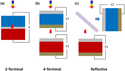
The energy losses of the single-junction solar cell originate from the unabsorbed long-wavelength photons beyond the bandgap absorption threshold, and the thermalization of excess energy in the wavelength region below the bandgap absorption threshold [Citation48]. The tandem design can better utilize the solar energy so that high-energy photons are absorbed by the upper wide bandgap subcell, while those in longer wavelength region are harnessed by the bottom narrow bandgap subcell. The configurations of tandem solar cells can be divided into a few categories and the mainstream includes the two-terminal (2-T) monolithically integrated (Figure (a)), the four-terminal mechanically stacked (Figure (b)), and the spectral splitting systems (Figure (c)). Each structure has its own advantages and constraints as well, as summarized below.
Figure 1. Three most widely studied tandem configurations (a) 2-T, (b) 4-T and (c) spectrum splitting.
The 2-T tandem solar cell uses an interconnection layer (namely a tunnelling junction or a recombination layer) to combine two subcells, and produces one open-circuit voltage (V oc, usually the sum of the V oc of the two subcells). 2-T tandems have fewer layers that parasitically absorb in the device, while it is very sensitive to the spectrum variation (morning to afternoon or different season), therefore its energy output will be limited [Citation49]. Additionally, 2-T tandems have constraints due to the stringent current matching requirement and the difficulty in fabrication compatibility between each subcell. As the current is limited by the cell with lower current, the efficiency profile shows strong sensitivity with respect to the bandgap of each subcell, making the optimum bandgap fall in in a narrow range. This renders significant difficulty for fabrication, as precise control of the compositions is required.
The 4-T tandem design has much reduced constraints, enabling easier prototyping. This is also revealed by faster progress of the 4-T perovskite tandems than that of the 2-T, as shown in the following (Figure ). Additionally, there is no need for an interconnection layer between the two subcells, which is usually a complicated part in the device as an appropriate interlayer must meet strict optical and electrical requirement (such as high transparency and conductivity). The choice for such efficient interlayer is still limited to a few types including the tunnelling junction usually employed in III-V semiconductor tandems [Citation8,50,51] and the recombination layer such as transparent conductive oxide (indium tin oxide, ITO; indium-doped zinc oxide, IZO) [Citation25,52] and thin metal films [Citation53]. Each subcell in a 4-T tandem is fabricated on a separate substrate, which therefore not only constitutes as an additional cost to the tandem system but also induces more light losses.
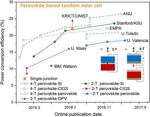
Figure 2. Efficiency evolution of tandem solar cells involving inorganic–organic metal–halide perovskites: 4-T perovskite/Si (record of 26.4% [Citation22]), 2-T perovskite/Si (record of 23.6% [Citation58]), 4-T perovskite/CIGS (record of 22.1% [Citation37]), 2-T perovskite/CIGS (record of 18.5% [Citation59]), 4-T perovskite/perovskite (record of 21.0% [Citation38]), 2-T perovskite/perovskite (record of 18.5% [Citation31]), and 2-T perovskite/organic-polymer (OPV) (record of 16% [Citation35]), and the record efficiency of the perovskite single-junction solar cell (22.1% [Citation1]).
![Figure 2. Efficiency evolution of tandem solar cells involving inorganic–organic metal–halide perovskites: 4-T perovskite/Si (record of 26.4% [Citation22]), 2-T perovskite/Si (record of 23.6% [Citation58]), 4-T perovskite/CIGS (record of 22.1% [Citation37]), 2-T perovskite/CIGS (record of 18.5% [Citation59]), 4-T perovskite/perovskite (record of 21.0% [Citation38]), 2-T perovskite/perovskite (record of 18.5% [Citation31]), and 2-T perovskite/organic-polymer (OPV) (record of 16% [Citation35]), and the record efficiency of the perovskite single-junction solar cell (22.1% [Citation1]).](/cms/asset/9bbb8514-e662-4b0c-836d-c8f85ff94d01/tsta_a_1422365_f0002_oc.gif)
Another 4-T tandem is the spectrum splitting configuration, which reflects majority of the shorter wavelength in the solar spectrum to the top cell, while efficiently transmitting the rest of the longer wavelength to the bottom cell (Figure (c)). This system also offers advantages in terms of flexibility for fabricating and optimizing the individual devices. A dichroic mirror is usually used as an optical splitter to manage the spectral reflectance and transmittance, directing the photons of different wavelengths to the most appropriate solar cell. The wavelength of the threshold of the mirror could be largely affected by the material compositions of the film used in the dichroic mirror and the placement angle. So far, this method has resulted in the highest reported efficiency for a perovskite/Si tandem of ~28%, though the efficiency is mostly contributed by the Si solar cell (20.5%) [Citation54]. The primary obstacle for the commercialization of this avenue is the need for an efficient spectrum splitter, which significantly increases the cost of the system. A modified method to avoid this obstacle is to use the perovskite cell as a reflective filter to absorb short wavelength light and reflect long-wavelength light to the bottom cell [Citation55]. However, these spectrum-splitting approaches are sensitive to the angular distribution of incoming light and would thus require a tracking system. Considering the much fewer studies compared to the other two counterparts, this structure won’t be discussed in this review.
2.2. Overview of the perovskite tandem progress
To minimize the energy loss, and in turn to maximize the PCE, the bandgap of each subcell needs to be optimized. Simulation results show that the highest efficiencies for the two-junction tandem solar cells can be reached with a bottom subcell bandgap of 0.9–1.2 eV, and a top subcell bandgap of 1.5–1.8 eV [Citation56]. In this case, a variety of narrow bandgap subcell candidates including Si, CIGS, perovskite and organic photovoltaics (OPV) are considered to be suitable. At present, the top wide bandgap perovskite subcells involve the most widely reported normal bandgap lead iodide perovskite (~1.6 eV) and the wide bandgap cell based on mixed halide (bromide/iodine, Br/I) perovskite. Combined with the versatility in the tandem configurations, there have been a number of different tandem devices reported to achieve high efficiencies. These tandems have been developed in parallel and have demonstrated very fast improvement in a short period, as shown in Figure . Among all types of tandems, the 4-T perovskite/Si tandem realizes the highest efficiency, with a value reaching up to 26.4% [Citation22]. We note that since the publication of the latest review on perovskite-based tandems on May 16 this year, there have been a number of new record efficiencies that have already emerged, such as the above-mentioned 26.4% for 4-T perovskite/Si tandem [Citation22], 21.0% for 4-T perovskite/perovskite tandem [Citation38] and 18.5% for the 2-T perovskite/perovskite tandem [Citation31]. Concurrently, the large-area perovskite-based tandem has also received much more attention leading to fast progress, e.g. a 12.96 cm2 monolithic perovskite/Si tandem cell with a steady-state efficiency of 18% has been just reported [Citation57]. Breakthroughs arrive every few months, arousing substantial interest in the PV field. The explanation for the progress of each structure will be elaborated in the following sections.
2.3. Perovskite/Si tandem solar cell
In addition to being the vast majority of the PV market, Si solar cells have a bandgap of ~1.1 eV, almost ideal to serve as the bottom subcell in a two-junction tandem structure. Perovskite/Si tandem design has been considered to be the most promising approach to commercialize the perovskite technology, as they promise a significantly higher efficiency based on an extension of the current Si cell manufacturing processes and infrastructure with relatively little modification required. Therefore, it is considered to be the least risky strategy to plan the commercialization of the perovskite technology at the present stage. Some companies are also focusing on converting the perovskite/Si tandem technology into commercial products [Citation60,61].
2.3.1. 4-T perovskite/Si tandem solar cell
Among all the tandem configurations, the 4-T perovskite/Si tandem solar cell has developed the fastest and shows the highest efficiency, as revealed by Figure . The complexity of this tandem structure mainly lies on the fabrication of semi-transparent perovskite top subcell, which is required to show both high efficiency and high transparency in the long-wavelength region to allow as many sub-bandgap photons as possible to be transmitted to the bottom cell. The first 4-T perovskite/Si yielding an efficiency of 13.4% was reported by Löper et al., which was restricted by the poor efficiency of perovskite top cell of only 6.2% coupled with a low transmittance of around 55% in the long-wavelength region [Citation36]. Shortly after this, significant progress was made with the semi-transparent subcell efficiency reaching up to 12.7% and a peak transmission at 800 nm of ~77% with Ag nanowires as the transparent contact. The overall 4-T perovskite/Si tandem efficiency, therefore, leaped to 17% [Citation24]. Compared to the opaque PSC where the contact is made of full area metal (such as gold, silver, etc.), the use of a transparent contact electrode is usually accompanied with considerable efficiency drop, originating from a series of loss channels such as high recombination rate on the interface with the hole transport material (HTM), large electrical loss due to inferior conductivity of the as-deposited film without special treatment, and also significant current loss (up to ~ 2 to 3 mAcm−2) due to a loss of a reflective rear electrode [Citation125]. Therefore, the development of the 4-T perovskite-based tandem is largely driven by the application of high-quality and efficient transparent contact materials, aside from the improvement of the perovskite film and charge selective material qualities. Chen et al. developed an ultrathin metal electrode composed of Cu/Ag, which resulted in a 16.5% semi-transparent PSC and yielded a tandem efficiency of 23.0% [Citation62]. Werner et al. further pushed the 4-T perovskite/Si tandem efficiency to 25.2% by developing In2O3:H/ITO as the transparent contact layer, before which MoOx is deposited on top of the HTM to provide physical protection from sputtering damage [Citation63]. Notably, the high efficiency delivered in this work is also ascribed to the enhanced uniformity of the electron transport layer (ETL) stack and reduced shunt paths by introducing a thin SnO2 layer between the front ITO and PEIE(polyethylenimine)/PCBM (phenyl-C61-butyric acid methyl ester) layers.
As explained above, the theoretical optimum bandgap for the top cell in a Si-based tandem is 1.7–1.8 eV [Citation39,49]. CsPbI3 has a highly suitable bandgap of 1.73 eV [Citation64], but poor phase stability is considered to be a major obstacle to make efficient CsPbI3 perovskite solar cells. The most convenient approach to tune the bandgap of perovskite is to use mixed halide (mainly I and Br) perovskites. For the inorganic perovskite CsPb(I1-xBrx)3, the bandgap can be tuned from 1.73 to 2.38 eV. The highest efficiency has been raised to 11.8% recently based on CsPbI2Br with a bandgap of ~1.92 eV, which is still far from satisfactory for highly efficient tandems [Citation65]. Similarly, the bandgap of MAPb(I1-xBrx)3 varies from ~1.57 to 2.29 eV when x increases from 0 to 1, correlating well with the change in the pseudo-cubic lattice parameter of the material. Targeting a bandgap of ~1.75 eV Pb mixed-halide perovskite with MA as cation, the atomic ratio of I to Br could be tuned to be around 1.8:1.2 [Citation66]. These materials have been widely reported to show poor photostability and thermal stability [Citation67], due to high intrinsic energetic disorder and serious phase segregation [Citation23]. In case of FAPb(I1-xBrx)3, a non-perovskite phase is formed within a range of x from 0.3 to 0.5, due to the crystal phase transition from trigonal (x ˂ 0.3) to cubic (x ˃ 0.5) structure when iodide is replaced by bromide. McMeekin et al. partially addressed this issue by employing a mixture of FA and Cs, resulting in a highly crystalline and compositionally photostable material of FA0.83Cs0.17PbI1.8Br1.2 [Citation23]. Based on a small area of 0.0919 cm−2, an impressive efficiency of ~17% has been achieved for the opaque device, and semi-transparent devices reached an efficiency of 15.1%. Correspondingly, a Si heterojunction (SHJ) solar cell with an efficiency of ~19.2% retains up to 7.3% efficiency after filtering with this wide bandgap perovskite solar cell. However, the perovskite solar cells reported in this work showed severe hysteresis behaviour in both opaque and transparent structures. This could be due to the perovskite material quality or the interface with underlying layers [Citation68–70].
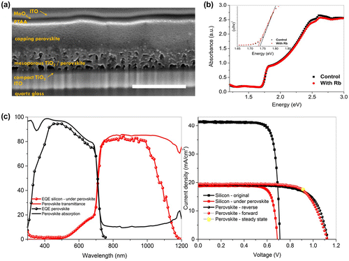
In 2017, Duong et al. developed a quadruple-cation perovskite (Cs/Rb/FA/MA) to mitigate the hysteresis and fabricated a wide bandgap (1.72 eV) perovskite solar cell with negligible hysteresis. The structure of the top perovskite solar cell can be found in Figure (a), where the mesoporous and compact TiO2 was used as the ETL and poly(triarylamine) (PTAA) was used as the hole transport layer (HTL). Incorporation of Rb into the crystals to tune the tolerance factor has been found to be the primary reason for inhibition of the hysteresis, though the fundamental mechanism is still under investigation. The stabilized efficiency of the opaque device reaches over 17% and the semi-transparent device using MoOx/ITO as the transparent contact shows an efficiency of 16.0% (Figure (c)). Due to an average transparency of over 80% in the long-wavelength region from ~700 to 1200 nm (the peak transmittance reaches 84%, Figure (c)), the Si solar cell with interdigitated back contact (IBC) after filtering demonstrates an efficiency of 10.4% from its original value of 23.9%, resulting in the record efficiency of the perovskite/Si tandem reaching up to 26.4%. With an absolute efficiency gain of 2.5% compared to the Si stand-alone device, this almost matched the record efficiency of Si single-junction device [Citation5].
Figure 3. (a) Cross-sectional scanning electron microscopy (SEM) image of the semi-transparent cell; the scale bar is 500 nm. (b) Absorption spectra of Rb-doped and Rb-free perovskite and (c) External quantum efficiency (EQE) of the semi-transparent perovskite cell and filtered silicon cell put together with the absorption and transmittance of the semi-transparent perovskite cell.
2.3.2. 2-T perovskite/Si tandem solar cell
The progress of 2-T perovskite/Si is also impressive, though the practical efficiency still lags that of the 4-T counterpart. This is understandable as the former structure strictly requires current matching and process compatibility between the two subcells. 2-T perovskite/Si tandem has been developed based on both crystalline Si homojunction and heterojunction solar cells. Notably, the former has dominated the PV industry with a global market share of approximately 93%, urging to integrate this commercially available product with high-efficiency perovskite solar cells and hence achieve low levelized electricity costs for the photovoltaic systems. In addition, the improved temperature tolerance of the c-Si bottom cell permits significantly increased flexibility in the design and fabrication of the perovskite cell. The first 2-T perovskite/Si tandem was published in early 2015 [Citation71] with an efficiency of 13.7% based on an active area of 1 cm2, constituted by a Si homojunction solar cell as the bottom subcell, a heavily doped n-type Si thin film as the interconnection layer via tunnelling effect, and an n-i-p structure perovskite top subcell. The structure has an advantage of the tolerance for high-temperature treatment (over 400 degree). However, there has been no further publication on similar structure afterwards. One of the main reasons is due to the high recombination rates existing on the p++-Si surface, as it is difficult to introduce an effective passivation layer between p++-Si and n++-Si without deteriorating the charge transfer. Very recently, great progress has been achieved based on a high-temperature tolerant homojunction c-Si bottom subcell and a mesoscopic perovskite top subcell with a tandem efficiency of 22.5% (steady-state) and a V oc of 1.75 V on a 1 cm2 cell [Citation72]. This is realized by a design of an array of metal contacts imbedded in the insulating Al2O3/SiNx passivation films on the front surface of c-Si solar cells, which enables efficient vertical charge transport for the bottom cells. This breakthrough indicates high possibility for commercialising efficient and inexpensive perovskite/c-Si tandem solar cells.
Another scheme for 2-T perovskite/Si tandem is based on Si heterojunction solar cell, which resulted in the record efficiency but can only be processed under low-temperature conditions. In late 2015, Albrecht and co-workers reported the first monolithic perovskite/Si-heterojunction tandem solar cells with an efficiency of ~18% [Citation52]. The top perovskite subcell also had an n-i-p structure, while SnO2 fabricated at low temperature was used as the ETL, enabling high efficiency of over 16% for the semi-transparent perovskite stand-alone device. ITO was used as the recombination layer that combined the two cells, which allows the completion of the Si cell with passivation and thus high voltage output of 703 mV. One month after this, Werner et al. reported efficiencies of up to 21.2 and 19.2% for tandem cells with areas of 0.17 and 1.22 cm2, respectively, partially due to the application of IZO as the recombination layer which is much more conductive than the ITO interlayer [Citation25].
In 2017, the efficiency of 2-T perovskite/Si tandem was further boosted to 23.6%, based on the device structure shown in Figure (a) [Citation58]. It combines an infrared-tuned silicon heterojunction bottom cell with the more-stable Cs/FA lead halide perovskite. This perovskite tolerates deposition of a SnO2 buffer layer via atomic layer deposition that prevents shunts, has negligible parasitic absorption, and allows for the sputtering deposition of a transparent top electrode ITO (refer to the SnO2/ZTO/ITO/LiF structure in Figure (a)). It should be noted that such a design is beneficial for thermal and environmental stability, resulting in devices that withstand a 1000-h damp heat test at 85 °C and 85% relative humidity, which is a stability landmark in perovskite technology.
Figure 4. (a) Schematic of the 2-T perovskite/silicon tandem solar cell (not to scale) with Si heterojunction solar cell as the bottom subcell. (b) Optical microscopy image of the silicon-nanoparticle (SiNP)-patterned rear side of the silicon cell before silvering. (c) Cross-sectional SEM image of the perovskite top cell, (d) the rear side of the silicon cell in an area with no silicon nanoparticles, and (e) the rear side of the silicon cell in an area with silicon nanoparticles. (f) J–V curve (NREL-certified) and efficiency at the maximum power point (inset) of the champion tandem device. (g) Total absorbance (1−R, where R is the reflectance; dashed grey line), EQE of the perovskite top cell (solid blue line), and EQE of the silicon bottom cell (solid red line).
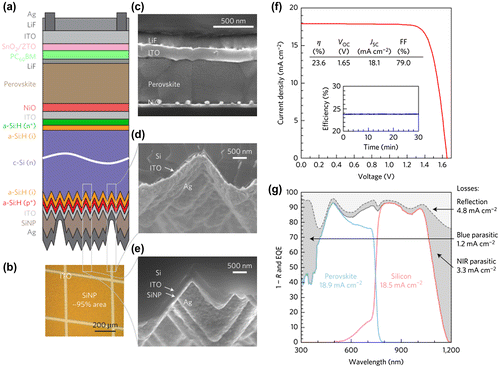
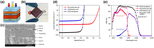
Figure 5. (a) Schematic, (b) photograph and (c) SEM micrograph of substrate configuration planar perovskite solar cells grown on a glass substrate (ZnO np represents ZnO nanoparticle). The arrows in (a) represent the illumination direction. The substrate size shown in (b) is 2.5 × 2.5 cm2. (d) J-V curves (e) and EQE spectra of the perovskite/CIGS in 4-T tandem configuration.
When fabricating the perovskite subcell in the tandem devices, especially depositing the contact materials, the vacuum-deposition processes are usually employed which increases the manufacturing cost. Therefore, developing all-solution-process is desirable and attracting. Though efforts devoted to this field are currently much fewer, an impressive efficiency has been obtained recently by Rundong Fan and colleagues who fabricate the key components in their 2-T perovskite/Si tandem solar cell, including tunnelling junction and the perovskite absorber [Citation73]. By carefully controlling the optical coupling between the top and the bottom subcells, they demonstrated an efficiency of over 20% for 2-T perovskite/Si device based on solution-processed perovskite subcells.
2.4. Perovskite/CIGS tandem solar cells
Perovskite/CIGS all-thin-film tandem solar cells have some unique advantages as they could be manufactured on thin, lightweight and flexible substrates in a cost-effective manner, therefore, offering a wide range of application opportunities, including building integrated photovoltaics (BIPV) and mobile devices. Similar to the perovskite/Si tandem, studies on the perovskite/CIGS tandem solar cell involve both the 4-T and 2-T configurations, and the former has achieved higher efficiencies. Bailie et al. firstly integrated a semi-transparent n-i-p PSC based on a silver nanowire contact with an efficiency of 12.7% and peak transmission of 77% at around 800 nm, demonstrating a perovskite/CIGS tandem with an efficiency of 18.6% [Citation24]. Subsequently, a transparent electrode based on a MoOx/Ag/MoOx dielectric/metal/dielectric structure was developed by Yang’s group and applied in an n-i-p PSC leading to an efficiency of 12.4%, though lower infrared transmission (less than 70% on average) resulted in a poorer efficiency of ~15% for the tandem device [Citation74]. Guchhait et al. then dramatically improved the semi-transparent n-i-p PSC efficiency to 16% by employing a Ag/ITO transparent contact and achieved a tandem efficiency of 20.7%, which, however, suffered from a low average transparency of 54% from 800 to 1400 nm [Citation29]. The recently reported highest efficiency for the 4-T perovskite/CIGS tandem is 22.1%, contributed by a 16.1% p-i-n structure PSC and high average transmittance of 80.4% between 800 and 1200 nm. This still has not surpassed the record efficiency of 22.6% for the single-junction CIGS [Citation37]. A flexible perovskite/CIGS tandmem solar cell has also been demonstrated recently by Stefano Pisoni and colleagues, with an efficiency reaching up to 18.2% and a high average transmittance of 78% between 800 and 1000 nm [Citation75]. This impressive photovoltaic performance is of great importance, as such a device configuration is highly compatible with the roll-to-roll manufacturing.
The development of 2-T perovskite/CIGS tandems encounters similar complexities with 2-T perovskite/Si tandem due to the constraints originating from the 2-T design. It has an additional challenge because the conventional CIGS with a structure of substrate/Mo/CIGS/CdS/transparent contact requires a perovskite top cell with a p-i-n structure. P-i-n PSC usually induces inferior V oc and current density due to severe recombination at the contact/perovskite interface compared to the n-i-p structure [Citation58]. This is also evident by the fact that the majority of the single-junction PSCs reported with the highest efficiencies are based on the latter structure [Citation18,76,77]. Todorov and co-workers reported a 10.9% 2-T perovskite/CIGS tandem solar cell for the first time in 2015, in which each cell was customized for monolithic integration in the following sequence: transparent conducting electrode/PCBM/perovskite/poly(3,4-ethylenedioxythiophene) polystyrene sulfonate (PEDOT:PSS)/ITO/CdS/CIGS/Mo/Si3N4/glass [Citation27]. The bottom CIGS absorber has a bandgap of ~1.04 eV for improving the photon management in the long-wavelength region (extending to over 1200 nm). Bandgap tuning for the top perovskite solar cell was comprehensively carried out for better current matching. With better understanding about materials, especially wide-bandgap materials, along with more advanced techniques for fabricating a semitransparent device, the 2-T perovskite/CIGS can reach higher efficiency. Uhl et al. recently projected an efficiency of 18.5% for 2-T perovskite/CIGS by using a highly efficient semi-transparent p-i-n PSC with C60/bis-C60/ITO as the ETL and perovskite with optimized bandgap to match the CIGS solar cell [Citation59]. We note that the efficiency was projected by measuring the perovskite and CIGS solar cell separately rather than from a complete monolithic cell.
2.5. Perovskite-perovskite tandem
An ‘all-perovskite tandem’ design is an attractive solution to advance solar cell efficiency beyond the S–Q limit, while preserving the low-cost advantages of perovskites [Citation30]. The best wide bandgap perovskites to date are based on the lead Br/I mixtures, which have undergone intense investigation especially for fabricating highly efficient perovskite/Si tandem solar cell and achieved relatively satisfactory efficiencies of ~17% with ~1.75 eV bandgap [Citation22,23]. Therefore, fabrication of efficient perovskite/perovskite tandem solar cells largely depends on the development of narrow-bandgap perovskites.
Substituting Pb with Sn to form a Pb-free material can extend the absorption range to over 1000 nm [Citation16] and pontentially yield a narrow-bandgap perovskite. With an initial efficiency of less than 5.8% reported in 2014, Noel et al. achieved similar efficiency of 6.4% using MASnI3 with Cl doping in the same year [Citation78]. Nevertheless, Sn2+ in the perovskite is easily oxidized to Sn4+ by less than 0.1% O2 [Citation79]. Sn4+ can heavily dope the material and degrade the solar cell performance, and the as-prepared device is extremely unstable [Citation80]. The addition of SnF2 decreases the tin vacancy concentration by filling up the degenerate energy levels, and improves the photovoltaic performance [Citation81]. Other strategies such as solvent-engineering have also been found to be beneficial for controlling the crystallization process for the pure Sn-based perovskite and producing more efficient solar cells [Citation82]. Despite this, the efficiency for the solar cells based on pure-Sn perovskite has almost stagnated over the past three years.
A breakthrough was made in 2016 on the narrow bandgap absorber by forming the Sn/Pb binary perovskite, which has a tuneable bandgap spanning from ~1.15 to ~1.5 eV. The minimum bandgap of the Sn/Pb binary perovskite is even lower than that of the pure-Sn perovskite, thanks to the anomalous bandgap bowing effect (namely lack of conformity with Vegard’s law) [Citation30]. Zhao et al. systematically studied the correlation between the structural and photophysical properties of MA(PbxSn1-x)I3 [0 ≤ x ≤ 1] perovskites by substituting Sn with Pb [Citation83]. The 60% and 80% Sn content materials have bandgaps of ≈1.27 and 1.19 eV, respectively. It is notable that the minimum bandgap of Sn/Pb binary perovskite also falls in the region that is predicted to have the highest efficiency as the bottom subcell of the two-junction tandem. In addition, devices based on the Sn/Pb binary perovskite materials also exhibit much better PV performance and stability than those based on pure Sn perovskites. A Pb-assisted two-step method was proposed by Li and co-workers to fabricate high-quality MASn0.5Pb0.5I3 perovskite film, which showed regular crystalline grains with a flat and compact morphology as well as full coverage on the planar PEDOT:PSS substrate [Citation84]. The corresponding devices showed a remarkable PCE of 13.6% with high reproducibility. Liu et al. fabricated PSCs based on uniform MAPb0.75Sn0.25I3 (bandgap of ~1.3 eV) film by the solvent-engineering approach and consequently realized a PCE of 14.12% [Citation85]. Liao et al. innovatively used the precursors combining FASnI3 and MAPbI3 and pushed the efficiency of over 15% with a composition of (FASnI3)0.6(MAPbI3)0.4 absorber with an absorption edge of ∼1.2 eV [Citation86]. Recently, the same group realized a record efficiency of 17.5% with the same composition and similar device structure but optimizing the perovskite thickness as well as improving the carrier lifetimes via film crystallinity, which effectively enhanced the EQE in the IR wavelength range of 700 to over 1000 nm [Citation38].
Due to the independence between the subcells in a 4-T tandem, any improvement achieved for either subcell will result in enhancement in the 4-T tandem efficiency. Thus, the abovementioned record efficiency for the Sn/Pb binary perovskite single-junction device also resulted in a record efficiency of 21% for the 4-T perovskite/perovskite tandem [Citation38]. It should be pointed out that an appropriate bandgap for the bottom subcell is also necessary to guarantee the high efficiency for tandem, which was 1.25 eV in this work (Figure ).
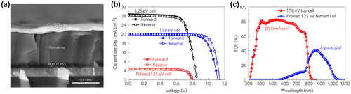
Figure 6. (a) Cross-sectional SEM image of a PSC with a 620 nm-thick (FASnI3)0.6(MAPbI3)0.4 absorber. (b) J–V curves of the semi-transparent wide-bandgap (1.58 eV) PSC under glass/FTO illumination and the narrow-bandgap (1.25 eV) PSC with and without the semi-transparent wide-bandgap PSC optical filter. (c) EQE spectra of semi-transparent wide-bandgap (1.58 eV) PSC top cell and filtered narrow-bandgap (1.25 eV) PSC bottom cell. The integrated J sc over a 100 mWcm−2 AM1.5G solar spectrum for the 1.58 eV top cell and the filtered 1.25 eV bottom cell is 20.0 and 4.8 mAcm−2, respectively.
As the perovskite material cannot withstand high temperature treatment, any material involved in the perovskite/perovskite tandem must be deposited at low temperature. This makes many of the efficient charge transport materials that lead to high efficiency PSC unsuitable. However, the low fabrication temperature makes the device compatible with a wide range of substrates, including flexible substrates and textiles. Forgács et al. fabricated a 2-T perovskite–perovskite tandem using the vacuum deposition method, and achieved an efficiency of 18% [Citation33]. There is still substantial space for improving this efficiency, as the combination of bandgaps of the two subcells (top cell bandgap of 2.0 eV and the bottom bandgap of ~1.6 eV) is non-ideal. Eperon et al. circumvented this issue by using a 1.8 eV top subcell and a 1.2 eV bottom subcell, and achieved 17%-efficient 2-T perovskite/perovskite tandem using solution processing [Citation30]. Recently, the record efficiency has reached 18.5% for the 2-T perovskite/perovskite tandem solar cell by Rajagopal and co-workers, after cautious control of the bandgap and film thickness of each subcell to approach current matching (Figure ). Notably, a high V oc of 0.84 V was achieved for a small bandgap of ~1.2 eV, by using a fullerene variant, indene-C60 bis-adduct, which facilitates higher quasi-Fermi level splitting, reduces non-radiative recombination, and alleviates hysteresis instabilities. Correspondingly, a high V oc of 1.98 V (approaching 80% of the theoretical limit) was obtained for the as-prepared 2-T perovskite/perovskite tandem, which is much superior compared to that of 2-T perovskite/Si tandem which was reported to be in the range of 1.7–1.8 eV [Citation25,52,58]. The current and FF are the main parameters that require greater improvement for 2-T perovskite/perovskite tandem, which rely on further development of the narrow bandgap perovskite subcell.
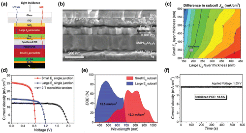
Figure 7. (a) Device structure and (b) cross-sectional SEM image of a characteristic device. (c) Corresponding difference in subcell photocurrent (J ph,f − J ph,b), where contour line representing J ph,f − J ph,b = 0 (ideal current matching) is highlighted and region corresponding to thickness combination used in this work (190 ± 10 nm and 350 ± 10 nm) is marked. (d) Typical J–V characteristics of 2-terminal tandem solar cell along with that of the small- and large-bandgap single-junction solar cells with Ag electrode. (e) EQE spectra of individual subcells in 2-T monolithic tandem. (f) Steady-state current under AM1.5 illumination at an applied voltage corresponding to maximum power point (MPP) of tandem solar cells.
3. Large-scale device design
The ultimate application of perovskite solar cells either in single-junction or tandem configuration relies on the scalability of the perovskite technology. However, the majority of the abovementioned record efficiencies are based on devices with an active size generally in the range of 0.1–0.3 cm2. The large area was usually around 1 cm2, far away from the 6-inch size usually used for Si solar cell and the m2 scale required for modules. Scaling up the perovskite technology and maintaining high efficiency over large areas will lead to challenges including how to deposit large-area perovskite thin films with high uniformity, how to improve the reproducibility of cells and how to reduce electrical losses by designing the interconnection of single cells to make large modules.
3.1. Efficient large-scale perovskite devices
A simple way to deposit perovskite film in the laboratory is spin-coating the precursor with the help of an anti-solvent to control the crystallization process. However, this method is unfavourable for scaling up because it not only tends to produce non-uniform large-area films, but also wastes a lot of perovskite solution and is very sensitive to many technical conditions such as humidity, vapour pressure and the anti-solvent dropping time [Citation87]. Some other industry friendly deposition techniques have been exploited, including vacuum flash [Citation88], hot-casting [Citation89], blade coating [Citation90–95], spray-coating [Citation96–99], slot-die coating technologies [Citation100,101] and pressure-assisted process [Citation102], bridging the gap between academic research and its industrial counterpart. In the following, a few important breakthroughs made for large-scale perovskite deposition with different fabrication methods will be introduced.
The vacuum-flash solution process consists of two stages, with the precursor solution spin-coating followed by applying a vacuum-flash treatment to enable a sudden and well-controlled removal of solvent [Citation88,103,104]. This treatment is, therefore, able to boost the rapid crystallization of the perovskite precursor phase. Li and co-workers fabricated PSCs using this method with an aperture area exceeding 1 cm2 and optimized a series of fabrication conditions including the vacuum pressure and the composition. Eventually, they demonstrated a maximum efficiency of 20.5% and a certified PCE of 19.6% over a 1 cm2 device [Citation88]. Ding et al. also achieved efficiency up to 19.0% with a large area of 1.13 cm2 by employing the same method [Citation103]. Notably, they also found that high-quality perovskite films can be prepared using this method in air with a relative humidity of 45−55%.
Hot-casting process is performed by coating the perovskite solution on a pre-heated substrate, which can facilitate the film formation and crystallization. In 2015, Nie et al. first raised the idea to use the hot-casting process to prepare continuous and pinhole-free perovskite film [Citation105]. They fabricated planar devices with small area, which showed an efficiency approaching 18% with high reproducibility and hysteresis-free photovoltaic response. This method produced large, millimetre-scale, perovskite grains which have reduced bulk defects and improved charge carrier mobility. Liao et al. further employed this method to fabricate large-scale perovskite solar cells by incorporating Cl− in the crystal, and obtained 15.4% for a 1 cm2 device and 12% for a module with an area of 5 cm × 5 cm [Citation89]. A drawback of both methods mentioned above is that they still involve a spin-coating step, which cannot be used for making highly efficient large-scale (m2) devices.
Blading-coating, another solution-based method, does not have the above constraint. This method includes spreading the solution on the substrate with a blade, followed by post-treatment. Razza et al. fabricated perovskite using sequential step deposition, where the PbI2 film was deposited using blade coating and then dipped in a MAI solution [Citation93]. A module efficiency of 10.4% was obtained for a 10.1 cm2 active area, and an efficiency of 4.3% was measured for a module area of 100 cm2. Meanwhile, blade coating of perovskite films in air was developed by Kim and co-workers with a respectable efficiency of ~10%. Importantly, it was also found that the as-prepared device showed much better stability under ambient conditions [Citation92]. Tang et al. carried out compositional engineering of doctor-bladed PSC by incorporating a small amount of Cs+ and Br− ions into perovskite precursor solution, which reduced the required film formation temperature. Pinhole-free perovskite thin films with micrometer-sized grains have been obtained with the assistance of secondary grain growth with MACl added into the precursor solution. PSC using these blade-coated thin films achieved a highest stabilized PCE of 19.3%, albeit for a small area device. Nevertheless, this represents a significant step toward scalable manufacture of PSC [Citation91].
Using an ultrasonic spray-coating method, Barrows et al. made a first optimization of processing parameters (including temperature of the substrate, the volatility of the casting solvent and the post deposition anneal) under ambient conditions for the fabrication of planar MAPbI3 perovskite solar cells [Citation97]. With the creation of dense perovskite films, PCE of up to 11% was realized. Tait and co-workers showed the versatility of concurrently pumped ultrasonic spray coating by rapidly and precisely optimizing precursor ratios to achieve highly crystalline and pinhole-free layers, and fabricated the first perovskite solar modules (3.8 cm2) with an efficiency of 11.7% [Citation98]. Recently, a certified efficiency of 12.1% for a 16 cm2 module was achieved with this method by optimizing the key parameter, namely the spraying pressure [Citation96]. These results demonstrate that spray-coating can be used in the large-area and low-cost manufacture of high efficiency PSC.
A novel deposition route for the large-scale perovskite films that has been recently developed is worth mentioning, as it does not rely on the use of a common solvent or vacuum process [Citation102]. Instead, it relies on the rapid conversion of amine complex precursors to perovskite films, followed by a pressure application step. The detailed process can be found in Figure . Using this method, a module with an aperture area of 6.0 cm × 6.0 cm was fabricated with a certified efficiency of 12.1% (I sc of 73.0 mA, V oc of 8.36 V, and FF of 0.715) on an area of 36.1 cm2. This method opens up a new solvent- and vacuum-free approach to the production of uniform thin perovskite films in large scale, and holds substantial potential for propelling the production of perovskite modules and its application in the perovskite tandem modules.
Figure 8. (a) The steps of the pressure processing method: (I) add amine complex precursors and cover with polyimide (PI) film; (II) apply pressure; and (III) heat and peel off the PI film. (b) SEM images and (c) X-ray diffraction patterns of the perovskite film converted from amine complex precursors via the pressure processing method (the present technique), in comparison with images and patterns from a reference sample that was deposited by the spin-coating method with a post-treatment by CH3NH2 gas.
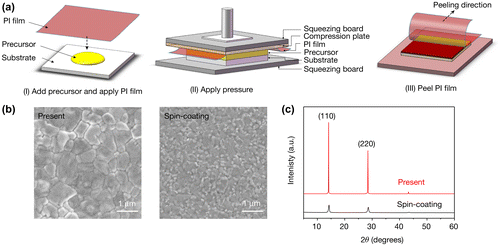
Figure 9. (a) Schematic of the 4-T perovskite/c-Si multi-junction photovoltaic devices in module-on-cell architecture. J-V characteristics of the optimized (b) perovskite top solar module with seven subcells stacked on top of (c) an IBC c-Si bottom solar cell.
3.2. Module design for perovskite device
To circumvent the quadratic scaling of series resistance with the cell width, one method is to physically isolate the large area device into thin strips followed by series connection [Citation106]. Isolation, which requires highly precise alignment to minimize ‘dead-area’ losses, could be achieved by laser ablation, physical scribing, or chemical etching and metal deposition [Citation107] Laser ablation has been successfully developed to fabricate highly efficient perovskite modules, with the structure of a standard P1, P2 and P3 approach [Citation107]. P1 scribe lines form the front contact isolation between cells, and P2 lines form the interconnection between the front contact and the subsequently deposited back contact. P3 lines remove the back contact and the light absorber to isolate the back contact of the cells, leading to completed series interconnection. Moon et al. used laser-scribing techniques to pattern the module segment, reduce the dead area, and optimize the aperture area efficiency. A small fraction of the dead area in the module (less than 16%) has been achieved, which proves that the laser-scribing technology can be adopted for monolithic serial interconnected perovskite modules. Mini-modules with an area of 5 × 5 cm2 were fabricated with an efficiency of ~6% [Citation107]. Simulation studies reveal that the optimum width of the subcell in the module strongly depends on the sheet resistance of the TCO [Citation108]. With the same laser patterning method combined with passivation using graphene and related two-dimensional materials at the perovskite/m-TiO2 interface, perovskite solar modules with an active area 50.6 cm2 achieved a record PCE of 12.6% [Citation106].
An alternative means to realize efficient large-area cells is to employ metallic grid lines to increase the effective conductivity of the transparent contact electrode. This design reduces the complexity of the fabrication process. Hambsch et al. utilized simple Al grid lines to increase the conductivity of the transparent electrode with the same structure inherited from their design in OPV [Citation109], achieving an efficiency of 6.8% for a PSC with an aperture area of 25 cm2 without relying on an interconnected strip design [Citation110]. These grid lines were exposed to UV-ozone plasma to grow a thin Al2O3 layer, which dramatically improves the wetting and perovskite film formation on top of the lines and reduces the probability of short circuits between the grid and the top electrode. Kim et al. incorporated the same configuration in a large-area 16 cm2 cell, demonstrating a certified efficiency of 12.1% [Citation96].
3.3. Progress of tandem mini-module
In order to make perovskite-based multi-junction devices scalable to large areas, the area of the semi-transparent perovskite top cell needs to be increased, which thus requires the transparent contact layer to be very conductive. However, the trade-off between sheet resistance and optical transparency of the transparent conductive electrode creates challenges for designing large-area semitransparent cells.
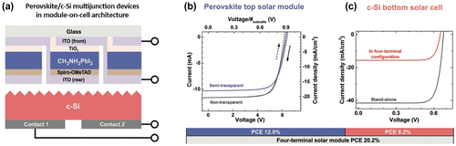
A module-on-cell concept where a perovskite solar module with interconnected subcells is combined with a Si solar cell has been demonstrated to fabricate 4-T multi-junction solar modules by Jaysankar and co-workers [Citation111]. They investigated the impact of transparent rear electrode thickness by performing a detailed optoelectronic analysis and then optimized the perovskite solar module design for maximal performance. The highest tandem efficiency for a perovskite/Si tandem mini-module is 20.2% with an active area of 4 cm2. In a recent conference presentation, the same group has presented an efficiency of over 23% for the tandem module with the same area of 4 cm2 [Citation112]. Concurrently, a 12.96 cm2 monolithic tandem cell with a steady-state efficiency of 18% has been recently reported thanks to the employment of an improved recombination junction based on nanocrystalline silicon layers [Citation57]. This layer not only reduces the reflectance and absorption losses compared to the widely used TCO recombination layer, but also has low lateral conductivity enabling the upscaling of monolithic perovskite/Si tandem cells with minimum electrical losses.
A scalable thin-film 4-T perovskite/CIGS photovoltaic module with an area of 3.76 cm2 has been presented by Paetzold et al. with a power conversion efficiency of 17.8% [Citation113]. Their prototype outperforms both the record single-junction perovskite solar module of the same area as well as the reference CIGS solar module. Both submodules apply a scalable interconnection scheme that can accommodate scale-up towards square meter scale thin film multi-junction solar modules. It is evident that development of highly performing perovskite-based tandem modules is an important theme that requires more attention in the years to come.
4. Guidelines for improving the tandem efficiencies
Tandems involving perovskite have undergone a meteoric rise since the first report around three years ago [Citation36]. Though it is too early to predict when the theoretical-proven efficiency of 30% could be reached, there have been a few directions that clearly need more intensive study as indicated from experimental reports and detailed optical simulations.
4.1. Highly efficient transparent conductive layer
In all tandem configurations, a key element is an efficient transparent conductive contact material. A range of candidates, including various transparent conducting oxides (TCOs), ultrathin metal layers, silver nanowires (AgNWs), and graphene, have been exploited. TCOs have been the most widely used transparent contact materials, in the cases of both front and rear contacts. TCOs also have a long developing history as a requirement in many other optoelectronic applications [Citation114]. A myriad of TCO candidates including ITO [Citation22,23,36,52,58,115], In2O3:H/ITO [Citation25], IZO, ZnO:Al [Citation26,37], and In2O3:H [Citation26] have been applied in tandems involving perovskite, and all led to impressive efficiencies in different tandem configurations. For instance, both of the record efficiencies of 2-T [Citation58] and 4-T [Citation22] perovskite/Si tandem at the moment are realized using ITO transparent layer as the front contact. TCOs are normally deposited by sputtering, which require meticulous control over the deposition parameters, especially the deposition power and the associated atmosphere pressure. To more completely alleviate the damage caused by the ion bombardment, a protective interlayer, such as MoOx or WOx, is required [Citation116]. However, introduction of these layers induces light loss due to strong absorption. They also raise concerns about the long-term stability by not only being easily oxidized in air, but also reacting with iodine diffusing from the perovskite absorber [Citation117]. Therefore, it is vital to explore more stable and efficient buffer layers. Alternatively, another promising strategy is to deposit inorganic charge transport layers before sputtering the TCOs, which has the potential to mitigate the necessity for the buffer layer. A successful example is the 2-T perovskite/Si tandem with p-i-n perovskite top cell, where a bilayer of SnO2 and zinc tin oxide (ZTO) was introduced to protect the underlying PCBM organic layer before sputtering ITO [Citation58]. Besides the benefit of robustness towards sputtering, this method is also capable of improving the device stability, and therefore is a promising direction for constructing highly efficient and stable semi-transparent perovskite solar cells.
AgNWs display high transmittance from 300 to 1200 nm and achieve excellent conductivity <20 Ωsq−1. Efforts have been devoted to spin-coating [Citation118] or spraying [Citation28] AgNWs onto the surface of the charge transport material, but this usually deteriorates the underlying layers by using unfavourable solvents. Instead, they could be deposited on a separate flexible substrate first and then transferred to the PSC [Citation24]. Intrinsically, AgNWs are not an ideal candidate as they cause poor stability in PSC mainly attributed to chemical reactions between the sublimed I and Ag. The as-formed AgI layer is insulating, and thereby increases the sheet resistance and impairs the charge extraction.
Graphene shows exceptional promise as a transparent conductive material, as it demonstrates excellent (90%) transmittance across the whole solar spectrum with little free carrier absorption [Citation119]. However, graphene is typically grown at high temperatures (~1000 °C), and is therefore usually independently fabricated first and then mechanically transferred onto the PSC. Similar to AgNWs, the transfer process is rather complicated and the success rate is usually low. In addition, graphene usually has high native sheet resistance usually in the several hundreds of Ωsq−1. Such issue can be addressed using metallisation with a grid of narrow metal lines, similar to that used for the TCOs.
Ultrathin metal layers with a thickness of usually less than 10 nm have also been used as alternative transparent electrodes, which can be deposited by thermal evaporation and thus do not require buffer layers to protect the underlying layer [Citation62,74,118]. Though the metal-based electrodes have very high conductivity that can reduce the electrical loss, the optical loss is usually significant, especially in the infrared region. Chen et al. fabricated a semitransparent electrode of Cu (1 nm) and Au (7 nm) with an additional layer of bathocuproine (BCP) to further improve the transmittance of the electrode, but transmission was still limited to 60% in the infrared region [Citation62]. Thus, ultra-thin metal layers are not considered to be the best transparent contact candidate.
4.2. Efficient and stable wide bandgap perovskite as top subcell
An efficient wide bandgap perovskite top subcell is required for any type of tandem. In terms of this, attention has now shifted away from single-cation perovskites to multi-cation, in cases of both normal bandgap and wide bandgap. This also seems to be a promising approach that can dramatically improve the device stability [Citation22,23]. However, the quality of the wide bandgap perovskite is still far away from satisfactory. The highest reported V oc till now for the bandgap in this region is 1.2 V vs. a bandgap of 1.75 eV, indicating a V oc deficit as high as 0.55 V. This is considerably higher than 0.38 V for the normal bandgap perovskite (1.62 eV) [Citation76] and 0.4 V for the narrow bandgap Sn/Pb binary perovskite [Citation38]. Reduction of V oc loss-in-potential for wide-bandgap perovskites is particularly crucial, and it is also important from other perspectives, as this is the major parameter preventing PSCs from reaching their thermodynamic limit. Specific efforts should be devoted to further optimizing the perovskite composition and deposition process to reduce the inherent disorder, and develop more efficient charge transport materials (targeting for better aligned energy levels [Citation120,121], high charge transport efficiency, low optical loss), and interfacial passivation [Citation122].
Wide bandgap perovskite suffers from similar degradation issues to the normal bandgap perovskite, such as moisture attack on the organic species in the molecule, and bias-induced ion migration. Additionally, wide bandgap perovskite has been widely reported to show a light-induced phase segregation. For instance, for MAPb(I1-xBrx)3, the luminescence peak of the perovskite material is red-shifted to 1.68 eV under illumination in less than 5 min, regardless of the halide composition and the original bandgap with 0.2 ˂ x ˂ 1 [Citation67]. Concurrently, growth in sub-bandgap absorption states and splitting of the X-ray diffraction peaks were also observed. Interestingly, such phenomena seem to be largely reversible as the original luminescence peak can be recovered after storing the device in the dark. The luminescence peaks observed after photoexcitation-induced splitting have been ascribed to iodide-rich and bromide-rich regions that result from halide segregation [Citation123]. Light-induced phase segregation depends on the electron–phonon coupling and defect concentration in the material through vacancy-mediated halide migration [Citation23]. Recently, it was also found that the magnitude of the phase segregation depends on the operating condition of the solar cell [Citation124]. Under short-circuit and maximum power point conditions, phase segregation is almost negligible compared to the magnitude of segregation under open-circuit conditions, in the case of quadruple cation perovskite. This emphasizes the fact that tuning the perovskite composition, such as using the multiple cation strategy, has the potential to significantly supress the light-induced phase segregation by lowering the electron-phonon coupling and the defect density. In addition, growing larger perovskite crystals with lower defect concentration has been shown to bring the same benefit [Citation125].
4.3. Efficient narrow bandgap PSC for perovskite-perovskite tandem
Perovskite/perovskite tandem efficiency is limited by the unsatisfactory efficiency of the narrow bandgap bottom subcell. More generally, studies on perovskites with bandgap somewhat lower than the extensively investigated MAPbI3 would also be beneficial for constructing the highest single-junction cell. Similar to pure-Pb based perovskite, relatively low loss-in-potential (~0.4 V) has been achieved for the narrow-bandgap Sn/Pb binary perovskite solar cells, with V oc up to 0.85 V vs. a bandgap of ~1.25 eV [Citation38]. In contrast to the pure Pb perovskites which have already resulted in quantum efficiencies approaching 100%, Sn/Pb binary PSCs currently achieve much lower maximum quantum yields of ~80% in the wavelength region of ~400 – 700 nm and ~70% in the long-wavelength region (~700–1000 nm). Correspondingly, the J sc yield of ~28 mAcm−2 is substantially lower than its S–Q value of 41 mAcm−2 [Citation38]. The especially low-quantum efficiency in the long-wavelength region is primarily due to insufficient absorption caused by the utilization of relatively thin (~400 nm) Sn/Pb binary perovskite layers. Due to the short carrier lifetime (<20 ns) of Sn/Pb perovskite materials, thick Sn/Pb perovskite layers will readily lead to large carrier recombination rates. Therefore, to produce thicker mixed Sn/Pb perovskite thin films with enhanced carrier lifetimes is important to further enhance the J sc of the as-prepared device, and to fabricate high-quality Sn/Pb binary perovskite by controlling the deposition process will be essential [Citation38].
Improved carrier selective contact materials are also required for the Sn/Pb binary perovskite solar cell. This is revealed by the poor FF of ~0.7 (well below the S–Q limit of 0.87), which is affected by unwanted bulk and interfacial carrier recombination, parasitic resistance and other electrical non-idealities. Until now, most of the contact materials, both ETMs and HTMs, are straightforwardly inherited from pure Pb-based perovskite, and are not well suited to the Sn/Pb binary perovskite. For the ETL, either high-temperature-processed TiO2, which is not compatible for perovskite/perovskite tandem due to the decomposition of the perovskite, or organic transport materials that show low mobility have been reported. For the HTL, low mobility organic materials have been used which again limit the charge extraction efficiency and show poor stability. More crucially, these HTLs usually contain lithium and/or cobalt salt doping to improve the electrical properties of the HTL which can easily damage the Sn perovskite and lead to deterioration of the stability of PSC [Citation16]. Dedicated efforts devoted to this direction are therefore crucial.
4.4. Interconnection layer for 2-T tandem solar cell
In current-matched monolithic tandem solar cells, the hole current from one subcell and the electron current from the other subcell must recombine with high efficiency and minimal loss of electrical potential in a suitably designed interlayer. In the widely explored III-V semiconductor tandem, a tunnel junction is usually applied as an efficient interlayer [Citation19]. In the tunnel junction, degenerately doped p++ and n++ materials produce a thin junction in which the valence band on the p-side is energetically aligned with the conduction band on the n-side, and the depletion region is sufficiently thin that carriers can tunnel from one side to the other. Meanwhile, in OPVs, recombination layers are incorporated, including thin film metal and transparent conductive layers. So far only established materials that have been used in other tandems have been incorporated in tandems involving perovskites, while little study on exploring new and efficient interconnection layers has been carried out. One progress that is worth mentioning is based on the work by Sahli et al. recently, where they employed an improved recombination junction based on nanocrystalline silicon layers. This design has been proven to be efficient in reducing reflection and parasitic absorption losses in comparison to a commonly used TCO recombination layer [Citation57]. When employed in monolithic perovskite/silicon heterojunction tandem cells with a planar front side, this junction is found to increase the bottom cell photocurrent by more than 1 mA cm−2. It needs to be emphasized that development of efficient interlayer is of great importance, as it can both optically and electrically affect the ultimate device performance [Citation126]. Aside from this, when considering the fabrication compatibility between the two subcells, the morphology and the physical/chemical properties are rather important, e.g. depending on the tandem system it may be highly desirable that the interconnection layer can prohibit the potential issues such as the solvent penetration or be tolerant of high temperature treatment.
4.5. Reducing optical loss
To make best use of the solar spectrum with the tandem configuration, the bandgap of each subcell needs to be matched so that the current in each subcell is the same. Practically, the absorption in each subcell is largely dependent on the perovskite absorber thickness. Therefore, to reach the maximum efficiency, the absorber thickness should be carefully controlled, for which there have been many optical simulations that can serve as useful references [Citation19,127,128]. Another significant optical loss comes from parasitic absorption in the charge transport layer. In Grant’s simulation of the detailed optical loss for the monolithic perovskite/Si tandem, Spiro-OMeTAD, the most extensively employed HTL in n-i-p PSC, results in a great deal of parasitic absorption. The corresponding current loss, depending on the device structure, could reach ~2 mAcm−2 [Citation129]. It would be beneficial to replace Spiro-OMeTAD with a hole transport material having a high reflection index, such as NiOx. Aside from the abovementioned two optical losses, reflection loss is also significant, which is a well-recognized issue in many other solar cell configurations. Anti-reflection layers have proven to be effective in reducing such loss, such as MgF2 [Citation22] and LiF [Citation58], usually used at the air/glass and air/TCO interfaces. Decorating the front electrode of the top cell with some textured films is also efficient and successfully used in a few highly efficient tandems [Citation22,52]. More emphasis needs to be placed on the optical simulations as they are very helpful for the experimentalists to design the structure; they target at proper materials, and optimize the optical parameters in a correct and more efficient approach. More detailed explanation and discussion about the optical simulation on perovskite based tandem device has been included in a previous review by Junnan Hu and et al. [Citation130], therefore this topic will not be discussed more here.
5. Challenges that lie ahead
For further enhancing the commercial competiveness of the perovskite tandem, the near-term target would be to increase the efficiency beyond 30%. Other major challenges for commercializing this technology include not only the abovementioned scaling up of devices to module size, but also improving the operational lifetime to 25 years, and establishing processing approaches for reducing the toxicity during handling of Pb or other relevant metals, and the use of hazardous solvents.
5.1. Stability
The stability of the perovskite solar cell, which will translate directly to the stability of the tandem module, has become one of the stumbling blocks preventing perovskite technology from becoming ready for large-scale application. Instability induced by moisture has been first noticed and given most concern, as moisture can readily react with the perovskite and result in chemical degradation. Afterwards, perovskite materials have been further found to be susceptible to many other conditions including heat [Citation131], prolonged UV irradiation [Citation132], visible light irradiation [Citation124,133], environment (such as oxygen) and electrical bias [Citation134] as a consequence of their low formation energy. Notably, compared to the other conditions, studies exploring the influence of oxygen on perovskite device performance are much fewer, and these have only covered the widely used simple composition MAPbI3 [Citation134–137]. This requires particular attention, as Bryant and co-workers have found that light and oxygen induced degradation occur even faster than the more widely studied moisture induced degradation [Citation134]. Aristidou et al. explained that photoexcited electrons in the perovskite layer interact with oxygen molecules to form superoxide (O2 −) and break down the perovskite through deprotonation of the MA cation [Citation138], while Zhang and Sit claimed that superoxide attacks the perovskite by reacting with a surface Pb ion and ultimately results in a local PbO structure [Citation137]. The above listed so-called extrinsic factors that activate several degradation mechanisms can be alleviated by encapsulation to isolate the device from these external sources of degradation. Very encouraging progress is that a standard industrial encapsulation process has enabled perovskite devices that withstand a 1000-h damp heat test at 85 °C and 85% relative humidity [Citation58].
A more alarming issue that has been reported for single-junction perovskite solar cells is intrinsic degradation. For instance, gold, which has been used as the contact for the majority of opaque PSC, has been found to be mobile and can penetrate to the perovskite layer leading to damage [Citation139]. Luckily, this would not be a significant issue for tandems, as usually the semi-transparent devices either don’t use Au, or have a transparent contact as a buffer layer [Citation58]. Another source of intrinsic degradation is that organic HTMs such as Spiro-MeOTAD and PTAA usually contain lithium ions that can readily migrate and deteriorate the underlying perovskite film [Citation140]. This can be adequately mitigated by using an efficient inorganic hole conductor, such as CuSCN [Citation141] or NiOx [Citation142]. Mesoporous devices incorporating carbon electrodes are found to be very stable, though the efficiency has not caught up with the others [Citation143]. A series of recent reviews have summarized the degradation mechanisms of the intrinsic and extrinsic stability of PSCs within different structures and materials and have provided some strategies for improving device stability [Citation144–147]. Overall, degradation can be alleviated by altering material composition, device structures and interfaces [Citation148]. This is an essential step in the perovskite tandem research that requires substantial further work.
5.2. Toxicity
The toxicity issue associated with the Pb content in the most highly performing perovskite solar cells has been widely recognized by the research community [Citation45,149,150]. The toxicity related to heavy metals has been met before for CdTe PV, which is hazardous to human health as well as contaminating the environment. Currently, CdTe technology has succeeded to enter the PV market thanks to the development of cost-effective and environmentally friendly recycling programmes. However, PSCs encounter a much more severe issue as they can easily degrade to Pb with a K sp (Solubility product constant) up to 29 orders of magnitude higher than CdTe [Citation151]. Sn has been proposed as a more environmentally friendly alternative to Pb. Yet toxicological assessment clearly shows that a Sn based perovskite may not be the ideal Pb surrogate to mitigate the toxicity issue, as it can likewise induce detrimental environmental and health effects due to reduced pH value rather than the presence of the heavy metal [Citation149]. Chemically, SnI2 is a highly unstable product in ambient atmosphere causing immediate decomposition into HI (the acidifier), along with toxicologically inactive oxygenated Sn precipitates. For equal concentration of both compounds, a higher lethal response was found in embryos exposed to SnI2 than for PbI2 [Citation143]. Therefore, replacing Pb with Sn alone would probably not contribute significantly to the public acceptance of perovskite solar cells and perovskite-containing tandems.
The other major barrier to industrial scale deployment lies in the solvent handling related to highly hazardous solvents such as N, N-dimethylformamide (DMF) and dimethyl sulfoxide (DMSO). Replacing toxic solvents with nonhazardous solvents, or using non-solution methods such as vapour deposition, would be valuable. A few environmentally friendly solvents have been successfully developed. Shahverdi’s group dissolved the perovskite in 2-propanol and deposited the film with spray coating [Citation152]. An innovative H2O-propanol system was very recently developed by Hsieh et al. for the deposition of the perovskite [Citation153]. Generally, the efficiencies of devices based on these methods are still much inferior. Based on these concerns, for widespread application of perovskite solar technology, dedicated efforts need to be devoted to explore alternative non-toxic and equally performing perovskite compounds and adopting precautionary measures against contamination at each stage of the device’s life, from fabrication to disposal and recycling.
6. Opportunities in other solar devices in tandem configuration
6.1. Photovoltaic/Thermoelectric generator (PV/TEG) tandem devices
Operation of solar cells is always accompanied with heat waste, which can be utilized to generate electricity using thermoelectric generator (TEG) [Citation154,155]. PV/TEG hybrid system, by substituting the bottom subcell in the tandem solar cells with thermoelectric modules, has been both practically and theoretically proven to be efficient in converting solar energy to electricity [Citation155,156]. In this tandem structure, the temperature difference between that near PV board (hot side) and the environment (cool side) can be used by TE device to generate an additional power output. TE devices need to have internal resistances as low as possible to convey photo-generated currents without sacrificing the PV fill factor. Achieving lossless coupling makes the power output from the PV/TEG hybrid device equal to the sum of the maximum power outputs produced separately from individual PV and TE devices [Citation157].
PV/TEG hybrid system can be realized in two ways. One way is by operating the cell at elevated temperatures and using a heat engine to utilize the excess heat (noted as the first approach). The other is by separating of the long-wavelength part of the spectrum (not absorbed in a semiconductor material of the cell) with its subsequent concentration and further conversion using a heat engine or a TEG (noted as the second approach). Theoretical analysis and numerical calculations have predicted that both systems could be efficient and practical, with an overall efficiency that can reach up to 40% [Citation158]. To maximize solar-to-electricity conversion efficiency, development of top solar cells with outstanding performance, low temperature coefficient and that is tolerant for optical management of the system are key factors.
The highest efficiency for PV/TEG hybrid system has been achieved with GaAs solar cells, but their high cost becomes a main obstacle for commercialization. Low-cost PV/TEG system has been mostly developed based on Si, while a key drawback of Si is its large temperature coefficient (~7%) [Citation159]. The performance of the hybrid system with DSSC reaching over 13% is still poorer than that of the hybrid system with the silicon solar cell [Citation160], mainly due to much lower PCE of DSC itself, and relatively high temperature coefficient. The perovskite solar cell has an extraordinary PCE and a lower temperature coefficient (lower than 2‰), showing strong promise to serve as top subcell in PV/TEG system [Citation159]. Zhang et al. estimated around 18.6% efficiency for the PSC/TEG hybrid system with a 17.8%-efficient single PSC as top solar cell [Citation159]. The calculation is based on the first architecture, which however requires the top solar cells to work under high temperature and therefore brings about the long-term stability issue. The more promising strategy is to incorporate semi-transparent perovskite into PV/TEG system which allows the photons in the infrared region to be well utilized using the bottom TEG. Such a system has been previously demonstrated based on dye sensitized solar cell (DSC) as top cell [Citation160]. Besides the high solar-to-electricity conversion efficiency, low system temperature and excellent stability are also key criteria for making commercially attractive PV/TEG systems. Overall, great opportunities emerge in the PV/TEG hybrid field due to the advent of highly performed perovskite solar cell associated with its extraordinary optoelectronic properties, which deserve significant attention in the near future.
6.2. Photovoltaic/Photoelectrochemical (PV/PEC) tandem devices for solar hydrogen generation
Besides generation of electricity from solar energy using tandem PV and PV/TEG system, achieving efficient and spontaneous hydrogen evolution in water using solar light is also very attracting, as hydrogen is a storable and environmental-friendly fuel that offers a promising solution to address the environmental issues and secure future energy needs in a sustainable manner [Citation161,162]. To achieve high solar-to-electricity (STH) efficiency, the semiconductor used as the photoelectrode should have suitable bandgap for sufficient light absorption and appropriate energy levels including a conduction band that is sufficiently negative for H2 evolution and a valence band that is sufficiently positive for O2 evolution. Despite vigorous efforts in modifying existing materials and searching for new materials during the past several decades, there is still no single material that meets all the requirements for efficient and durable water splitting under solar illumination [Citation163–165]. Tandem configuration can adequately address this issue, and has been successfully demonstrated by incorporating III-V semiconductors with a STH efficiency up to 14% [Citation166,167]. Nevertheless, these configurations are too expensive for terrestrial application, similar to the multi-junction tandem solar cells. An additional obstacle for this structure is the stability, as it is difficult to develop different semiconductor photoelectrodes with suitable bandgaps that are both stable in the same electrolyte under the anodic and cathodic operation conditions.
PV/PEC configuration, also called PV-biased photoelectrochemical systems, is a promising alternative approach as it permits simultaneously building up sufficient voltage by the PV (usually placed outside the water splitting system) to drive the water splitting reaction. STH efficiencies as high as 25% can be reached if optical management is carefully operated, including using semiconductors with bandgaps locating in specific region and matching each other [Citation168]. Detailed balance analysis predicts that two-absorber water splitting efficiencies can be maximized when pairing 1.6–1.8 eV and 1.1 eV bandgap absorbers in a stacked configuration [Citation168]. Analogous to the multi-junction tandem solar cell, perovskite can behave as an ideal wide bandgap top absorber in PV/PEC tandem device. So far, perovskite PVs have been paired with some of the widely studied photoelectrodes made of materials like hematite [Citation167], BiVO4 [Citation169–173], and Cu2O [Citation174] for solar water splitting in PV/PEC configuration. The highest unbiased photocurrent density of ~5.7 mA/cm2 corresponding to STH efficiency of 6.3% has been realized when used in tandem with BiVO4 photoanode [Citation169,170]. These photoanode materials however have too large bandgaps (over 2 eV) that largely limit the STH efficiency. Therefore, to explore small-bandgap photoelectrode is of high demand. Si is an attractive candidate for constructing the photoelectrode in a tandem configuration because of its suitable band gap of ~1.1 eV for a bottom absorber, which however has been greatly limited for application due to the relatively small photovoltages, low photocurrents and modest durability demonstrated so far [Citation175]. Copper chalcopyrites that have tuneable bandgaps through variation of their compositions are promising, though their water splitting properties have been less studied compared to Si. A modified CIGS photocathode has also led to one of the highest STH efficiencies for PV/PEC system, reaching up to 6.3% [Citation176]. Obviously, there is still large space for advancing STH efficiency of PV/PEC to its optimal value of over 20%. We believe it is worth devoting more efforts to this field, as it holds strong promise to alter the clean energy landscape by supplying solar fuels in an efficient way.
7. Outlook
Within a short timescale, perovskite materials have enabled tandem solar cells to reach a high-efficiency (>25%) regime with versatile cell structures, thus attracting great interest for commercialization. Optimization of tandem structures alongside perovskite/contact materials have been the main reasons for the quick progress of record efficiencies. As indicated by optical analysis, there is still space to further propel the efficiency to higher values approaching the 30% mark. Going forward, deeper understanding of the hybrid PSC materials, especially the fundamentals for the unique optoelectronic properties, is necessary. More complex compositions seem to be the current direction for high efficiencies, including multiple cation, mixed halide and Sn/Pb binary perovskite. The development of synthetic methods for producing high-quality PSC thin films with controlled properties is crucial. Also, the interfaces between PSC and the charge transport materials should be carefully engineered, which promises substantial impact on the device performance. Notably, all these actions need to be taken in parallel with serious consideration of the potential for improving the as-prepared device stability. In addition to the abovementioned challenges, development of transparent contacts and interlayers for efficient charge transport and low parasitic absorption in the perovskite top cell will be critical to fabricate efficient tandem systems. As several companies are already working toward this path, it is likely that this technology will see its first commercial products in the near future. We also would like to emphasize the substantial opportunities opened up by perovskite materials in other solar devices including PV/TEG and PV/PEC tandem systems aside from the PV field.
Funding
This work has been supported by the Australian Government through the Australian Renewable Energy Agency (ARENA).
Disclosure statement
No potential conflict of interest was reported by the authors.
Acknowledgements
Responsibility for the views, information or advice expressed herein is not accepted by the Australian Government. Part of the experiment was performed at Australian National Fabrication Facility (ANFF) ACT Node and Centre.
References
- Best Research-Cell Efficiencies: NREL . 2017. Available from: http://www.nrel.gov/pv/assets/images/efficiency_chart.jpg
- Lewis NS . Toward cost-effective solar energy use. Science. 2007;315(5813):798–801.10.1126/science.1137014
- Polman A , Knight M , Garnett EC , et al . Photovoltaic materials: present efficiencies and future challenges. Science. 2016;352(6283):aad4424.
- Available from: https://www.ise.fraunhofer.de/content/dam/ise/de/documents/publications/studies/Photovoltaics-Report.pdf
- Yoshikawa K , Kawasaki H , Yoshida W , et al . Silicon heterojunction solar cell with interdigitated back contacts for a photoconversion efficiency over 26%. Nat Energy. 2017;2:17032.
- Richter A , Hermle M , Glunz SW . Reassessment of the limiting efficiency for crystalline silicon solar cells. IEEE J Photovoltaics. 2013;3(4):1184–1191.10.1109/JPHOTOV.2013.2270351
- De Vos A . Detailed balance limit of the efficiency of tandem solar cells. J Phys D: Appl Phys. 1980;13(5):839.10.1088/0022-3727/13/5/018
- Friedman DJ . Progress and challenges for next-generation high-efficiency multijunction solar cells. Curr Opin Solid State Mater Sci. 2010;14(6):131–138.10.1016/j.cossms.2010.07.001
- Lee MM , Teuscher J , Miyasaka T , et al . Efficient hybrid solar cells based on meso-superstructured organometal halide perovskites. Science. 2012;338(6107):643–647.10.1126/science.1228604
- Kim H-S , Lee C-R , Im J-H , et al . Lead iodide perovskite sensitized all-solid-state submicron thin film mesoscopic solar cell with efficiency exceeding 9%. Sci Rep. 2012;2:591.10.1038/srep00591
- Hu L , Peng J , Wang W , et al . Sequential deposition of CH3NH3PbI3 on planar NiO film for efficient planar perovskite solar cells. ACS Photonics. 2014;1(7):547–553.10.1021/ph5000067
- Stranks SD , Eperon GE , Grancini G , et al . Electron-hole diffusion lengths exceeding 1 micrometer in an organometal trihalide perovskite absorber. Science. 2013;342(6156):341–344.10.1126/science.1243982
- Wehrenfennig C , Eperon GE , Johnston MB , et al . High charge carrier mobilities and lifetimes in organolead trihalide perovskites. Adv Mater. 2014;26(10):1584–1589.10.1002/adma.201305172
- Lin Q , Armin A , Nagiri RCR , et al . Electro-optics of perovskite solar cells. Nat Photon. 2015;9:106–112.10.1038/nphoton.2014.284
- Noh JH , Im SH , Heo JH , et al . Chemical management for colorful, efficient, and stable inorganic-organic hybrid nanostructured solar cells. Nano Lett. 2013;13(4):1764–1769.10.1021/nl400349b
- Hao F , Stoumpos CC , Cao DH , et al . Lead-free solid-state organic-inorganic halide perovskite solar cells [Article]. Nat Photon. 2014;8(6):489–494.10.1038/nphoton.2014.82
- Kojima A , Teshima K , Shirai Y , et al . Organometal halide perovskites as visible-light sensitizers for photovoltaic cells. J Am Chem Soc. 2009;131(17):6050–6051.10.1021/ja809598r
- Yang WS , Park B-W , Jung EH , et al . Iodide management in formamidinium-lead-halide–based perovskite layers for efficient solar cells. Science. 2017;356(6345):1376–1379.10.1126/science.aan2301
- Hörantner MT , Leijtens T , Ziffer ME , et al . The potential of multijunction perovskite solar cells. ACS Energy Lett. 2017;2(10):2506–2513.10.1021/acsenergylett.7b00647
- Berger RF , Neaton JB . Computational design of low-band-gap double perovskites. Phys Rev B. 2012;86(16):165211.10.1103/PhysRevB.86.165211
- Huang L-y , Lambrecht WRL . Electronic band structure trends of perovskite halides: beyond Pb and Sn to Ge and Si. Phys Rev B. 2016;93(19):195211.10.1103/PhysRevB.93.195211
- Duong T , Wu Y , Shen H , et al . Rubidium multication perovskite with optimized bandgap for perovskite-silicon tandem with over 26% efficiency. Adv Energy Mater. 2017;7(14):1700228.10.1002/aenm.201700228
- McMeekin DP , Sadoughi G , Rehman W , et al . A mixed-cation lead mixed-halide perovskite absorber for tandem solar cells. Science. 2016;351(6269):151–155.10.1126/science.aad5845
- Bailie CD , Christoforo MG , Mailoa JP , et al . Semi-transparent perovskite solar cells for tandems with silicon and CIGS. Energy Environ Sci. 2015;8(3):956–963.10.1039/C4EE03322A
- Werner J , Weng C-H , Walter A , et al . Efficient Monolithic perovskite/silicon tandem solar cell with cell area > 1 cm2 . J Phys Chem Lett. 2016;7:161–166.10.1021/acs.jpclett.5b02686
- Fu F , Feurer T , Jager T , et al . Low-temperature-processed efficient semi-transparent planar perovskite solar cells for bifacial and tandem applications. Nat Commun. 2015;6:8932.10.1038/ncomms9932
- Todorov T , Gershon T , Gunawan O , et al . Monolithic perovskite-CIGS tandem solar cells via in situ band gap engineering. Adv Energy Mater. 2015;5(23):1500799.10.1002/aenm.201500799
- Lee M , Park SJ , Hwang YJ , et al . Tandem architecture of perovskite and Cu(In, Ga)(S, Se)2 created by solution processes for solar cells. Adv Opt Mater. 2016;4:2102–2108.10.1002/adom.v4.12
- Guchhait A , Dewi HA , Leow SW , et al . Over 20% efficient CIGS–perovskite tandem solar cells. ACS Energy Lett. 2017;2(4):807–812.10.1021/acsenergylett.7b00187
- Eperon GE , Leijtens T , Bush KA , et al . Perovskite-perovskite tandem photovoltaics with optimized band gaps. Science. 2016;354(6314):861–865.10.1126/science.aaf9717
- Rajagopal A , Yang Z , Jo SB , et al . Highly efficient perovskite-perovskite tandem solar cells reaching 80% of the theoretical limit in photovoltage. Adv Mater. 2017;29(34):1702140.10.1002/adma.201702140
- Jiang F , Liu T , Luo B , et al . A two-terminal perovskite/perovskite tandem solar cell. J Mater Chem A. 2016;4(4):1208–1213.10.1039/C5TA08744A
- Forgács D , Gil-Escrig L , Pérez-Del-Rey D , et al . Efficient monolithic perovskite/perovskite tandem solar cells. Adv Energy Mater. 2017;7(8):1602121.10.1002/aenm.201602121
- Chen C-C , Bae S-H , Chang W-H , et al . Perovskite/polymer monolithic hybrid tandem solar cells utilizing a low-temperature, full solution process. Mater Horiz. 2015;2(2):203–211.10.1039/C4MH00237G
- Liu Y , Renna LA , Bag M , et al . High efficiency tandem thin-perovskite/polymer solar cells with a graded recombination layer. ACS Appl Mater Interfaces. 2016;8(11):7070–7076.10.1021/acsami.5b12740
- Löper P , Moon S-J , de Nicolas SM , et al . Organic–inorganic halide perovskite/crystalline silicon four-terminal tandem solar cells. Phys Chem Chem Phys. 2015;17:1619.10.1039/C4CP03788J
- Fu F , Feurer T , Weiss Thomas P , et al . High-efficiency inverted semi-transparent planar perovskite solar cells in substrate configuration. Nat Energy. 2016;2:16190.10.1038/nenergy.2016.190
- Zhao D , Yu Y , Wang C , et al . Low-bandgap mixed tin–lead iodide perovskite absorbers with long carrier lifetimes for all-perovskite tandem solar cells. Nat Energy. 2017;2:17018.
- Yu Z , Leilaeioun M , Holman Z . Selecting tandem partners for silicon solar cells. Nat Energy. 2016;1:16137.10.1038/nenergy.2016.137
- White TP , Lal NN , Catchpole KR . Tandem solar cells based on high-efficiency c-Si bottom cells: top cell requirements for >30% efficiency. IEEE J Photovoltaics. 2014;4(1):208–214.10.1109/JPHOTOV.2013.2283342
- Berhe TA , Su W-N , Chen C-H , et al . Organometal halide perovskite solar cells: degradation and stability. Energy Environ Sci. 2016;9(2):323–356.10.1039/C5EE02733 K
- Conings B , Drijkoningen J , Gauquelin N , et al . Intrinsic thermal instability of methylammonium lead trihalide perovskite. Adv Energy Mater. 2015;5(15):1500477.10.1002/aenm.201500477
- Leijtens T , Eperon GE , Pathak S , et al . Overcoming ultraviolet light instability of sensitized TiO2 with meso-superstructured organometal tri-halide perovskite solar cells. Nat Commun. 2013;4:2885.
- Yang J , Siempelkamp BD , Liu D , et al . Investigation of CH3NH3PbI3 degradation rates and mechanisms in controlled humidity environments using in situ techniques. ACS Nano. 2015;9(2):1955–1963.10.1021/nn506864k
- Babayigit A , Ethirajan A , Muller M , et al . Toxicity of organometal halide perovskite solar cells. Nat Mater. 2016;15(3):247–251.10.1038/nmat4572
- Giustino F , Snaith HJ . Toward lead-free perovskite solar cells. ACS Energy Lett. 2016;1(6):1233–1240.10.1021/acsenergylett.6b00499
- Wang J , Di Giacomo F , Brüls J , et al . Highly efficient perovskite solar cells using non-toxic industry compatible solvent system. Sol RRL. 2017;2:1700091.10.1002/solr.201700091
- Shockley W , Queisser HJ . Detailed balance limit of efficiency of p-n junction solar cells. J Appl Phys. 1961;32(3):510–519.10.1063/1.1736034
- Todorov T , Gunawan O , Guha S . A road towards 25% efficiency and beyond: perovskite tandem solar cells. Mol Syst Des Eng. 2016;1(4):370–376.10.1039/C6ME00041J
- Yamaguchi M , Takamoto T , Araki K , et al . Multi-junction III–V solar cells: current status and future potential. Sol Energy. 2005;79(1):78–85.10.1016/j.solener.2004.09.018
- Guter W , Schöne J , Philipps SP , et al . Current-matched triple-junction solar cell reaching 41.1% conversion efficiency under concentrated sunlight. Appl Phys Lett. 2009;94(22):223504.10.1063/1.3148341
- Albrecht S , Saliba M , Correa Baena JP , et al . Monolithic perovskite/silicon-heterojunction tandem solar cells processed at low temperature. Energy Environ Sci. 2016;9:81–88.10.1039/C5EE02965A
- Hadipour A , de Boer B , Blom PWM . Organic tandem and multi-junction solar cells. Adv Funct Mater. 2008;18(2):169–181.10.1002/(ISSN)1616-3028
- Uzu H , Ichikawa M , Hino M , et al . High efficiency solar cells combining a perovskite and a silicon heterojunction solar cells via an optical splitting system. Appl Phys Lett. 2015;106(1):013506.10.1063/1.4905177
- Duong T , Grant D , Rahman S , et al . Filterless spectral splitting perovskite-silicon tandem system with >23% calculated efficiency. IEEE J Photovoltaics. 2016;6:1432.10.1109/JPHOTOV.2016.2600344
- Bremner SP , Levy MY , Honsberg CB . Analysis of tandem solar cell efficiencies under AM1.5G spectrum using a rapid flux calculation method. Prog Photovoltaics: Res Appl. 2008;16(3):225–233.10.1002/pip.v16:3
- Sahli F , Kamino BA , Werner J , et al . Improved optics in monolithic perovskite/silicon tandem solar cells with a nanocrystalline silicon recombination junction. Adv Energy Mater. 2017:1701609.10.1002/aenm.201701609
- Bush KA , Palmstrom AF , Yu ZJ , et al . 23.6%-efficient monolithic perovskite/silicon tandem solar cells with improved stability. Nature. Energy. 2017;2:17009.
- Uhl AR , Yang Z , Jen AKY , et al . Solution-processed chalcopyrite-perovskite tandem solar cells in bandgap-matched two- and four-terminal architectures. J Mater Chem A. 2017;5(7):3214–3220.10.1039/C7TA00562H
- Available from: https://www.oxfordpv.com/
- Available from: http://www.microquanta.com/
- Chen B , Bai Y , Yu Z , et al . Efficient semitransparent perovskite solar cells for 23.0%-efficiency perovskite/silicon four-terminal tandem cells. Adv Energy Mater. 2016;6(19):1601128.10.1002/aenm.201601128
- Werner J , Barraud L , Walter A , et al . Efficient near-infrared-transparent perovskite solar cells enabling direct comparison of 4-terminal and monolithic perovskite/silicon tandem cells. ACS Energy Lett. 2016;1(2):474–480.10.1021/acsenergylett.6b00254
- Ahmad W , Khan J , Niu G , et al . Inorganic CsPbI3 perovskite-based solar cells: a choice for a tandem device. Sol RRL. 2017;1(7):1700048.10.1002/solr.v1.7
- Hsiao S-Y , Lin H-L , Lee W-H , et al . Efficient all-vacuum deposited perovskite solar cells by controlling reagent partial pressure in high vacuum. Adv Mater. 2016;28(32):7013–7019.10.1002/adma.201601505
- Zhang W , Anaya M , Lozano G , et al . Highly efficient perovskite solar cells with tunable structural color. Nano Lett. 2015;15(3):1698–1702.10.1021/nl504349z
- Hoke ET , Slotcavage DJ , Dohner ER , et al . Reversible photo-induced trap formation in mixed-halide hybrid perovskites for photovoltaics. Chem Sci. 2015;6(1):613–617.10.1039/C4SC03141E
- Jacobs DA , Wu Y , Shen H , et al . Hysteresis phenomena in perovskite solar cells: the many and varied effects of ionic accumulation. Phys Chem Chem Phys. 2017;19(4):3094–3103.10.1039/C6CP06989D
- Wu Y , Shen H , Walter D , et al . On the origin of hysteresis in perovskite solar cells. Adv Funct Mater. 2016;26(37):6807–6813.10.1002/adfm.v26.37
- Tress W , Marinova N , Moehl T , et al . Understanding the rate-dependent JV hysteresis, slow time component, and aging in CH3NH3PbI3 perovskite solar cells: the role of a compensated electric field. Energy Environ Sci. 2015;8:995–1004.10.1039/C4EE03664F
- Mailoa JP , Bailie CD , Johlin EC , et al . A 2-terminal perovskite/silicon multijunction solar cell enabled by a silicon tunnel junction. Appl Phys Lett. 2015;106(12):121105.10.1063/1.4914179
- Wu Y , Yan D , Peng J , et al . Monolithic perovskite/silicon-homojunction tandem solar cell with over 22% efficiency. Energy Environ Sci. 2017;10:2472–2479.10.1039/C7EE02288C
- Fan R , Zhou N , Zhang L , et al . Toward full solution processed perovskite/Si monolithic tandem solar device with PCE exceeding 20%. Sol RRL. 2017;1(11):1700149.10.1002/solr.201700149
- Yang Y , Chen Q , Hsieh Y-T , et al . Multilayer transparent top electrode for solution processed perovskite/Cu(In, Ga)(Se,S)2 four terminal tandem solar cells. ACS Nano. 2015;7:7714–7721.10.1021/acsnano.5b03189
- Pisoni S , Fu F , Feurer T , et al . Flexible NIR-transparent perovskite solar cells for all-thin-film tandem photovoltaic devices. J Mater Chem A. 2017;5(26):13639–13647.10.1039/C7TA04225F
- Saliba M , Matsui T , Domanski K , et al . Incorporation of rubidium cations into perovskite solar cells improves photovoltaic performance. Science. 2016;354(6309):206–209.
- Tan H , Jain A , Voznyy O , et al . Efficient and stable solution-processed planar perovskite solar cells via contact passivation. Science. 2017;355(6326):722–726.10.1126/science.aai9081
- Noel NK , Stranks SD , Abate A , et al . Lead-free organic-inorganic tin halide perovskites for photovoltaic applications. Energy Environ Sci. 2014;7(9):3061–3068.10.1039/C4EE01076K
- Kumar MH , Dharani S , Leong WL , et al . Lead-free halide perovskite solar cells with high photocurrents realized through vacancy modulation. Adv Mater. 2014;26(41):7122–7127.10.1002/adma.201401991
- Takahashi Y , Obara R , Lin Z-Z , et al . Charge-transport in tin-iodide perovskite CH3NH3SnI3: origin of high conductivity. Dalton Trans. 2011;40(20):5563–5568.10.1039/c0dt01601b
- Kumar MH , Dharani S , Leong WL , et al . Lead-free halide perovskite solar cells with high photocurrents realized through vacancy modulation. Adv Mater. 2014;26(41):7122–7127.10.1002/adma.201401991
- Hao F , Stoumpos CC , Guo P , et al . Solvent-mediated crystallization of CH3NH3SnI3 films for heterojunction depleted perovskite solar cells. J Am Chem Soc. 2015;137(35):11445–11452.10.1021/jacs.5b06658
- Zhao B , Abdi-Jalebi M , Tabachnyk M , et al . High open-circuit voltages in tin-rich low-bandgap perovskite-based planar heterojunction photovoltaics. Adv Mater. 2017;29(2):1604744.10.1002/adma.v29.2
- Li Y , Sun W , Yan W , et al . 50% Sn-based planar perovskite solar cell with power conversion efficiency up to 13.6%. Adv Energy Mater. 2016;6(24):1601353.10.1002/aenm.201601353
- Liu C , Fan J , Li H , et al . Highly efficient perovskite solar cells with substantial reduction of lead content. Sci Rep. 2016;6:35705.10.1038/srep35705
- Liao W , Zhao D , Yu Y , et al . Fabrication of efficient low-bandgap perovskite solar cells by combining formamidinium tin iodide with methylammonium lead iodide. J Am Chem Soc. 2016;138(38):12360–12363.10.1021/jacs.6b08337
- Shen H , Wu Y , Peng J , et al . Improved reproducibility for perovskite solar cells with 1 cm2 active area by a modified two-step process. ACS Appl Mater Interfaces. 2017;9(7):5974–5981.10.1021/acsami.6b13868
- Li X , Bi D , Yi C , et al . A vacuum flash–assisted solution process for high-efficiency large-area perovskite solar cells. Science. 2016;353:6294.
- Liao H-C , Guo P , Hsu C-P , et al . Enhanced efficiency of hot-cast large-area planar perovskite solar cells/modules having controlled chloride incorporation. Adv Energy Mater. 2017;7(8):1601660.10.1002/aenm.201601660
- Back H , Kim J , Kim G , et al . Interfacial modification of hole transport layers for efficient large-area perovskite solar cells achieved via blade-coating. Sol Energy Mater Sol Cells. 2016;144:309–315.10.1016/j.solmat.2015.09.018
- Tang S , Deng Y , Zheng X , et al . Composition engineering in doctor-blading of perovskite solar cells. Adv Energy Mater. 2017;7(18):1700302.10.1002/aenm.201700302
- Kim JH , Williams ST , Cho N , et al . Enhanced environmental stability of planar heterojunction perovskite solar cells based on blade-coating. Adv Energy Mater. 2015;5(4):1401229.10.1002/aenm.201401229
- Razza S , Di Giacomo F , Matteocci F , et al . Perovskite solar cells and large area modules (100 cm2) based on an air flow-assisted PbI2 blade coating deposition process. J Power Sources. 2015;277:286–291.10.1016/j.jpowsour.2014.12.008
- Deng Y , Peng E , Shao Y , et al . Scalable fabrication of efficient organolead trihalide perovskite solar cells with doctor-bladed active layers. Energy Environ Sci. 2015;8(5):1544–1550.10.1039/C4EE03907F
- Yang Z , Chueh C-C , Zuo F , et al . High-performance fully printable perovskite solar cells via blade-coating technique under the ambient condition. Adv Energy Mater. 2015;5(13):1500328.10.1002/aenm.201500328
- Kim J , Yun JS , Cho Y , et al . Overcoming the challenges of large-area high-efficiency perovskite solar cells. ACS Energy Lett. 2017;2(9):1978–1984.10.1021/acsenergylett.7b00573
- Barrows AT , Pearson AJ , Kwak CK , et al . Efficient planar heterojunction mixed-halide perovskite solar cells deposited via spray-deposition. Energy Environ Sci. 2014;7(9):2944–2950.10.1039/C4EE01546K
- Tait JG , Manghooli S , Qiu W , et al . Rapid composition screening for perovskite photovoltaics via concurrently pumped ultrasonic spray coating. J Mater Chem A. 2016;4(10):3792–3797.10.1039/C6TA00739B
- Das S , Yang B , Gu G , et al . High-performance flexible perovskite solar cells by using a combination of ultrasonic spray-coating and low thermal budget photonic curing. ACS Photon. 2015;2(6):680–686.10.1021/acsphotonics.5b00119
- Ciro J , Mejía-Escobar MA , Jaramillo F . Slot-die processing of flexible perovskite solar cells in ambient conditions. Sol Energy. 2017;150:570–576.10.1016/j.solener.2017.04.071
- Jung Y-S , Hwang K , Heo Y-J , et al . One-step printable perovskite films fabricated under ambient conditions for efficient and reproducible solar cells. ACS Appl Mater Interfaces. 2017;9(33):27832–27838.10.1021/acsami.7b05078
- Chen H , Ye F , Tang W , et al . A solvent- and vacuum-free route to large-area perovskite films for efficient solar modules. Nature. 2017;550(7674):92–95.
- Ding B , Gao L , Liang L , et al . Facile and scalable fabrication of highly efficient lead iodide perovskite thin-film solar cells in air using gas pump method. ACS Appl Mater Interfaces. 2016;8(31):20067–20073.10.1021/acsami.6b05862
- Gao L-L , Liang L-S , Song X-X , et al . Preparation of flexible perovskite solar cells by a gas pump drying method on a plastic substrate. J Mater Chem A. 2016;4(10):3704–3710.10.1039/C6TA00230G
- Nie W , Tsai H , Asadpour R , et al . High-efficiency solution-processed perovskite solar cells with millimeter-scale grains. Science. 2015;347(6221):522–525.10.1126/science.aaa0472
- Agresti A , Pescetelli S , Palma AL , et al . Graphene interface engineering for perovskite solar modules: 12.6% power conversion efficiency over 50 cm2 active area. ACS Energy Lett. 2017;2(1):279–287.10.1021/acsenergylett.6b00672
- Moon SJY , Yum JH , Lofgren L , et al . Laser-scribing patterning for the production of organometallic halide perovskite solar modules. IEEE J Photovoltaics. 2015;5:1087–1092.10.1109/JPHOTOV.2015.2416913
- Galagan Y , Coenen EWC , Verhees WJH , et al . Towards the scaling up of perovskite solar cells and modules. J Mater Chem A. 2016;4(15):5700–5705.10.1039/C6TA01134A
- Armin A , Hambsch M , Wolfer P , et al . Efficient, large area, and thick junction polymer solar cells with balanced mobilities and low defect densities. Adv Energy Mater. 2015;5(3):1401221.10.1002/aenm.201401221
- Hambsch M , Lin Q , Armin A , et al . Efficient, monolithic large area organohalide perovskite solar cells. J Mater Chem A. 2016;4:13830–13836.10.1039/C6TA04973G
- Jaysankar M , Qiu W , van Eerden M , et al . Four-terminal perovskite/silicon multijunction solar modules. Adv Energy Mater. 2017;7(15):1602807.10.1002/aenm.201602807
- Jaysankar M . Large-area scalable perovskite/silicon multijunction solar modules. 3rd International Conference on Perovskite Solar Cells and Optoelectronics. 2017; Oxford, UK.
- Paetzold UW , Jaysankar M , Gehlhaar R , et al . Scalable perovskite/CIGS thin-film solar module with power conversion efficiency of 17.8%. J Mater Chem A. 2017;5(20):9897–9906.10.1039/C7TA01651D
- Ellmer K . Past achievements and future challenges in the development of optically transparent electrodes. Nat Photon. 2012;6(12):809–817.10.1038/nphoton.2012.282
- Peng J , Duong T , Zhou X , et al . Efficient indium-doped TiOx electron transport layers for high-performance perovskite solar cells and perovskite-silicon tandems. Adv Energy Mater. 2016;7(4):1601768.
- Werner J , Geissbühler J , Dabirian A , et al . Parasitic absorption reduction in metal oxide-based transparent electrodes: application in perovskite solar cells. ACS Appl Mater Interfaces. 2016;8(27):17260–17267.10.1021/acsami.6b04425
- Liu P , Liu X , Lyu L , et al . Interfacial electronic structure at the CH3NH3PbI3/MoOx interface. Appl Phys Lett. 2015;106(19):193903.10.1063/1.4921339
- Dai X , Zhang Y , Shen H , et al . Working from both sides: composite metallic semitransparent top electrode for high performance perovskite solar cells. ACS Appl Mater Interfaces. 2016;8(7):4523–4531.10.1021/acsami.5b10830
- Bae S , Kim H , Lee Y , et al . Roll-to-roll production of 30-inch graphene films for transparent electrodes. Nat Nano. 2010;5(8):574–578.10.1038/nnano.2010.132
- Shen H , Jacobs DA , Wu Y , et al . Inverted hysteresis in CH3NH3PbI3 solar cells: role of stoichiometry and band alignment. J Phys Chem Lett. 2017;8(12):2672–2680.10.1021/acs.jpclett.7b00571
- Tress W , Correa Baena JP , Saliba M , et al . Inverted current-voltage hysteresis in mixed perovskite solar cells: polarization, energy barriers, and defect recombination. Adv Energy Mater. 2016;6:1600396.10.1002/aenm.201600396
- Peng J , Wu Y , Ye W , et al . Interface passivation using ultrathin polymer-fullerene films for high-efficiency perovskite solar cells with negligible hysteresis. Energy Environ Sci. 2017;10(8):1792–1800.10.1039/C7EE01096F
- Brivio F , Caetano C , Walsh A . Thermodynamic origin of photoinstability in the CH3NH3Pb(I1–xBrx)3 hybrid halide perovskite alloy. J Phys Chem Lett. 2016;7(6):1083–1087.10.1021/acs.jpclett.6b00226
- Duong T , Mulmudi HK , Wu Y , et al . Light and electrically induced phase segregation and its impact on the stability of quadruple cation high bandgap perovskite solar cells. ACS Appl Mater Interfaces. 2017;9(32):26859–26866.10.1021/acsami.7b06816
- Gratia P , Grancini G , Audinot J-N , et al . Intrinsic halide segregation at nanometer scale determines the high efficiency of mixed cation/mixed halide perovskite solar cells. J Am Chem Soc. 2016;138(49):15821–15824.10.1021/jacs.6b10049
- Wu N , Wu Y , Shen H , et al . Identifying the cause of voltage and fill factor losses in perovskite solar cells using luminescence measurements. Energy Technol. 2017;5:1827–1835.10.1002/ente.v5.10
- Nakanishi A , Takiguchi Y , Miyajima S . Device simulation of CH3NH3PbI3 perovskite/heterojunction crystalline silicon monolithic tandem solar cells using an n-type a-Si:H/p-type μc-Si1–xOx:H tunnel junction. Phys Status Solidi (A). 2016;213(7):1997–2002.10.1002/pssa.v213.7
- Filipič M , Löper P , Niesen B , et al . CH3NH3PbI3 perovskite/silicon tandem solar cells: characterization based optical simulations. Opt Express. 2015;23(7):A263–A278.10.1364/OE.23.00A263
- Grant DT , Catchpole KR , Weber kJ , et al . Design guidelines for perovskite/silicon 2-terminal tandem solar cells: an optical study. Opt Express. 2016;24(22):A1454–A1470.10.1364/OE.24.0A1454
- Hu J , Cheng Q , Fan R , et al . Recent development of organic–inorganic perovskite-based tandem solar cells. Sol RRL. 2017;1(6):1700045.10.1002/solr.201700045
- Conings B , Drijkoningen J , Gauquelin N , et al . Intrinsic thermal instability of methylammonium lead trihalide perovskite. Adv Energy Mater. 2015;5:1500477.10.1002/aenm.201500477
- Lee S-W , Kim S , Bae S , et al . UV degradation and recovery of perovskite solar cells. Sci Rep. 2016;6:38150.
- Zhou W , Zhao Y , Zhou X , et al . Light-independent ionic transport in inorganic perovskite and ultrastable Cs-based perovskite solar cells. J Phys Chem Lett. 2017;8(17):4122–4128.10.1021/acs.jpclett.7b01851
- Bryant D , Aristidou N , Pont S , et al . Light and oxygen induced degradation limits the operational stability of methylammonium lead triiodide perovskite solar cells. Energy Environ Sci. 2016;9(5):1655–1660.10.1039/C6EE00409A
- Sun Q , Fassl P , Becker-Koch D , et al . Role of microstructure in oxygen induced photodegradation of methylammonium lead triiodide perovskite films. Adv Energy Mater. 2017;7:1700977.10.1002/aenm.201700977
- Yu X , Qin Y , Peng Q . Probe decomposition of methylammonium lead iodide perovskite in N2 and O2 by in situ infrared spectroscopy. J Phys Chem A. 2017;121(6):1169–1174.10.1021/acs.jpca.6b12170
- Zhang L , Sit PHL . Ab initio study of the role of oxygen and excess electrons in the degradation of CH3NH3PbI3 . J Mater Chem A. 2017;5(19):9042–9049.10.1039/C7TA01091E
- Aristidou N , Sanchez-Molina I , Chotchuangchutchaval T , et al . The role of oxygen in the degradation of methylammonium lead trihalide perovskite photoactive layers. Angew Chem Int Ed. 2015;54(28):8208–8212.10.1002/anie.201503153
- Cacovich S , Ciná L , Matteocci F , et al . Gold and iodine diffusion in large area perovskite solar cells under illumination. Nanoscale. 2017;9(14):4700–4706.10.1039/C7NR00784A
- Li Z , Xiao C , Yang Y , et al . Extrinsic ion migration in perovskite solar cells. Energy Environl Sci. 2017;10(5):1234–1242.10.1039/C7EE00358G
- Arora N , Dar MI , Hinderhofer A , et al . Perovskite solar cells with CuSCN hole extraction layers yield stabilized efficiencies greater than 20%. Science. 2017;358(6364):768–771.10.1126/science.aam5655
- Chen W , Wu Y , Yue Y , et al . Efficient and stable large-area perovskite solar cells with inorganic charge extraction layers. Science. 2015;350(6263):944–948.10.1126/science.aad1015
- Mei A , Li X , Liu L , et al . A hole-conductor–free, fully printable mesoscopic perovskite solar cell with high stability. Science. 2014;345(6194):295–298.10.1126/science.1254763
- Ye M , Hong X , Zhang F , et al . Recent advancements in perovskite solar cells: flexibility, stability and large scale. J Mater Chem A. 2016;4(18):6755–6771.10.1039/C5TA09661H
- Berhe TA , Su W-N , Chen C-H , et al . Organometal halide perovskite solar cells: degradation and stability. Energy Environ Sci. 2016;9:323–356.10.1039/C5EE02733K
- Heo JH , Han HJ , Lee M , et al . Stable semi-transparent CH3NH3PbI3 planar sandwich solar cells. Energy Environ Sci. 2015;8(10):2922–2927.10.1039/C5EE01050K
- Li F , Liu M . Recent efficient strategies for improving the moisture stability of perovskite solar cells. J Mater Chem A. 2017;5(30):15447–15459.10.1039/C7TA01325F
- Yang J , Siempelkamp BD , Liu D , et al . Investigation of CH3NH3PbI3 degradation rates and mechanisms in controlled humidity environments using in situ techniques. ACS Nano. 2015;9(2):1955–1963.10.1021/nn506864 k
- Babayigit A , Duy Thanh D , Ethirajan A , et al . Assessing the toxicity of Pb- and Sn-based perovskite solar cells in model organism Danio rerio. Sci Rep. 2016;6:18721.
- Slavney AH , Smaha RW , Smith IC , et al . Chemical approaches to addressing the instability and toxicity of lead-halide perovskite absorbers. Inorg Chem. 2017;56(1):46–55.10.1021/acs.inorgchem.6b01336
- Hailegnaw B , Kirmayer S , Edri E , et al . Rain on methylammonium lead iodide based perovskites: possible environmental effects of perovskite solar cells. J Phys Chem Lett. 2015;6(9):1543–1547.10.1021/acs.jpclett.5b00504
- Nejand BA , Gharibzadeh S , Ahmadi V , et al . Novel solvent-free perovskite deposition in fabrication of normal and inverted architectures of perovskite solar cells. Sci Rep. 2016;6:33649.
- Hsieh T-Y , Wei T-C , Wu K-L , et al . Efficient perovskite solar cells fabricated using an aqueous lead nitrate precursor. Chem Commun. 2015;51(68):13294–13297.10.1039/C5CC05298 J
- Chávez-Urbiola EA , Vorobiev YV , Bulat LP . Solar hybrid systems with thermoelectric generators. Sol Energy. 2012;86(1):369–378.10.1016/j.solener.2011.10.020
- Amatya R , Ram RJ . Solar thermoelectric generator for micropower applications. J Electr Mater. 2010;39(9):1735–1740.10.1007/s11664-010-1190-8
- Zhu W , Deng Y , Wang Y , et al . High-performance photovoltaic-thermoelectric hybrid power generation system with optimized thermal management. Energy. 2016;100:91–101.10.1016/j.energy.2016.01.055
- Park K-T , Shin S-M , Tazebay AS , et al . Lossless hybridization between photovoltaic and thermoelectric devicess. Sci Rep. 2013;3:2123.10.1038/srep02123
- Vorobiev Y , Gonzalez-Hernandez J , Vorobiev P , et al . Thermal-photovoltaic solar hybrid system for efficient solar energy conversion. Sol Energy. 2016;80:170–176.
- Zhang J , Xuan Y , Yang L . A novel choice for the photovoltaic–thermoelectric hybrid system: the perovskite solar cell. Int J Energy Res. 2016;40(10):1400–1409.10.1002/er.v40.10
- Wang N , Han L , He H , et al . A novel high-performance photovoltaic-thermoelectric hybrid device. Energy Environ Sci. 2011;4(9):3676–3679.10.1039/c1ee01646f
- Lewis NS , Nocera DG . Powering the planet: chemical challenges in solar energy utilization. Proc Natl Acad Sci. 2006;103(43):15729–15735.10.1073/pnas.0603395103
- Lewis NS . Research opportunities to advance solar energy utilization. Science. 2016;351(6271):aad1920.
- Zhang K , Ma M , Li P , et al . Water splitting progress in tandem devices: moving photolysis beyond electrolysis. Adv Energy Mater. 2016;6(15):1600602.10.1002/aenm.201600602
- Fountaine KT , Lewerenz HJ , Atwater HA . Efficiency limits for photoelectrochemical water-splitting. Nat Commun. 2016;7:13706.
- Prévot MS , Sivula K . Photoelectrochemical tandem cells for solar water splitting. J Phys Chem C. 2013;117(35):17879–17893.10.1021/jp405291g
- Brillet J , Yum J-H , Cornuz M , et al . Highly efficient water splitting by a dual-absorber tandem cell. Nat Photon. 2012;6(12):824–828.10.1038/nphoton.2012.265
- Gurudayal , Sabba D , Kumar MH , et al . Perovskite–hematite tandem cells for efficient overall solar driven water splitting. Nano Lett. 2015;15(6):3833–3839.10.1021/acs.nanolett.5b00616
- Luo J , Li Z , Nishiwaki S , et al . Targeting Ideal dual-absorber tandem water splitting using perovskite photovoltaics and CuInxGa1-xSe2 Photocathodes. Adv Energy Mater. 2015;5(24):1501520.10.1002/aenm.201501520
- Xiao S , Hu C , Lin H , et al . Integration of inverse nanocone array based bismuth vanadate photoanodes and bandgap-tunable perovskite solar cells for efficient self-powered solar water splitting. J Mater Chem A. 2017;5(36):19091–19097.10.1039/C7TA06309A
- Qiu Y , Liu W , Chen W , et al . Efficient solar-driven water splitting by nanocone BiVO4-perovskite tandem cells. Sci Adv. 2016;2(6):e1501764.
- Kim JH , Jo Y , Kim JH , et al . Wireless solar water splitting device with robust cobalt-catalyzed, dual-doped BiVO4 photoanode and perovskite solar cell in tandem: a dual absorber artificial leaf. ACS Nano. 2015;9(12):11820–11829.10.1021/acsnano.5b03859
- Zhang X , Zhang B , Cao K , et al . A perovskite solar cell-TiO2@BiVO4 photoelectrochemical system for direct solar water splitting. J Mater Chem A. 2015;3(43):21630–21636.10.1039/C5TA05838D
- Iwase A , Kudo A , Numata Y , et al . Solar water splitting utilizing a SiC photocathode, a BiVO4 photoanode, and a perovskite solar cell. ChemSusChem. 2017;10(22):4420–4423.10.1002/cssc.201701663
- Dias P , Schreier M , Tilley SD , et al . Transparent cuprous oxide photocathode enabling a stacked tandem cell for unbiased water splitting. Adv Energy Mater. 2015;5(24):1501537.
- Hu S , Shaner MR , Beardslee JA , et al . Amorphous TiO2 coatings stabilize Si, GaAs, and GaP photoanodes for efficient water oxidation. Science. 2014;344(6187):1005–1009.10.1126/science.1251428
- Luo J , Li Z , Nishiwaki S , et al . Targeting ideal dual-absorber tandem water splitting using perovskite photovoltaics and CuInxGa1-xSe2 Photocathodes. Adv Energy Mater. 2015;5(24):1501520.10.1002/aenm.201501520