
 ?Mathematical formulae have been encoded as MathML and are displayed in this HTML version using MathJax in order to improve their display. Uncheck the box to turn MathJax off. This feature requires Javascript. Click on a formula to zoom.
ABSTRACT
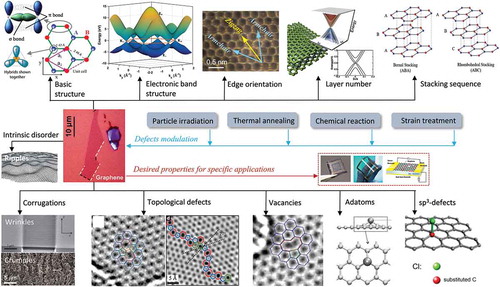
Monolayer graphene exhibits extraordinary properties owing to the unique, regular arrangement of atoms in it. However, graphene is usually modified for specific applications, which introduces disorder. This article presents details of graphene structure, including sp2 hybridization, critical parameters of the unit cell, formation of σ and π bonds, electronic band structure, edge orientations, and the number and stacking order of graphene layers. We also discuss topics related to the creation and configuration of disorders in graphene, such as corrugations, topological defects, vacancies, adatoms and sp3-defects. The effects of these disorders on the electrical, thermal, chemical and mechanical properties of graphene are analyzed subsequently. Finally, we review previous work on the modulation of structural defects in graphene for specific applications.
Graphical Abstract
1. Introduction
The first study on graphene, or two-dimensional graphite, can be dated to as early as 1947 when Wallace used the ‘tight binding’ approximation to investigate the electronic energy bands in crystalline graphite [Citation1]. Since it was shown that the semi-metallic phase is unstable in two dimensions [Citation2,Citation3], free standing monolayer graphene has long been regarded as an ‘academic’ material. Even so, many experimental efforts were made to obtain monolayer graphene. For instance, the monolayer graphene structures produced by hydrocarbon decomposition were observed on the Pt(111) surface under a scanning tunneling microscope (STM) in the early 1990s [Citation4]. In 1997, Japanese scientists cleaved a kish graphite for the purpose of evaluating the thickness effect of graphite crystals on electrical properties; they successfully reduced the thickness of graphite films to 30 nm [Citation5]. Inspired by this work, Novoselov and Geim presented a robust and reliable approach [Citation6] for producing monolayer graphene by repeatedly peeling highly oriented pyrolytic graphite (HOPG) in 2004. The demonstration of mechanical exfoliation method, also called the scotch tape method, caused a great sensation and stimulated many scholars to investigate the structure and properties of graphene.
As a single atomic plane of carbon, graphene can be wrapped up into other graphitic materials such as fullerene, carbon nanotubes and thin graphene films [Citation7]. Due to the internal exceptionally high crystal quality [Citation8,Citation9] and massless Dirac fermions [Citation10], monolayer graphene exhibits anomalous half integer quantum Hall effect [Citation11], remarkable optical properties [Citation12,Citation13], ultra-high intrinsic strength [Citation14], superior thermal conductivity [Citation15] and extremely high charge carrier mobility [Citation6,Citation16,Citation17]. It is referred to as a zero-gap semiconductor, showing an exceptionally high concentration of charge carriers and ballistic transport because of the unique Dirac cone band structure near the Fermi level. Moreover, the propagation of massless electrons through the honeycomb lattice in a sub-micrometer distance without scattering makes it possible to investigate the quantum effects in graphene even at room temperature [Citation18].
Graphene film consisting of few layers was employed to fabricate transistors, due to its strong ambipolar electric field effect [Citation6]. However, the performance of the graphene transistor was limited because of the low on-off resistance ratio (less than ~ 30 at room temperature) that resulted from the thermally excited carriers. Fortunately, the properties of graphene can be tuned by preparing graphene sheets using different approaches or by incorporating graphene sheets in different materials, rendering a path to a broad new class of graphene-based composites.
Graphene-based materials are expected to be promising building blocks in nanotechnology due to their varieties of applications, as seen in . For example, by optimization of the structure (i.e. interlayer spacing, thickness and morphology of graphene nanosheets) and by incorporation of carbon nanotubes or C60 molecules, the lithium storage capacity of graphene nanosheets could be increased up to above 700 mAh/g, making them suitable for use in rechargeable lithium ion batteries [Citation19]. The large surface area (2630 m2/g for a single graphene sheet) and high electrical conductivity (~ 200 S/m) gave a typical chemically modified graphene good performance in double layer capacitors [Citation20]. A large-area graphene film with high electrical quality was grown on a copper substrate by chemical vapor deposition (CVD), and it was successfully used to fabricate dual-gated field effect transistors, with Al2O3 as the gate dielectric [Citation21]. Quartz wafers, spin-coated by graphene oxide (GO) and annealed at a high-temperature (e.g. 1000 °C), exhibited a high-transparency, and showed great potential as heating, defrosting and antifogging devices [Citation22]. The batch production of large-area, uniform graphene films on solid glass was realized by a catalyst-free atmospheric-pressure CVD approach [Citation23]. Such graphene coated glass held good promise for thermochromic windows that benefit from the light interference effect of the changing layer thickness [Citation24]. Due to the excellent bendability and high electrical conductivity, graphene can be adopted as an appropriate transparent electrode material [Citation17,Citation25]. The unique optical and electrical properties allows graphene to be applied to various optoelectronic devices, ranging from solar cells to touch screens [Citation26]. Besides, graphene-based materials exhibit potential applications in catalysis [Citation27], owing to their high specific surface area and accessibility to the surface; in gas sensors [Citation28], owing to the sensitivity and selectivity of graphene towards various gas molecules; in waste energy harvesting [Citation29], because of their unique shape and characteristics such as superconductivity, light weight, high-stiffness and axial strength; in protective coatings [Citation30–Citation35] owing to the high intrinsic mechanical strength and anti-corrosion ability; and in antibacterial packing [Citation36]. More recent and comprehensive studies regarding applications of graphene can also be found in these reviews [Citation37–Citation42].
Figure 1. Applications of graphene and graphene-based materials in batteries, ultracapacitors [Citation20], water filters [Citation43], solar cells [Citation44], transistors and OLEDs [Citation26] (reused with permissions from [20] Copyright © 2008, American Chemical Society, [43] Copyright © 2012, American Chemical Society, and [44] Copyright © 2010, John Wiley and Sons.).
![Figure 1. Applications of graphene and graphene-based materials in batteries, ultracapacitors [Citation20], water filters [Citation43], solar cells [Citation44], transistors and OLEDs [Citation26] (reused with permissions from [20] Copyright © 2008, American Chemical Society, [43] Copyright © 2012, American Chemical Society, and [44] Copyright © 2010, John Wiley and Sons.).](/cms/asset/e71c34fd-9772-4a24-b68c-c7b30b108a98/tsta_a_1494493_f0001_oc.jpg)
The aforementioned applications are realized by the modification of graphene on the basis of defects modulation, during which specified types of disorders are quantitatively created for altering the crystal structure of graphene and consequently obtaining the wanted properties. Therefore, having a good understanding of the graphene structure and its contained disorders is necessary for defects modification. Although several review articles have already introduced the morphology and structure of graphene [Citation46,Citation47], and discussed the lattice defects in graphene [Citation48–Citation50], this review provides background knowledge of intrinsic structure of graphene before the introduction of disorders so that the function of disorders in graphene lattice can be more easily understood. Moreover, this review has added some content on recent studies regarding graphene. In this review, the basics of the graphene structure, electronic band structure of graphene, edge orientations in graphene, number and stacking sequences of graphene layers are initially introduced. Subsequently, the disorders that are commonly seen in the graphene structure, including corrugations, topological defects, vacancies, adatoms and sp3-defects, are discussed separately. Besides, the formation energy and migration energy of different types of structural defects are briefly introduced, and the effects of defects on properties of graphene and the generation of disorders during graphene preparation procedures are analyzed. Finally, previous studies on defects modulation of graphene by various approaches (e.g. particle irradiation, thermal annealing, chemical reaction and strain treatment) are reviewed.
2. The structure of graphene
2.1. Basics of graphene structure
Carbon is the sixth element in the periodic table, with a ground-state electronic configuration of , as shown in ). For convenience, the energy level of
is kept with no electron, though it is equivalent to the energy levels of
and
. As seen in ), the nucleus of a carbon atom is surrounded by six electrons, four of which are valence electrons. These electrons in the valence shell of a carbon can form three types of hybridization, namely sp, sp2 and sp3. ) illustrates the formation of sp2 hybrids. When carbon atoms share sp2 electrons with their three neighboring carbon atoms, they form a layer of honeycomb network of planar structure, which is also called monolayer graphene. The unit cell of a graphene crystal, marked by a purple parallelogram in ), contains two carbon atoms, and the unit-cell vectors a1 and a2 have the same lattice constant of 2.46 Å. The resonance and delocalization of the electrons are responsible for the stability of the planar ring.
Figure 2. (a) Atomic structure of a carbon atom. (b) Energy levels of outer electrons in carbon atoms. (c) The formation of sp2 hybrids. (d) The crystal lattice of graphene, where A and B are carbon atoms belonging to different sub-lattices, a1 and a2 are unit-cell vectors. (e) Sigma bond and pi bond formed by sp2 hybridization.
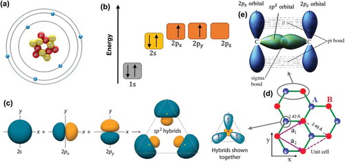
In a typical sp2 hybridization of two neighboring carbon atoms on the graphene layer (see )), an out-of-plane π bond is made up by orbitals which are perpendicular to the planar structure, while an in-plane σ bond is formed by the sp2 (
,
and
) hybridized orbitals. The resulting covalent σ bond has a short interatomic length of ~ 1.42 Å, making it even stronger than the sp3 hybridized carbon–carbon bonds in diamonds, thus giving the monolayer graphene remarkable mechanical properties (e.g. a Young’s modulus of 1 TPa and an intrinsic tensile strength of 130.5 GPa [Citation14]). In monolayer graphene, the conduction band and valence band with zero band gap are formed due to the half-filled π band that permits free-moving electrons. Further, the π-bonds provide a weak van der Waals interaction between adjacent graphene layers in bilayer and multi-layer graphenes.
Figure 3. (a) Honeycomb lattice of monolayer graphene, where white (black) circles indicate carbon atoms on A (B) sites, and (b) the reciprocal lattice of monolayer graphene, where the shaded hexagon is the corresponding Brillouin zone [Citation51] (reused with permission from [51] Copyright © 2011, Springer-Verlag Berlin Heidelberg.).
![Figure 3. (a) Honeycomb lattice of monolayer graphene, where white (black) circles indicate carbon atoms on A (B) sites, and (b) the reciprocal lattice of monolayer graphene, where the shaded hexagon is the corresponding Brillouin zone [Citation51] (reused with permission from [51] Copyright © 2011, Springer-Verlag Berlin Heidelberg.).](/cms/asset/5e6263b5-9828-4416-814b-7f6464b0685b/tsta_a_1494493_f0003_oc.jpg)
2.2. Electronic band structure of graphene
In the hexagonal lattice of monolayer graphene, as seen in ), two primitive lattice vectors are written as:
where Å is the lattice constant, which is the distance between unit cells. The position vector of atom
, (
= 1, 2, 3) relative to the atom
is denoted as
, and the three nearest-neighbor vectors in real space are given by
It is noted that is the spacing between two nearest-neighboring carbon atoms. ) illustrates the reciprocal lattice of monolayer graphene, where the crosses are reciprocal lattice points, and the shaded hexagon is the first Brillouin zone. The primitive reciprocal lattice vectors
and
satisfy the conditions,
therefore,
Normally, the electronic band structure of graphene can be calculated by using the LCAO method, which is also called tight-binding approach [Citation1,Citation52]. Hence, it is reasonable to start with the Bloch function
where is the wavefunction for the
orbitals localized at the position of
-atom, N is the number of lattice points, and G denotes a set of lattice vectors. By linearly combining the Bloch function for the two atoms in the unit cell of graphene lattice, we have the electronic eigenfunctions as
The transfer integral matrix, overlap integral matrix and column vector are given by
where the entries and
are given by
The diagonal transfer integral matrix elements can be derived from
As the dominant contribution comes from i = j, Equation 9 can be rewritten as
where is the energy of the
orbitals of carbon atoms.
Since carbon atoms on sub-lattice B are chemically identical to those on sub-lattice A, we have
Similarly, the diagonal overlap integrals can be calculated as
Assuming that the dominate contribution comes from the nearest three neighbors and other contributions are neglected, it is possible to write the off-diagonal transfer integral matrix element as
The value of the matrix element between each nearest-neighboring A and B atoms is the same, so
Then the off-diagonal transfer integral matrix elements can be written as
with
The function describing nearest-neighbor hopping can be evaluated as
in a similar fashion
with
Finally, the transfer and overlap integral matrices are obtained
The eigenvalues (j = 1, 2) can be written as
Substituting the expansion in terms of Bloch functions
Minimizing energy with respect to variations of
Written as a matrix equation:
The eigenenergies for graphene is then given by
By solving this secular equation, the expression for dispersion relation is derived as
where represent the conduction and valence bands respectively. The three parameters
,
and
can be found by comparison of tight-binding model with fitting experiments, or ab initio (from first principles) density functional theory (DFT) [Citation52]. Though it is Wallace who first employed tight-binding model to describe the band structure of graphene. The other nowadays better-known tight binding approximation was given by Saito et al. [Citation53] who considered the nonfinite overlap between the basic functions, but includes only interactions between nearest neighbors within the hexagonal lattice.
In a review by Saito et al. [Citation53], the values of ,
and
are suggested to be 0 eV, 3.033 eV and 0.129 eV. Here,
means that the energy of the 2
orbital is set to be equal to zero. The simulated band structure of graphene plotted in ) is consequently obtained by inputting these three values into the expression 28. Due to considerations of symmetry, the hopping of electrons between the two equivalent carbon triangular sub-lattices in the crystal structure of monolayer graphene leads to the formation of two energy bands (i.e. the upper conduction band and the lower valence band), which intersect at points where
is identically zero. Furthermore, the Fermi level is located at these points which are also named Dirac points.
Figure 4. (a) Band structure of graphene calculated with a tight-binding method with ,
and
. (b) Cross-section through the band structure, where the energy bands are plotted as a function of wave vector component
along the line
.
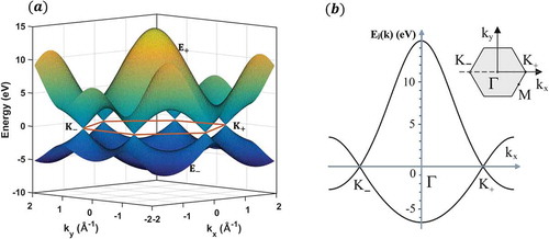
A particular line scan of the band structure is shown in ), where the energy bands are plotted as a function of wave vector component along the line
. In the inserted graph, the center of the Brillouin zone is labeled
, while two corners are labeled
and
separately. The dispersion near point
(
) is linear and can be described by a Dirac-like Hamiltonian [Citation54–Citation56]
where is the reduced Planck constant,
the Fermi velocity, and
the Pauli matrices. The asymmetry between the conduction band (
) and the valence band (
), which is especially pronounced in the vicinity of the
point, which is attributed to the non-zero overlap parameter
. However, the electronic band structure of graphene can be simply altered by applying electric field [Citation6,Citation57–Citation61] or providing substrates [Citation62,Citation63], and precisely engineered by introducing disorders into the hexagonal lattice [Citation64–Citation68], which will be discussed in detail in later sections.
2.3. Edge orientations in graphene
The chemical reactivity of monolayer graphene sheet at edges is at least twice that at basal planes, as suggested by spectroscopic tests and the electron transfer theory [Citation69]. It is also evidenced from STM analysis that edges of graphene can exhibit higher electronic density of states (DOS) near Fermi level than the basal planes [Citation70]. The edge configurations locally determine the distribution of electrons [Citation71], and thus the selection of crystallographic orientation of graphene is of crucial importance for controlling its electronic properties in localized states. Zigzag and armchair are two main types of edges along the crystallographic directions in graphene. In recent years, extensive studies were carried out to investigate the relative stability of these two edge orientations and the edge orientation-dependent physics for mechanically exfoliated monolayer graphene flakes [Citation72–Citation74], epitaxial graphene islands [Citation75–Citation77], CVD derived graphene grains [Citation78], and graphene nanoribbons (GNRs) [Citation79–Citation81].
In mechanical exfoliation of graphene flakes, the breaking is suggested to occur along the principle crystallographic directions [Citation7,Citation82]. Moreover, due to the hexagonal symmetry of graphene crystal (see )), the resulting edges of graphene flakes are expected to be terminated with either armchair or zigzag edges. As a consequence, the edges of mechanically exfoliated graphene flakes are mostly straight, and the angles between adjacent edges are often a multiple of 30° [Citation7,Citation72], as seen in ). On the other hand, zigzag directions appear to be more favorable for edges formed by certain etching reactions [Citation83,Citation84], or in holes created by electron beam irradiation in graphene [Citation85,Citation86]. The edge orientations in graphene flakes can be determined by using high-resolution STM which is capable of providing atomic resolution images of the graphene crystal lattice for unambiguous identification of armchair or zigzag edges [Citation72]. Edge orientations of monolayer graphene can also be identified by G mode in Raman spectroscopy [Citation73], as G modes at zigzag- or armchair-dominated edges of monolayer graphene exhibit different polar behaviors. Xu et al [Citation74] employed polarized Raman spectroscopy to investigate the thermal stability and dynamics of graphene edges, and they found that both zigzag and armchair edges were unstable and underwent modifications even at 200 °C. Hyun et al. [Citation87] further suggested that the edges of graphene flake have predominantly zigzag terminations below 400 °C, while the edges would be dominated by armchair and reconstructed zigzag edges above an annealing temperature of above 600 °C. Recent studies on the processes and mechanisms which drive the chemical functionalization of graphene edges are reviewed by Bellunato et al. [Citation71].
Figure 5. (a) Scanning electron microscopy (SEM) image of a relatively large graphene crystal, which shows that most of the crystal’s faces are zigzag and armchair edges, as indicated by blue and red lines and illustrated in the inset [Citation7]. (b) A typical graphene flake obtained by micromechanical cleavage [72]. (c) Sketch of the honeycomb crystal lattice of graphene. Two distinct crystallographic orientations of a graphene crystal, rotated against each other in multiples of 30°, are indicated as armchair type (solid lines) and zigzag type (dashed lines) [Citation72]. (d) CC-STM image of edges of graphene on Ir(111), with crystallographic directions of the Ir substrate denoted at the top-right side [Citation89]. (e) STM image of graphene structures on Co substrate, and schematic of triangular and hexagonal corners, respectively, for zigzag-edged graphene structures on Co(0001) [Citation90]. (f) 20 × 20 nm2 STM image and (g) 2.5 × 2.5 nm2 rendered STM topography of graphene island on 6H-SiC(0001) substrate. Overlaid on this image are the two lowest energy edge directions: zigzag (yellow arrow) and armchair (blue arrows) [Citation75] (reused with permissions from [7] Copyright © 2007, Springer Nature, [72] Rights managed by AIP Publishing, [89] Copyright © 2012 American Physical Society, [90] Copyright © 2014, American Chemical Society, and [75] Copyright ©2010 American Physical Society.).
![Figure 5. (a) Scanning electron microscopy (SEM) image of a relatively large graphene crystal, which shows that most of the crystal’s faces are zigzag and armchair edges, as indicated by blue and red lines and illustrated in the inset [Citation7]. (b) A typical graphene flake obtained by micromechanical cleavage [72]. (c) Sketch of the honeycomb crystal lattice of graphene. Two distinct crystallographic orientations of a graphene crystal, rotated against each other in multiples of 30°, are indicated as armchair type (solid lines) and zigzag type (dashed lines) [Citation72]. (d) CC-STM image of edges of graphene on Ir(111), with crystallographic directions of the Ir substrate denoted at the top-right side [Citation89]. (e) STM image of graphene structures on Co substrate, and schematic of triangular and hexagonal corners, respectively, for zigzag-edged graphene structures on Co(0001) [Citation90]. (f) 20 × 20 nm2 STM image and (g) 2.5 × 2.5 nm2 rendered STM topography of graphene island on 6H-SiC(0001) substrate. Overlaid on this image are the two lowest energy edge directions: zigzag (yellow arrow) and armchair (blue arrows) [Citation75] (reused with permissions from [7] Copyright © 2007, Springer Nature, [72] Rights managed by AIP Publishing, [89] Copyright © 2012 American Physical Society, [90] Copyright © 2014, American Chemical Society, and [75] Copyright ©2010 American Physical Society.).](/cms/asset/d917062c-d5b1-4f88-ae49-a3d137f3aed9/tsta_a_1494493_f0005_oc.jpg)
Graphene islands are of great scientific interest due to their small sizes which are suspected to yield novel electronic properties (e.g. quantum confinement [Citation88]). The edge orientations of epitaxial graphene islands are found to be strongly influenced by the underlying substrates. For example, graphenenano-islands that are epitaxially grown on monocrystalline metal surfaces (i.e. Ir(111) [Citation76,Citation89], Co(0001) [Citation77,Citation90] and Pt(111) [Citation91]) have mostly zigzag terminations, whereas those grown on 6H-SiC(0001) are dominated by armchair edges [Citation75]. The constant-current STM (CC-STM) image of edges of graphene on Ir(111) can be seen in ), where the gray mesh indicates the moire superstructure on graphene, and the blue and yellow arrows represent the zigzag graphene edges on substrate surface and at substrate step edges respectively. It is evidenced from low-temperature transmission electron microscopy (TEM) measurements that graphene structures exhibit an on-top registry with respect to the Co(0001) surface [Citation77]. A detailed analysis of the on-top registry reveals that the straight edges of graphene on clean Co surface are mainly terminated in zigzag directions. With fixed edge chirality, commensurate graphene can form islands on Co(0001) substrate with either triangular or hexagonal corners, as seen in ) [Citation90]. In the first case, the peripheral atoms maintain the same registry, whereas, in the second case, adjacent edges exhibit opposite configurations. From ), the edges of the graphene island which are highlighted by overlaying two blue arrows are in alignment with the lattice vector directions of underlying SiC substrate (see the red arrows in the inset) [Citation75]. An atomic-resolution STM image of the step edges of this graphene island is provided in ), where the blue and yellow arrows indicate armchair and zigzag directions respectively. By comparing the arrows in , the graphene island is ascertained to be entirely surrounded by armchair edges.
In the CVD growth of polycrystalline graphene, graphene boundaries (GBs) are formed by coalescence of the graphene grains that initially nucleate from random and uncontrollable locations. These GBs can impede electron transport [Citation92] and degrade the mechanical properties of the resulting films [Citation93]. ) indicates the formation of isolated grains and merged grains at the early stage of ambient CVD growth of graphene on Cu substrates [Citation78]. As shown in ), Raman mapping of the D peak intensity can provide a clear identification of the locations of grain boundaries between two coalesced grains, which cannot be visualized by simply using SEM or atomic force microscopy (AFM). The few isolated spots displaying relatively large D peak intensities are suggested to be the nucleation centers where the CVD-growth of graphene is initiated [Citation78]. Pronounced D peak intensities were also observed at the grain edges, consistent with previous Raman studies [Citation94,Citation95]. The edge orientations of graphene grains can be determined by comparing their TEM images in real space with the corresponding selected area electron diffraction (SAED) patterns (see the supplementary information in Ref [Citation78].). By using this identification method, most of the grain edges were found to be approximately aligned with zigzag directions. The bright filed TEM image of a typical hexagonally shaped graphene grain and its characteristic SAED pattern (inset) are given in ), where the dashed lines correspond to the zigzag directions. ) shows a large-scan-area STM topography image of a graphene grain near a hexagonal corner, and the atomic-resolution STM image in ) is taken from the area marked by a black square in ). By comparing the grain edges (white dashed lines) in ) with the crystal directions (zigzag versus armchair) in ), it is confirmed that the edges of CVD derived hexagonal grains are mostly bounded by zigzag terminations.
Figure 6. (a) SEM image of an annealed Cu foil taken out of the furnace after graphene growth [Citation78]. (b) Intensity map of D band for two coalesced graphene grains [Citation78]. (c) A montage of bright field TEM images (80 kV) spliced together to show an example of a hexagonally shaped graphene grain, with its characteristic SAED pattern in the inset [Citation78]. (d) STM topography image taken near a corner of a graphene grain on Cu [Citation78]. (e) Atomic-resolution STM image taken from the area which is marked by a black square in Figure 6(d). (Z: zigzag; A: armchair) [Citation78]. (f) A modified HRTEM image of overlapping zigzag-armchair edges; the HRTEM image is originally from Ref [Citation79], and the modified version is from Ref [Citation111] (reused with permissions from [78] Copyright © 2011, Springer Nature, [79] Copyright © 2009, American Association for the Advancement of Science, and [111] Copyright © 2010 Elsevier Ltd.).
![Figure 6. (a) SEM image of an annealed Cu foil taken out of the furnace after graphene growth [Citation78]. (b) Intensity map of D band for two coalesced graphene grains [Citation78]. (c) A montage of bright field TEM images (80 kV) spliced together to show an example of a hexagonally shaped graphene grain, with its characteristic SAED pattern in the inset [Citation78]. (d) STM topography image taken near a corner of a graphene grain on Cu [Citation78]. (e) Atomic-resolution STM image taken from the area which is marked by a black square in Figure 6(d). (Z: zigzag; A: armchair) [Citation78]. (f) A modified HRTEM image of overlapping zigzag-armchair edges; the HRTEM image is originally from Ref [Citation79], and the modified version is from Ref [Citation111] (reused with permissions from [78] Copyright © 2011, Springer Nature, [79] Copyright © 2009, American Association for the Advancement of Science, and [111] Copyright © 2010 Elsevier Ltd.).](/cms/asset/06135e27-bfa4-4bb0-b3a1-38246eee0d1e/tsta_a_1494493_f0006_oc.jpg)
With decreasing size, the surface free energy of a material increases, and its properties start depending on the surface interactions. This size effect is more significant for nanomaterials, with an average size of 1–100 nm, for most of their atoms are exposed to the surface and interact with the surroundings. For the same reason, the electronic structure of GNRs that have ultrathin width of less than 10 nm are quite sensitive to their edge orientations. The approaches for synthesis of GNRs include epitaxial growth on templated silicon carbide (SiC) substrates [Citation96], CVD growth on structured substrates (e.g. steps [Citation97], twins [Citation98], and trenches [Citation99]), and directly partial growth on germanium(001) [Citation100]. The lattice of GNR shows both zigzag and armchair edge orientations which can be observed by using AFM [Citation101] and STM [Citation79,Citation100]. ) illustrates a modified high-resolution TEM (HRTEM) image of overlapping zigzag-armchair edges. Normally, GNRs with a higher fraction of zigzag edges exhibit a smaller energy gap than a predominantly armchair-edge ribbon of similar width [Citation80]. On the basis of tight binding theory, the zigzag GNRs are always metallic, while the armchair GNRs exhibit either metallic or semiconducting behaviors, depending on their width. For instance, DFT shows that the energy band gaps of semiconducting armchair GNRs increase as their width decreases [Citation81]. This property of armchair GNRs is also evidenced from experiments [Citation102]. Therefore, the electronic structure of GNRs can be engineered by modification of local structure of edge [Citation103], altering GNR configuration (e.g. width and crystallographic orientation) [Citation104,Citation105] as well as electron–electron and spin–orbit interactions [Citation59,Citation106]. More detailed information about the design of electronic properties of GNRs was given by Dutta and Pati [Citation107] and Yazyev et al. [Citation108].
2.4. Number of graphene layers
The term graphene theoretically refers to monolayer graphene [Citation109], and sometimes also includes bilayer graphene, as both of them are semimetals with no overlap between the valence and conduction bands [Citation7]. The electronic structure of few-layer graphene (FLG, number of layers from 3 to < 10), is more complex because of the appearance of charge carriers. It has been shown that the electronic structure of graphene rapidly evolves with the number of layers, approaching the 3D limit of graphite at 10 layers [Citation110].
illustrates the low-energy DFT 3D band structure and its projection on component close to K point for monolayer, bilayer, and trilayer graphenes and bulk graphite [Citation111]. In the energy spectrum of monolayer graphene, the conduction band and valence band touch at Dirac points, and the electron dispersion near these points is linear. In monolayer graphene, there is no underneath carbon atom for the
orbital to interact with, whereas this possibility exists in bilayer graphene, which enables the formation of a zero-energy band. Owing to the presence of massive chiral quasiparticles with parabolic dispersion at low energy [Citation112], the integer quantum Hall effect in bilayer graphene [Citation113] can be even more unusual than that in monolayer graphene. ) shows the four parabolic bands, as the (AB-stacked) bilayer graphene has four atoms in the unit cell. The band structure of bilayer graphene can be tuned by applying an electric field [Citation114,Citation115], providing appropriate substrates [Citation116] or chemical modulations [Citation117,Citation118], which is expected to attract interests in nanoelectronic and nanophotonic applications [Citation119]. From ), the band structure of (ABA-stacked) trilayer graphene seems to be a combination of those of monolayer and (AB-stacked) bilayer. However, trilayer graphene is actually a semimetal with a conductivity that increases with increasing electric field. This behavior significantly differs from that of monolayer and bilayer graphene, which is originated from the presence of a finite overlap between valence and conduction band [Citation120]. Moreover, as effective mass of graphene increases with the increasing layer thickness, trilayer graphene exhibits lower mobility than those of monolayer and bilayer [Citation121]. In general, the low-energy spectrum of FLG with odd number of layers is a combination of one massless Dirac mode and
massive Dirac modes per spin and valley, whereas all N modes are massive at low-energies for even number of layers. Therefore, for FLG with N layers (AB stacking), there will be
electronlike and
holelike parabolic bands and an additional linear energy band (Dirac fermions) around K point [Citation122] if N is odd; Otherwise, there will be only
electronlike and
holelike parabolic bands around K point. Because of a significant overlap between the conduction and valence bands, FLG thicker than five layers shows a semi-metallic band structure with parabolic-like bands, which is highly similar to that of bulk graphite, as seen in ).
Figure 7. Low energy DFT 3D band structure and its projection on component close to K point for (a) monolayer graphene, (b) AB-stacked bilayer graphene, (c) ABA-stacked trilayer graphene and (d) bulk graphite. The Fermi level has been set at zero in all cases [Citation111] (reused with permission from [111] Copyright © 2010 Elsevier Ltd.).
![Figure 7. Low energy DFT 3D band structure and its projection on kx component close to K point for (a) monolayer graphene, (b) AB-stacked bilayer graphene, (c) ABA-stacked trilayer graphene and (d) bulk graphite. The Fermi level has been set at zero in all cases [Citation111] (reused with permission from [111] Copyright © 2010 Elsevier Ltd.).](/cms/asset/7a9e1118-294f-41fa-8a56-dcd02d7879c4/tsta_a_1494493_f0007_oc.jpg)
Not surprisingly, properties of bilayer graphene are quite similar to those of monolayer graphene. These properties include excellent room temperature electrical conductivity with mobility of up to 40,000 cm2 V−1 s−1 [Citation123], high room temperature thermal conductivity of about 2800 W m−1 K−1 [Citation124,Citation125], outstanding mechanical stiffness and strength with a Young’s modulus of about 0.8 TPa [Citation126,Citation127], fine transparency with white light transmittance of about 95% [Citation128], and impermeability to gases [Citation129]. Zhang and Gu [Citation130] carried out molecular dynamics (MD) simulations on multi-layer graphene with layer number varying from one to seven, and found that the mechanical properties (i.e. Young’s modulus, fracture stress and fracture strain) of graphene were sensitive to the temperature changes rather than the layer numbers and isotope substitutions. Lee et al. [Citation131] conducted tensile and friction testing of graphene sheet (with 1–4 layers) by using AFM tips. The experimental results indicated that little difference was found in the intrinsic stiffness and strength of sample with 1–3 atomic layers, while the friction force between AFM tip and graphene sheet decreases as the layer number increases from 1 to 4. In the calculation model established by Xiao et al. [Citation132], the electrical conductivity of few-layer graphene with layer number of 2–9 reduced as the thickness increased, and the reduction of conductivity was mainly caused by the inhibited carrier mobility. Further, the conductivity decreased rapidly with increasing thickness when the number of graphene layers ranged from 2 to 13, but decreased slowly and thereafter remained constant for layer numbers up to 165. These numerical simulation results were in agreement of the published experimental results [Citation133,Citation134]. More information about the properties of monolayer, bilayer and few-layer graphene can be found in Refs [Citation119,Citation135–Citation139].
The 514 nm and 633 nm Raman spectra around the wavenumber of 2700 for graphenes with various numbers of layers are compared in . By examination of the location and shape of defect-activated D peak and the most two prominent features (G and G’ peaks) in the Raman spectra of graphenes with less than five layers, the number of graphene layers can be effectively identified without ambiguity [Citation140,Citation141]. However, the Raman spectrum of FLG thicker than five layers can be hardly distinguished from that of bulk graphite, as the stepwise broadened 2D band approaching that of bulk graphite due to continuous splitting of valence and conduction bands. The number of graphene layers can also be determined by SEM [Citation142], Auger electron spectroscopy (AES) [Citation143], nanoindentation [Citation144], optical reflection microscopy [Citation145] and surface plasmon resonance (SPR) [Citation146,Citation147].
Figure 8. Evolution of the (a) 514 nm and (b) 633 nm Raman spectra near the 2D peak with the number of graphene layers [Citation140] (reused with permission from [140] Copyright © 2006 American Physical Society.).
![Figure 8. Evolution of the (a) 514 nm and (b) 633 nm Raman spectra near the 2D peak with the number of graphene layers [Citation140] (reused with permission from [140] Copyright © 2006 American Physical Society.).](/cms/asset/4a757497-6b61-4df7-8e52-749b5ec5037b/tsta_a_1494493_f0008_b.gif)
Recently, multiple attempts have been made to precisely control the number of layers for the purpose of tuning the electronic band structure of graphene [Citation111]. For e.g. Lin et al. [Citation148] used a picosecond laser to remove graphene layers from multi-layered graphene films. As both the lateral size and the crystallinity of the starting graphite influenced the number of graphene layers obtained by chemical exfoliation, Wu et al. [Citation149] successfully tuned the number of graphene layers by selecting appropriate starting materials from artificial graphite, flake graphite powder, Kish graphite, and natural flake graphite. In that study, the number of graphene layers was measured by AFM.
2.5. Stacking arrangements of graphene layers
The crystallographic stacking of graphene sheets provides additional degrees of freedom, thus leading to countless stacking sequences [Citation150,Citation151]. The different stacking orders of the honeycomb network of planar structures strongly influence the interlayer screening [Citation152], band structure [Citation153,Citation154], and spin–orbit coupling [Citation155] of the resulting graphene films. The stacking arrangements of bilayer graphenes can be either AA or AB, which are shown in . For AA stacking, each carbon atoms in the second layer directly aligned on the top of another atom in the first layer, while in bilayer graphene with Bernal or AB stacking, a set of atoms in the second layer sit over the empty centers of hexagons in the first layer. As seen in the scanning transmission electron microscopy (STEM) image of AA-stacked bilayer graphene (see )) [Citation156], all atomic sites are visible in a hexagonal array and show similar brightness. Whereas in Bernal-stacked bilayer, bright spots having hexagonal symmetry and a spacing of 0.25 nm (close to ) are observed in ). These spots, which correspond to the sites where two atoms are stacked on top of one another, are threefold to fourfold brighter than that of individual atoms because of the coherent scattering.
Figure 9. Stacking arrangements and hopping parameters for (a) AA-stacked and (b) AB-stacked bilayer graphene [Citation166]. Hopping integrals t and t’ correspond to the in-plane nearest-neighboring and next-nearest-neighboring hopping respectively, and parameter is associated with the main interlayer hopping in bilayer. Atomic-resolution STEM images of (c) AA- and (d) AB-stacked bilayer graphenes [Citation156]. Hexagonal ring in the first (second) or bottom (top) layer is marked with green (orange) color. (e) Low energy dispersion and (f) low energy DOS for a bilayer graphene with AA stacking. (g) Low-energy dispersion and (h) low-energy DOS for a bilayer graphene with AB stacking [Citation157] (reused with permissions from [166] © 2016 Elsevier B.V., and [157] Copyright © 2012 American Physical Society.).
![Figure 9. Stacking arrangements and hopping parameters for (a) AA-stacked and (b) AB-stacked bilayer graphene [Citation166]. Hopping integrals t and t’ correspond to the in-plane nearest-neighboring and next-nearest-neighboring hopping respectively, and parameter t0 is associated with the main interlayer hopping in bilayer. Atomic-resolution STEM images of (c) AA- and (d) AB-stacked bilayer graphenes [Citation156]. Hexagonal ring in the first (second) or bottom (top) layer is marked with green (orange) color. (e) Low energy dispersion and (f) low energy DOS for a bilayer graphene with AA stacking. (g) Low-energy dispersion and (h) low-energy DOS for a bilayer graphene with AB stacking [Citation157] (reused with permissions from [166] © 2016 Elsevier B.V., and [157] Copyright © 2012 American Physical Society.).](/cms/asset/28a9596c-65c8-4779-a573-e02190798238/tsta_a_1494493_f0009_oc.jpg)
Bilayer graphene has not only in-plane hopping (e.g. nearest neighboring hopping and next nearest neighboring) in the same layer, just like that in monolayer graphene, but also vertical hopping which is dependent on the stacking order. In the case of AA-stacked bilayer graphene, vertical hopping mainly occurs between –
sites and
–
sites, while in AB-stacked bilayer, the vertical hopping can be very complex: besides the hopping between the dimer sites
, it is possible to introduce the hopping
from a non-dimer site to nearest non-dimer sites in the opposite layer, and hopping
from a dimer site to nearest non-dimer sites of the opposite layer. Consequently, subtle difference exists in the electronic structure of bilayer graphene with different stacking orders.
The single spin Hamiltonians for AA-stacked and AB-stacked bilayer graphene and their corresponding matrix representations are given in Refs [Citation157,Citation158]. By calculation of the eigenvalues of these two matrices, the band structures of two types of bilayer are obtained and the corresponding low-energy parts are plotted in . Analytic expressions for the total double spin DOS of two bilayers are derived from the sum of two Dirac cone DOS which are shifted relative to each other by , and two plots of low-energy DOS are then compared in ,h). Because of the differences in electronic structure, AA-stacked and AB-stacked bilayers exhibit different optical conductivity [Citation157] and responses to an external electric field [Citation159]. The energy gap of bilayer graphene can be artificially opened by application of a perpendicular electric field [Citation160], hence a controlled induction of an insulating state in bilayer graphene can be realized by using a dual-gate device [Citation161]. Although AB stacking is energetically the most favorable in bilayer graphene, the non-AB stacking (e.g. AA stacking and AA’ stacking) regions can be stabilized by means of creating stacking boundaries [Citation162] or introducing a minute twist [Citation163]. Moreover, the formation of closed edges between adjacent graphene layers results in that AA stacking is more frequently seen in bilayer graphene so that the local strains can be reduced [Citation164]. Further, extensive theoretical and experimental studies have been carried out to explore the properties of AA-stacked [Citation157,Citation164–Citation166] and Bernal-stacked [Citation139,Citation158,Citation167,Citation168] bilayer graphenes.
The stacking orders can become more complicated for multi-layer graphene. Theoretically, there are two stable stacking arrangements, namely Bernal (in ABA stacking order) and rhombohedral (in ABC stacking sequence), as seen in ), and Bernal structures are presumed to be slightly more thermodynamically stable. In both cases, the stacking of graphene layers is attributed to the weak interaction between π bonds in the adjacent basal planes, and these two structural configurations have the same stacking distance of 0.3354 nm between sheets. However, the stacking sequence of FLG is experimentally found to exert pronounced influence on the electronic band structure [Citation150], which are compared in ,d), and thus the electrical properties of FLG with different stacking sequences are expected to be distinct to some extent. For example, the Bernal trilayer is viewed as a semimetal with electrically tunable band overlap [Citation120,Citation169–Citation171], while the rhombohedral trilayer is predicted to be a semiconductor with a band gap that can be electrically tuned [Citation153,Citation169,Citation170]. Moreover, the application of a certain electric field can finally open larger band gap in the latter than that in the former [Citation153,Citation172].
Figure 10. (a) Bernal and (b) rhombohedral stacking arrangements in multilayer graphene. Electronic band structures of (c) Bernal-stacked and (d) rhombohedral stacked tetralayer graphenes [Citation150]. (e)Raman imaging of the distribution of ABA and ABC trilayer graphene domains [Citation174]. (f) Raman 2D-mode spectra for the tetralayer graphene samples of ABAB (green line) and ABCA (red line) stacking orders [Citation174](reused with permissions from [150] Copyright © 2010 American Physical Society, and [174] Copyright © 2011, American Chemical Society.).
![Figure 10. (a) Bernal and (b) rhombohedral stacking arrangements in multilayer graphene. Electronic band structures of (c) Bernal-stacked and (d) rhombohedral stacked tetralayer graphenes [Citation150]. (e)Raman imaging of the distribution of ABA and ABC trilayer graphene domains [Citation174]. (f) Raman 2D-mode spectra for the tetralayer graphene samples of ABAB (green line) and ABCA (red line) stacking orders [Citation174](reused with permissions from [150] Copyright © 2010 American Physical Society, and [174] Copyright © 2011, American Chemical Society.).](/cms/asset/df089ca3-08bb-4331-9afc-fea397955691/tsta_a_1494493_f0010_oc.jpg)
The controlled growth of FLG with specified stacking sequences can be performed in the chamber of an environmental scanning electron microscope (ESEM) which enables real-time imaging of the shape and size evolution of graphene islands [Citation173]. Infrared (IR) absorption/reflection spectroscopy can be used to characterize the stacking order in graphene [Citation124], but this technique has a low spatial resolution [Citation150]. In contrast, the stacking structures in tri- and tetralayer graphenes are readily visualized by Raman imaging, owing to the clear associations with the distinctive line shapes and widths in the Raman 2D mode [Citation174] (see )). The stacking order and corresponding number of layers in multi-layer graphene can also be characterized by TEM [Citation175].
3. Disorders in graphene structure
An ideal graphene with highly ordered structures exhibits zero band gap [Citation6], high tensile strength [Citation14] and high thermal conductivity [Citation15] at room temperature. Despite such outstanding properties, the potential applications of atom-thick graphene are limited, so it needs to be incorporated with other materials or assembled into nanopapers [Citation176–Citation178], functional thin films [Citation179], fibers [Citation180,Citation181] and coatings [Citation30,Citation182] for meeting various demands in industry. Some properties of graphene might be enhanced when completing the assembling processes, but large disorder is introduced to the graphene crystal as well. Disorders can also be brought into the crystal structure of graphene during the synthesis process. These disorders can be generally categorized as corrugations, topological defects, adatoms, vacancies and sp3-defects. Therefore, this part will first introduce the configurations of diverse types of disorders contained in the crystal structure of graphene in detail, followed by a brief discussion about the formation energy and immigration energy of these disorders. After that, the influence of different types of disorders on properties of graphene are analyzed. Lastly, we will introduce the generation of various disorders during graphene preparation procedures, and provide approaches for reducing these disorders, so that near-defect-free samples of monolayer graphene can be obtained.
3.1. Corrugations
In the standard harmonic approximation [Citation183], the long-range order of two-dimensional lattices should be destroyed by thermal fluctuation, so a perfectly flat graphene is presumed to be non-existent [Citation3,Citation184]. Moreover, it is experimentally proven [Citation185–Citation187] that ultrathin films with only dozens of layers are thermodynamically unstable unless they inherently constitute a part of three-dimensional structures (e.g. a substrate with a matching lattice). Indeed, the atomically thin film can be significantly stabilized by partially decoupled bending and stretching modes [Citation188]. By using TEM, a monolayer graphene was found to be freely suspended on a microfabricated metallic scaffold in both vacuum and air at room temperature, with random elastic deformations in the third dimension [Citation9]. The asymmetric distribution of carbon–carbon bond lengths resulting from the localized π electrons forces the graphene lattice to become non-planar for minimizing free energy, thus leading to the formation of ripples with heights up to 1 nm. Therefore, the thermal fluctuations induced ripples are intrinsic features on graphene sheets. As observed under STM [Citation189], these spontaneous ripples on the suspended graphene are dynamic. Plus, the density of the ripples is higher near the edges or defects due to the amplified asymmetry of the bond lengths at these regions [Citation188,Citation190]. The amplitude of ripples is limited by the strain energy induced by its perpendicular displacement, and increases with the size of graphene sheet [Citation191]. The spatial distributions of ripples can be derived from the equation [Citation188]:
where L is the distance between two ripples, the bending rigidity, T the absolute temperature and B the two-dimensional bulk modulus. The equation indicates that the distance between two ripples is inversely proportional to the square root of the temperature, and approaches infinity at the temperature of 0 K.
Figure 11. A summary illustration of three types of corrugations (i.e. ripples, wrinkles and crumples) [Citation192]. (reused with permission from [192] © 2015 The Authors. Published by Elsevier Ltd.).
![Figure 11. A summary illustration of three types of corrugations (i.e. ripples, wrinkles and crumples) [Citation192]. (reused with permission from [192] © 2015 The Authors. Published by Elsevier Ltd.).](/cms/asset/55289588-7098-4c66-b762-87f9bd34723b/tsta_a_1494493_f0011_oc.jpg)
Apart from the intrinsic disorder of ripples, wrinkles and crumples are other two types of corrugations in graphene sheets [Citation192] (see ). Unlike ripples having a modest aspect ratio of ~ 1 and feature sizes of peaks and valleys below 10 nm, wrinkles exhibit a high aspect ratio of 10, and the width ranges from 1 to 10 nm, the height below 15 nm and the length above 100 nm [Citation193]. Wrinkles normally occur on metallic substrates due to the opposite thermal deformation [Citation194,Citation195] and the defect lines [Citation196] on the substrates. Also, the thickness of growth substrate has an effect on the attributes and density of wrinkles. For instance, as the thickness of nickel substrate increases, the grain size of supported graphene decreases, leading to higher-density and smaller wrinkles on graphene sheet [Citation194]. Wrinkles can also be generated by water drainage between graphene and substrate in the graphene transfer processes. The relation between wavelength () and amplitude (
) of wrinkles on suspended FLG resulted from longitudinal stretching strain [Citation197] can be described by [Citation198]
where and L are the thickness and width of a graphene thin film respectively, and
is the Poisson’s ratio which is predicted to be 0.1–0.3 for monolayer graphene [Citation199,Citation200]. However, the relation needs to be revised slightly when in-plane shear dominates the applied stress [Citation198]:
As the values of ,
,
and
can be measured from AFM images, plotting
versus
allows the determination of the type of applied stress [Citation198]. When using the buckling theory to calculate the wrinkling wavelength of the pre-strained substrate-supported graphene thin film, the substrate is assumed to exhibit stress–strain behavior complying with Hooke’s law but be non-linear at large deformations, so we have:
where is the thickness of the graphene film,
the Young’s modulus of graphene,
the shear modulus of substrate,
the Poisson’s ratio and
, for
, where
and
are pre-strain and initial length of the substrate respectively [Citation201].
Crumples are dense deformations that are generated by rapid evaporation, usually occurring isotropically in two or three dimensions [Citation189,Citation201]. For example, submicrometer-size ball-like crumpled graphene structures can be produced by isotropic compression and thermal reduction of GO [Citation202]. Ma et al. [Citation203] also reported the fabrication of few hundred nanometer-size crumped graphene ball by rapid drying of GO. Unlike wrinkled graphene that experiences deformation by uniaxial confining forces, crumpled graphene undergoes multidirectional compression. The increasing lateral compression force makes the graphene thin film to transform from flat to cone and finally to crumple ball [Citation204]. When the compression force is larger than the crumpling threshold state (), the radius of graphene sheet decreases to 63% of its initial value, and is nearly independent of force. In this case, the crumpled graphene sheet is expected to follow a power-law behavior, and has a scaling form [Citation204] as:
where and
are sheet radius under force and the initial sheet radius respectively,
the 2D Young’s modulus,
the bending rigidity, F the compression force, and C,
,
the scaling parameters.
3.2. Topological defects
The graphenes produced via the CVD method are usually polycrystalline, due to the presence of topological defects: disclinations, dislocations and GBs, which are able to alter the lattice orientations. An intriguing feature of these topological defects is that they can exist in graphene without introducing local disorder into crystalline lattice. ) shows the configuration of disclinations which are elementary topological defects in the graphene sheet, resulting from the addition or removal of semi-infinite wedges. For example, the positive wedge angle (s = 60°) allows a pentagon to be embedded into the honeycomb lattice of graphene, while the negative wedge angle (s = −60°) creates a heptagon embedded in the graphene lattice. The isolated non-hexagonal rings in graphene inevitably result in non-planar structures.
Figure 12. Configurations of (a) disclinations and (b) dislocations in graphene lattice [Citation207] (reused with permission from [207] Copyright ©2010 American Physical Society.).
![Figure 12. Configurations of (a) disclinations and (b) dislocations in graphene lattice [Citation207] (reused with permission from [207] Copyright ©2010 American Physical Society.).](/cms/asset/08b94831-b813-4cd5-adcb-22291da7436c/tsta_a_1494493_f0012_oc.jpg)
As seen in ), dislocations are topological defects that are equivalent to the pairs of complementary disclinations. The topological invariant of a dislocation is the Burgers vector , which is a proper translational vector of graphene lattice:
where and
are lattice vectors, and the pair of integers (m, n) is used as a description of the dislocation. The Burgers vector is related to the distance between two disclinations on graphene lattice. Dislocation (1,0) shows the smallest Burgers vector (
Å) that is achieved by an edge-sharing heptagon-pentagon dislocation which inserts a semi-infinite strip of atoms along the armchair high-symmetry direction in graphene. Whereas the (1,1) dislocation has a longer Burgers vector (
Å), and the semi-infinite strip is inserted along the zigzag direction. The core of dislocation with a Burgers vector the same as that of dislocation (1,1) can be also constructed from two dislocations, such as (1,0)+(1,1) dislocation pair.
GBs can be viewed as a type of line defects formed by one-dimensional chains of aligned dislocations [Citation205], which form the interface between the domains of material with different crystallographic orientations. The misorientation angle θ = θL + θR (0° < θ < 60°), describing the mutual orientation of the two crystalline domains, is a critical topological invariant of GBs. illustrate the configurations of the and the
symmetric large-angle GBs, respectively. Small-angle GBs with misorientation angles close to 0° or 60° are thought to be along armchair or zigzag directions respectively. According to Frank’s equation [Citation206], the misorientation angle resulted from aligning (1,0) dislocations along the grain-boundary line is related to the separation between the neighboring dislocations
and their Burgers vectors
:
Higher densities of dislocations correspond to smaller separations between neighboring dislocations, and consequently are expected to lead to larger misorientation angles. Further, the small-angle GBs in suspended graphene tend to form the out-of-plane buckling for further reducing their formation energies, while large-angle GBs are almost flat [Citation207].
Figure 13. Configurations of (a) the θ = 21.8° and (b) the θ = 32.2° symmetric large-angle GBs, respectively [Citation137]. (c) STM image of a regular line defect in graphene on the Ni(111) [Citation208]. (d) Aberration-corrected annular ADF-STEM image of two grains which intersect with a relative rotation of 27°, and are stitched together by an aperiodic line of dislocations [Citation209]. (e) Electron diffraction pattern obtained by DF-TEM imaging graphene grains one by one with few-nanometer resolution using an objective aperture filter in the back focal plane through a small range of angles, and repeating this process using several different aperture filters. (f) False-color, DF image overlay of the sizes, shapes and orientations of several grains [Citation209] (reused with permissions from [137] Copyright © 2014, Springer Nature, [208] Copyright © 2010, Springer Nature, and [209] Copyright © 2011, Springer Nature.).
![Figure 13. Configurations of (a) the θ = 21.8° and (b) the θ = 32.2° symmetric large-angle GBs, respectively [Citation137]. (c) STM image of a regular line defect in graphene on the Ni(111) [Citation208]. (d) Aberration-corrected annular ADF-STEM image of two grains which intersect with a relative rotation of 27°, and are stitched together by an aperiodic line of dislocations [Citation209]. (e) Electron diffraction pattern obtained by DF-TEM imaging graphene grains one by one with few-nanometer resolution using an objective aperture filter in the back focal plane through a small range of angles, and repeating this process using several different aperture filters. (f) False-color, DF image overlay of the sizes, shapes and orientations of several grains [Citation209] (reused with permissions from [137] Copyright © 2014, Springer Nature, [208] Copyright © 2010, Springer Nature, and [209] Copyright © 2011, Springer Nature.).](/cms/asset/44fc5102-fbd7-440a-adeb-2238997b9ea9/tsta_a_1494493_f0013_oc.jpg)
Both STM and SEM are suitable for the identification of GBs in graphene lattice. It is evidenced from the atomically resolved STM image (see )) of a regular line defect in graphene on the Ni(111) that only three atoms rather than all six atoms are visible in the hexagonal lattice, which is attributed to the two diverse adsorption sites of carbon atoms on the Ni substrate [Citation208]. It is noted that this line defect consists of one octagon and a pair of pentagons. ) shows the aberration-corrected annular dark-field STEM (ADF-STEM) image of two grains which intersect with a relative rotation of , and are stitched together by an aperiodic line of dislocations [Citation209]. As seen in ), the graphene grain structures can be visualized by repeatedly capturing DF-STEM images of grains using several different aperture locations (color-coded circles in )), then coloring and overlaying these dark-field (DF) images [Citation209]. The produced false-color, DF images overlay well depict the sizes, shapes and orientations of several grains in an area of interest. Furthermore, STEM can provide histograms of gain sizes and relative grain rotation angles for better understanding of the GBs [Citation209,Citation210]. It is also possible to visualize GBs by optical birefringence of graphene surface covered with nematic liquid crystal [Citation211], by spectroscopic Raman imaging of the defect-activated D mode [Citation78,Citation212], and by infrared nanoimaging technique [Citation213].
3.3. Vacancies, adatoms and sp3-defects
Other three types of common defects are vacancies, adatoms and sp3-defects, and their configurations can be seen in . A single vacancy (SV) in the lattice refers to the single missing atom (see )), which can be observed by TEM [Citation214]. Due to the Jahn-Teller distortion, two of three dangling bonds are saturated and pointed towards the missing atom. One of them always remains because of geometrical reasons. The coalescence of two SVs will form a double vacancy, as seen in ). For a fully reconstructed double vacancy, two pentagons and one octagon appear, leading to no dangling bond. As a result, minor perturbations exist in the bond lengths around the defect. The simulation results also indicate that double vacancies are thermodynamically favorable as compared with SVs [Citation215]. In fact, since vacancies with an even number of missing atoms allow the complete saturation of dangling bonds, they are energetically favored over defects with an odd number of missing atoms.
Figure 14. Configurations of (a) SV (5–9) [Citation214], (b) double vacancy [Citation214], (c) transition metal atoms adsorbed on single and double vacancies in a graphene sheet [Citation216] and (d) sp3 defects [Citation225] (reused with permissions from [214] Copyright © 2008, American Chemical Society, [50] Copyright © 2011, American Chemical Society, [216] Copyright ©2009 American Physical Society, and [225] © 2017 Elsevier Inc. All rights reserved.).
![Figure 14. Configurations of (a) SV (5–9) [Citation214], (b) double vacancy [Citation214], (c) transition metal atoms adsorbed on single and double vacancies in a graphene sheet [Citation216] and (d) sp3 defects [Citation225] (reused with permissions from [214] Copyright © 2008, American Chemical Society, [50] Copyright © 2011, American Chemical Society, [216] Copyright ©2009 American Physical Society, and [225] © 2017 Elsevier Inc. All rights reserved.).](/cms/asset/0b0180d6-f0fb-4ae2-870f-6d0aca213a68/tsta_a_1494493_f0014_oc.jpg)
Transition-metal (TM) atoms adsorbed on perfect graphene sheets exhibit low migration barriers, in the range of 0.2–0.8 eV, indicating the high-mobility of adatoms at room temperature [Citation216]. Hence, it is hard to achieve a controlled chemisorption of TM atoms on pristine graphene for manufacturing graphene-based Kondo systems. ) (left) illustrates the configuration of the adsorption of TM atoms on SVs in graphene sheet, where the adatoms are displaced outwards from the graphene plane with an elevation h of up to 2 Å, as the radii of TM atoms are larger than that of carbon atoms. For the adsorption of TM atoms on multiple vacancies in graphene sheet, based on the general crystal field theory, the interaction of impurity atoms with the ligand bonds is expected to be weaker when placed on a larger ‘hole’ in the graphene sheet, thus resulting in higher spin states of the complex.
The sp3 defects can be observed in hydrogenated [Citation217], fluorinated [Citation218,Citation219], chlorinated [Citation220,Citation221] and oxidized graphenes [Citation222]. ) shows the sp3 defects produced by the chlorination of graphene following the method described in a previous study [Citation223]. Cl atoms were connected to the graphene sheets via covalent bonds (Cl–C) after a five-minute reaction. As the out-of-plane bonding with the atom introduces distortions in the crystal lattice, it is expected to induce both on-site and hopping defects. Furthermore, sp3 defects usually appear in form of dimers or clusters rather than being isolated [Citation224].
3.4. Formation and migration energy of different structural defects
lists the formation energy of different types of defects in graphene sheets. The lower the formation energy the defect requires, the easier for it is to be generated in the lattice. For instance, the Stone–Wales (SW) defect exhibits a remarkably low formation energy of ~ 4.9 eV, so it is commonly seen in graphenes. ) indicates the TEM image of SW defects, which are created by transforming four hexagons into two pentagons and two heptagons by the rotation of a carbon–carbon bond by 90° [Citation214]. Moreover, since SV configuration shows higher energy per missing atom as compared with the configuration of double vacancy, SVs are relatively unstable, and consequently less frequently observed in the graphene crystals. Apart from (5–8–5) configuration, double vacancies have another usual configuration (555–777) for accommodating two missing atoms, and the total formation energy of the latter is roughly 1 eV lower than that of the former. The migrations of adatoms and SVs result in the recombination of adatom–SV pairs. However, the resultant metastable configuration of adatom–SV pair is unstable due to its considerably high formation energy of 14 eV.
Table 1. Properties of various types of defects in graphene.
Figure 15. (a) TEM image of a SW defect, formed by rotating a carbon–carbon bond by 90° [Citation214]. (b) STM topography of a sixfold defect observed in the growth of epitaxial graphene on SiC at −300 mV sample bias [Citation228]. (c) Simulated STM image of the C6(1,1) defect using DFT calculations [Citation228] (reused with permissions from [214] Copyright © 2008, American Chemical Society, and [228] Copyright © 2011 American Physical Society.).
![Figure 15. (a) TEM image of a SW defect, formed by rotating a carbon–carbon bond by 90° [Citation214]. (b) STM topography of a sixfold defect observed in the growth of epitaxial graphene on SiC at −300 mV sample bias [Citation228]. (c) Simulated STM image of the C6(1,1) defect using DFT calculations [Citation228] (reused with permissions from [214] Copyright © 2008, American Chemical Society, and [228] Copyright © 2011 American Physical Society.).](/cms/asset/6f7964ef-3fef-49e0-a1aa-0dda37ba47bc/tsta_a_1494493_f0015_oc.jpg)
Isolated disclinations require out-of-plane deformations of the graphene sheet and therefore have high formation energies [Citation137]. This makes them highly unlikely to be developed in monolayer graphene. The formation energy of the (1,0) dislocation is predicted to be about 7.5 eV and 6.2 eV by first-principles [Citation207] and empirical force-filed calculations [Citation226]. For small-angle () linear GBs constructed by a series of (1,0) dislocations, the grain-boundary energy can be well described by
where is the formation energy of the (1,0) dislocation,
Å the length of Burgers vector for (1,0) dislocation, and misorientation angle
or
for armchair and zigzag small-angle GBs, respectively. In this case, the grain-boundary energy scales linearly with both
and the formation energy of (1,0) dislocations [Citation227].
The θ = 21.8° and the θ = 32.2° symmetric large-angle linear GBs have particularly low formation energies of 0.338 and 0.284 eV/Å, respectively (see ). Among the rotational GBs, flower defect with the C6(1,1) configuration, as shown in , exhibits the lowest energy per dislocation of 1.2 eV. In fact, it is lower than the energy of any other known topological defects in graphene. Such low-energy GB loops are generally created by the coalescence of mobile dislocations or SW defects.
It is noted that sometimes the defects in the crystal structure of graphene are migratory rather than stationary, and their migration may influence the properties of a defective crystal, especially the annealing and reconstruction behaviors. Each defect shows a certain mobility parallel to the graphene plane. For instance, the mobility for SW defects and divacancies are immeasurably low, while the mobility for adatoms is fairly high. The migration of each defect is governed by an activation barrier which is indicated by the migration energy. Therefore, the migration is expected to increase exponentially as temperature increases. For a SV in graphene, the calculated migration energy ranges from 1.2 to 1.4 eV [Citation229], which allows a measurable migration at a relatively low temperature (100–200 ℃).
3.5. Effects of disorders on properties of graphene
3.5.1. Electrical properties
In an idealistic planar graphene model without disorders, the Fermi energy level lies at the Dirac point, where the valence band and conduction band intersect, and the dispersion relation around the Dirac point is isotropic and linear [Citation236]. However, the electronic homogeneity of graphene would be violated by the introduction of disorders into the graphene structure. These disorders are able to alter the bond length of the interatomic bonds and lead to the re-hybridization of and
orbitals. Moreover, all defects may cause the scattering of electron waves and change the electron trajectories [Citation237,Citation238]. As a result, the electronic structure in the vicinity of these disorders differs from that in a perfect lattice. More specifically, intrinsic ripples are expected to influence the electrical properties of graphene by changing band gap [Citation239], creating polarized carrier puddles [Citation240] and inducing pseudo-magnetic fields [Citation241]. Whereas wrinkles and crumples result in several electronic phenomena, such as electron-hole puddles [Citation189,Citation242], carrier scattering [Citation195,Citation243], band gap opening [Citation244], suppression of weak localization [Citation245] and quantum corrections [Citation246].
Disclinations and dislocations induce distortions in the graphene lattice which probably alter the carbon–carbon bond length, and consequently the band structure is changed. Due to the strong scattering of charge carriers, GBs can impede electronic transport, thus degrading the electrical properties (e.g. decreasing mobility and increasing resistance) of polycrystalline graphene [Citation78,Citation247–Citation250]. In addition, GBs with larger grain size exhibit relatively better conductive performance [Citation247,Citation251]. On the other hand, a few experiments [Citation209,Citation252,Citation253] observed that the configuration of GBs or the variation of grain sizes had little effects on the conductive properties of graphene. Recent study [Citation254] also suggested that increasing grain size would be an inefficient way to improve the electrical conductivity of graphene when the grain size is larger than 1 μm. Intriguingly, because of a large number conducting channels along the grain-boundary line, the conductivity in this direction may be enhanced [Citation208].
Point defects such as SW defects, vacancies, and adatoms can serve as scattering centers for electron waves, and thus reducing the conductivity of graphene [Citation255–Citation258]. The charged impurities adsorbed on graphene or located at the interface between graphene and substrate induce Coulomb scattering [Citation259], and are responsible for the electron-hole puddles at the neutrality point [Citation260,Citation261]. Both the resonant scattering [Citation262] and Coulomb scattering significantly influence the drift mobility and electron mean free path, and therefore change the electrical properties of graphene [Citation263]. Doping by substitutional impurities (e.g. nitrogen atoms and boron atoms) is a straightforward way to broaden the van-Hove singularities in the DOS and to shift the Fermi level [Citation264], and these doped graphenes can be characterized by Raman spectroscopy [Citation265]. Chemical bonding of impurities like hydrogen or fluorine on graphene sheet may generate a local distortion of the hexagonal lattice and lead to spin–orbit coupling [Citation266].
3.5.2. Thermal properties
The room-temperature in-plane thermal conductivity of suspended monolayer graphene is among the highest of any known materials, 4840–5300 W/(m K), as determined by micro-Raman thermometry [Citation15]. However, the thermal conductivity of graphene significantly decreases when it is in contact with a substrate such as SiO2 [Citation267] or confined in GNRs [Citation268], due to the high-sensitivity of the phonon propagation in an atomically thin graphene sheet to surface or edge perturbations [Citation269]. Numerical simulations [Citation270] indicate that the scattering of phonons by defects and delocalized interaction between them lead to a transition of thermal transfer process from propagating mode to diffusive modes. Consequently, the thermal conductivity of graphene strongly depends on the concentration of SVs and SW defects. Haskins et al. [Citation271] also observed substantial reduction in thermal conductivity of graphene due to the introduction of a variety of randomly oriented and distributed defects, such as SVs, divacancies and SW defects. Typically, SVs caused the largest reduction of lattice thermal conductivity due to their less stable two-coordinated atoms [Citation271]. Besides, zigzag GNRs are found to be more thermally conductive than armchair GNRs, given that their width and length are the same [Citation272–Citation274]. A high surface roughness at the edges of graphene notably shortens the phonon mean free path, and thus deteriorates the thermal conductivity. At room temperature, approximately 80% reduction was observed in the thermal conductivity of GNRs with edge roughness value of 7.28 Å, as compared to that of smooth-edge ribbons of the same size [Citation271].
Due to the scattering effect induced by GBs, the thermal conductivity of CVD-grown polycrystalline graphene is generally lower than that of exfoliated graphene [Citation275]. In non-equilibrium MD simulations, Bagri et al. [Citation276] found a jump in temperature at tilt GBs when a constant heat flux was applied, and they calculated the boundary conductance by relating the jump in temperature to the heat flux. The boundary conductance decreased with increasing misorientation angles of GBs, as large misorientation angles corresponded to higher density of dislocations. It is also noted that the thermal conductivity of the polycrystalline graphene was dominated by the scattering of phonons within the grains when grains are very large in size, but primarily determined by scattering from GBs when grain size decreased to a considerably low-value. Especially, when the grain sizes are smaller than phonon mean free path (about a few hundred nanometers), the type and size of GBs are expected to significantly influence the boundary conductance [Citation277]. In this case, single GB yields transmission from 50% to 80% of the ballistic thermal conductance. Further, GBs consisting of octagon rings have lower thermal transmission than that of regular GBs with pentagon and heptagon pairs [Citation277]. In practice, defects such as vacancies and voids tend to segregate at GBs [Citation209,Citation210], which are expected to further lower the thermal conductance of the boundaries.
3.5.3. Chemical properties
Defect-free graphene surfaces appear to be chemically inert, and these surfaces usually interact with other molecules via physical adsorption ( interactions). However, the graphene edges that contain hydrogen seem to be more reactive, and thus several chemical groups (e.g. hydroxyl, carboxyl, hydrogenated and amines) can be anchored at these edges. In addition, the reactivity of graphene edges is nontrivial and sensitive to the carbon terminations (either armchair or zigzag), due to the delicate competition of energy per atom and their density [Citation278]. In corrugated graphene with high degrees of curvature, the chemical reactivity of graphene surface is notably enhanced, especially when the ratio of height to radius for corrugations (e.g., ripples and wrinkles) is higher than 0.07 [Citation279]. Besides, the highly crumpled graphene exhibits super-hydrophobicity and tunable wettability [Citation201]. The chemical reactivity of graphene can be enhanced by introducing structural defects associated with dangling bonds. Indeed, it is suggested by the numerical simulations [Citation280,Citation281] that hydroxyl, carboxyl and other groups can be easily attached to vacancy-type defects. Reconstructed defects without dangling bonds, such as SW defects and divacancies, have the possibility of increasing local reactivity [Citation282] due to the locally changed density of
-electrons [Citation280,Citation283]. It is evidenced from experiments that metal atoms may be trapped in the reconstructed vacancies [Citation284]. Substitutional non-carbon atoms embedded in the graphitic lattice, such as nitrogen and boron dopants, possess more or less valence electrons than that of carbon atoms, and thus increase the surface reactivity [Citation285]. Moreover, nitrogen-doped graphene is an efficient electrocatalyst for reduction processes [Citation286,Citation287]. Another efficient way for making graphene sheet less inert is by reacting it with halogen atoms such as chlorine [Citation220,Citation221] and fluorine [Citation218,Citation219]. Finally, attaching oxygenated groups on the sp2 hybridized surfaces enables the resulting graphene materials to be hydrophilic and more reactive [Citation288].
3.5.4. Mechanical properties
Due to the extremely strong in-plane bonds between neighboring carbon atoms in the honey-comb lattice, defect-free monolayer graphene exhibits ultra-high elastic modulus and unsurpassed tensile strength [Citation7,Citation14,Citation289], which can be measured by AFM-based nanoindentation. However, defects seem to be ubiquitous in practical graphene devices, and the mechanical properties of graphene are supposed to be affected by these defects in different ways, depending on the density and type of defects. Typically, the out-of-plane deformations, like wrinkles, enhance the adhesion between graphene and the underlying substrates [Citation290]. Atomistic finite element analysis (FEA) results [Citation291] reveal that though one SV insignificantly reduced the effective elastic modulus of graphene sheet, increasing the number of SVs can cause a strong reduction. Besides, the shear modulus and Poisson’s ration of defective graphene sheet are closely related to the position of SVs, and a pronounced reduction is observed when SVs are in a region of large strain gradient. Another atomistic FEA study [Citation292] indicates that increasing the density of SW defects in graphene can change the Young’s modulus dramatically, particularly when the distance between neighboring defects is smaller than 2 nm (diameter of interaction region of SW defects [Citation293]). Besides, the presence of single SW defects can result in significant reduction of the ultimate strength for graphene sheet, and further strength reductions are predicted for cases where adjacent SW defects are interacting with each other. In this case, the reduction of ultimate strength is governed more by the separation distance rather than the defect density. More theoretical studies [Citation294–Citation296] were carried out for investigation the effects of point defects (e.g. SVs, divacancies and SW defects) on the mechanical properties of graphene sheet.
In addition, MD simulations [Citation297] suggest that compared with Young’s modulus, the tensile strength and fracture strain of hydrogenated graphene have higher sensitivity to the functionalization. The dramatic deterioration in mechanical properties is attributed to not only the conversion of sp2 to sp3 bonding but also the easy-rotation of unsupported sp3 bonds. On the other hand, it is reported [Citation298] that the 2D elastic modulus and strength of graphene can be maintained even at a high-density of sp3-type defects, in contrast to significant degradation of mechanical properties in the vacancy-defect regime.
In polycrystalline graphene, the Young’s modulus and fracture strength are more sensitive to the variations of temperature and strain rate than that in monocrystalline graphene [Citation299,Citation300]. Besides, the decrease of gran size (from 10 nm to 2.5 nm) is expected to lead to the drop of Young’s modulus and fracture strength. As large-angle GBs are able to better accommodate the stained seven-membered rings in graphene lattice, they have higher strengths than the low-angle counterparts, and even as strong as the pristine graphene structure [Citation93]. More studies regarding the effects of grain boundaries on the mechanical properties of graphene can be found in Refs [Citation301–Citation304]..
3.6. Generation of disorders in graphene preparation procedures
Disorders can be deliberately introduced into the graphene lattice for tailoring properties by additional treatment, which will be discussed in the next part. Besides, it is possible to bring defects into the crystal structure of pristine graphene during preparation process. Up to now, a large number of methods have been developed for fabrication of graphene (see ). These methods can be categorized into two major classes, namely top–down methods (e.g. graphite exfoliation [Citation6] and reduction of GO [Citation305]) and bottom–up methods (e.g. epitaxial growth [Citation306] and CVD [Citation17,Citation21]). Although mechanical exfoliation of HPOG by using Scotch tape allows the preparation of ultra-clean free-standing monolayer graphene, this method is extremely labor intensive and remains unfeasible for the production of large-area graphene sheets. By contrast, self-assembly of reduced graphene oxide (rGO) demonstrates the possibility of low-cost and large-scale synthesis of transparent films. However, a large number of defects, including point defects, line defects and adsorption of functional groups, which are formed during the oxidation, vigorous exfoliation and reduction processes are introduced into these assembled graphene films. Epitaxial growth on silicon carbide [Citation306–Citation308] or ruthenium [Citation309] at high-temperatures in ultrahigh vacuum can provide high-quality graphene with a size as large as that of the substrate [Citation310]. However, the produced graphene strongly interacts with the substrate, hindering fabrication of electrically isolated monolayer graphene. On the other hand, CVD growth of graphene on catalytic metals, such as Cu [Citation21] and Ni [Citation17,Citation21,Citation311], is a promising approach for efficient large-scale production of defect-free graphene with controllable number of layers. Moreover, the resulting monolayer graphene can be easily transferred to arbitrary substrates [Citation312]. Therefore, this section would concentrate on the generation of defects during graphene synthesis in the CVD process.
Figure 16. Fabrication of monolayer graphene by (a) mechanical exfoliation [320], (b) reduction of GO [353], (c) epitaxial growth [354] and (d) CVD growth [321,312]. Generation of disorders during (e) growth [240,192,78,208] and (f) transfer [319,329,322]. In (f), PMMA-A and PMMA-G correspond to PMMA facing the air and graphene respectively. (reused with permissions from [320] Copyright © 2015, Royal Society of Chemistry, [353] Copyright © 2006, American Chemical Society, [354] Copyright © 2013, Tsinghua University Press and Springer-Verlag Berlin Heidelberg, [321] Copyright © 2015, Elsevier. [312] Copyright © 2011, American Chemical Society, [240] Copyright © 2012, Springer Nature, [192] © 2015 The Authors. Published by Elsevier Ltd, [78] Copyright © 2011, Springer Nature, [208] Copyright © 2010, Springer Nature, [319] Rights managed by AIP Publishing, [329] Copyright © 2012, American Chemical Society, and [322] © 2017 Elsevier Ltd. All rights reserved.)
![Figure 16. Fabrication of monolayer graphene by (a) mechanical exfoliation [320], (b) reduction of GO [353], (c) epitaxial growth [354] and (d) CVD growth [321,312]. Generation of disorders during (e) growth [240,192,78,208] and (f) transfer [319,329,322]. In (f), PMMA-A and PMMA-G correspond to PMMA facing the air and graphene respectively. (reused with permissions from [320] Copyright © 2015, Royal Society of Chemistry, [353] Copyright © 2006, American Chemical Society, [354] Copyright © 2013, Tsinghua University Press and Springer-Verlag Berlin Heidelberg, [321] Copyright © 2015, Elsevier. [312] Copyright © 2011, American Chemical Society, [240] Copyright © 2012, Springer Nature, [192] © 2015 The Authors. Published by Elsevier Ltd, [78] Copyright © 2011, Springer Nature, [208] Copyright © 2010, Springer Nature, [319] Rights managed by AIP Publishing, [329] Copyright © 2012, American Chemical Society, and [322] © 2017 Elsevier Ltd. All rights reserved.)](/cms/asset/e9cd8a5c-9de8-45c8-9d94-0d4aafbd193e/tsta_a_1494493_f0016_oc.jpg)
Fabrication of graphene by CVD comprises two steps: CVD-growing graphene on metal substrates and transferring graphene to a desired substrate. In the growing step, high-temperature growth facilitates the rapid annealing of defects, and thus generates less defects than low-temperature growth. Due to the high formation energy of vacancies and fast migration of adatoms, isolated vacancies are uncommonly seen in graphene sheets after growth. However, graphene spontaneously grows at different positions on the substrate surface, and consequently grain boundaries are formed at the amalgamation areas, leading to polycrystallinity. These GBs or other small topological defects generate in-plane stress, which is responsible for the out-of-plane deformations (ripples and wrinkles) [Citation313]. Normally, the pattern of ripples is dependent on the temperature and the size of graphene sheet. As graphene is cooled at the end of growing step, the large difference between the thermal expansion coefficient (TEC) of graphene and substrates would result in isotropic and self-similar wrinkles [Citation239,Citation314]. Crumples are formed as a consequence of multidirectional forces applied on graphene during rapid evaporation, and they depend on the original size of the sheet and the compression force on the graphene sheet.
The graphene transfer is commonly executed by spin-coating a polymer layer (e.g. polymethylmethacrylate (PMMA)) to support the graphene while etching the metal catalyst away in an etchant [Citation312]. Polymer-on-graphene layer is then transferred to a specified substrate, followed by dissolution of the polymer layer. However, the removal of polymer can be problematic, as it is technically inevitable to avoid the existence of physisorbed PMMA residues on the graphene surface. Apart from PMMA residue, the adsorbed O2 and trapped H2O also significantly influence the mobility of the transferred graphene [Citation315]. The CVD-grown graphene is usually transferred from catalytic metals (e.g. Cu and Ni) to an insulating substrate such as SiO2 for practical applications (e.g. nanoelectronic devices). The graphene corrugations observed by a novel combined SEM/AFM/STM technique are suggested to be attributed to the partial conformation of the graphene to the SiO2, not to the intrinsic corrugations of graphene [Citation316]. Besides, species like H2O may be trapped at the graphene/SiO2 interface [Citation317,Citation318]. Water drainage between graphene and substrate also plays a significant role in the formation of wrinkles [Citation319].
Most of these introduced defects are undesirable, and somewhat exert negative impacts on the properties of graphene. Therefore, there is a need to provide approaches for removal of these disorders. Typically, the intrinsic ripples may be suppressed by depositing graphene on atomically smooth substrates [Citation323]. Wrinkles can be reduced by increasing the thickness of nickel substrate at the growth step, soaking PMMA/graphene film in deionized water before transfer [Citation194], and transferring graphene to hydrophobic substrates [Citation319]. The crumpling degree of graphene film can be reversibly controlled by adhering graphene on a biaxially pre-stretched polymer substrate with controllable relaxation of the pre-strains in a particular order [Citation201]. The line defects (or GBs) are expected to be avoid by controlling the nucleation of graphene grains using seeded growth, and to synthesize spatially ordered arrays of graphene grains with pre-determined locations [Citation78]. Lastly, cleaning of transferred graphene surface can be efficiently done by annealing in a clean or reducing environment such as vacuum, H2/N2 or H2/Ar [Citation316,Citation324,Citation325].
4. Modulation of structural defects in graphene
Disorders are predominantly brought in during the production process, and unavoidably occur due to the interaction with substrates and environment. As discussed in Section 3.5, the properties of graphene are sensitive to these intrinsic or extrinsic disorders. Sometimes these defects need to be removed for maintaining remarkable properties of pristine graphene. However, in most cases the properties of graphene are supposed to be tailored for satisfying different requirements in industries. Tuning properties of graphene can be realized by several defects modulations approaches, including particle irradiation [Citation326–Citation328], thermal annealing [Citation329,Citation330], chemical reaction [Citation331,Citation332] and strain treatment [Citation333,Citation334], as summarized in .
Table 2. Summary of several approaches for defects modulation in graphene crystals.
4.1. Particle irradiation
Irradiation usually introduces disorders and leads to the self-organization or self-assembly in nanostructured carbon materials [Citation335]. Typically, irradiating graphene with energetic particles, such as ions [Citation326,Citation336–Citation338] or electrons [Citation328,Citation339], can effectively create point defects (mostly vacancies), due to the ballistic ejection of carbon atoms. Carbon atoms that gain sufficient energy (approximately 18–20 eV) from the irradiating beams may be sputtered away from graphene, get adsorbed on the sheet or migrate on the surface as adatoms.
Ion irradiation can be employed to selectively create defects as well as to pattern or mill graphene sheet by utilizing a focused ion beam (FIB) [Citation340]. As seen in ), Kalbac et al. [Citation326] created interstitials and vacancies on isotopically labeled bilayer graphene sheets by Ar+ ion irradiation with various doses. The amount of damage in the samples is assessed by Raman spectroscopy, and the experimental results indicate that the number of the vacancies shows a positive dependence on the intensity of ion dose, and the final defect density in the bottom layer was lower than that in the top layer (see )). Interestingly, in -beams (He2+) irradiation, a sufficient number of vacancies may result in the hole doping of graphene due to the charge interaction between broken carbon bonds and ambient O2 molecules, and the increase of work function due to hole doping showed a logarithmic behavior with respect to the irradiation dose [Citation327]. Buchheim et al. [Citation337] found that irradiation of He+ at energies (10–30 keV) allows the passage of more than 97% He+ particles without creating vacancies on the hexagonal lattice of freestanding graphene, which was corroborated by Raman spectroscopy. In contrast, large Ga+ ions at energies (5–30 keV) collide more often with the graphene lattice, and impart a notable higher sputter yield of ~ 50%.
Figure 17. (a) Schematic illustration of the experimental setup for the irradiation of Ar+ ions with various doses followed by Raman probing [Citation326]. (b) D/G’ intensity ratios as functions of Ar+ ion irradiation fluence (in 1013 ions/cm2) [Citation326]. Schematics of the beam profile used in the three principle stages [Citation328]: (c) a broad beam used to image graphene before defect formation, (d) a focused beam with a high current density used to form defects and (e) a broad beam used to image graphene after defect formation. (f) Creation of the defects can be explained by atom ejection and reorganization of bonds via bondrotation [339] (reused with permissions from [326] Copyright © 2012, John Wiley and Sons, [328] Copyright © 2012, Springer Nature, and [339] Copyright © 2011 American Physical Society).
![Figure 17. (a) Schematic illustration of the experimental setup for the irradiation of Ar+ ions with various doses followed by Raman probing [Citation326]. (b) D/G’ intensity ratios as functions of Ar+ ion irradiation fluence (in 1013 ions/cm2) [Citation326]. Schematics of the beam profile used in the three principle stages [Citation328]: (c) a broad beam used to image graphene before defect formation, (d) a focused beam with a high current density used to form defects and (e) a broad beam used to image graphene after defect formation. (f) Creation of the defects can be explained by atom ejection and reorganization of bonds via bondrotation [339] (reused with permissions from [326] Copyright © 2012, John Wiley and Sons, [328] Copyright © 2012, Springer Nature, and [339] Copyright © 2011 American Physical Society).](/cms/asset/3049e1d9-a2a8-4c36-80d4-fd4582fb1245/tsta_a_1494493_f0017_oc.jpg)
However, defects created by ion beams are sporadically formed over a wide area of graphene, which lacks nanoscale spatial control and in situ monitoring. Alternatively, it is possible to in situ monitor the defects fabrication at atomic level by using an aberration-corrected TEM [Citation328] following three principle steps (see –e)): a broad electron beam used to image the pristine graphene with relatively low beam current density of ~ 105 e−1 nm−2 s−1, a focused beam with high current density (108 e−1 nm−2 s−1) employed to create defects, and a broad beam with low current density adopted to observe the formed disorders on graphene. It is evidenced from the electron irradiation experiments that both the location and average complexity of defect formation in graphene could be controlled by tailoring the electron beam current density and the exposure time. Some of the created defects (i.e. closed-loop defects) were stable, whereas others (i.e. SVs and divacancies) relaxed to simpler structures through bond rotations and surface adatom incorporation. Kotakoski et al. [Citation339] investigated the bonding behavior of carbon and dynamics of defects in electron-irradiated graphene by observations under aberration-corrected HRTEM, along with DFT calculations. They found that electron beam can be used to selectively suppress or enhance bond rotations and atom removal in graphene, and the growth of SW defects and low-energy multivacancy structures can be explained by atom ejection and reorganization of bonds via bond rotation, as seen in .
4.2. Thermal annealing
Thermal annealing of graphene in certain environment allows the removal of lattice defects and the restoration of graphitic structure. For e.g. surface contamination by polymer residues in graphene transfer step can be partially reduced by annealing at vacuum or reducing environment, as mentioned in Section 3.6. The sensitivity of electronic structure of graphene to the removal of polymer residue can be harnessed to tailor the properties of graphene. Generally, thermal degradation of polymers like PMMA is a complex radical chain reaction [Citation341], which proceeds in three steps [Citation342], as seen in ). Lin et al. [Citation329] employed TEM in combination with Raman spectroscopy to study the thermal decomposition of PMMA (see )). The decomposition temperature was lower for PMMA facing the air (PMMA–A) but higher for PMMA facing the graphene (PMMA–G). Experimental results reveal that the interaction between the thermally generated free carbons radicals on the graphene sheet and the polymer chains leads to the sp3-hybridization of carbons when annealing over a long period or at a high-temperature of 200 °C, due to the random scission of polymer chains. The rehybridization alters graphene’s band structure near the Fermi level (see )), and the reduced Fermi velocity is responsible for the 2D blue-shift after annealing (see )). Further, it is evidenced from ) that suspended graphene seems to be more sensitive to temperature than SiO2 supported graphene, and the 2D blue-shift is more significant at higher temperature. In the annealing treatment of rGO [Citation330], a smaller amount of free radicals was created when rGO was annealed at low-temperature. As the annealing temperature was increased from 500 to 1000 °C, the amount of oxygen groups on the graphene surface decreased. As a result, the adjacent rGO layers got increasingly closer to each other, leading to the improvement of electrical conductivity between layers [Citation343]. Conductivity measurement confirmed that the conductivity was lower when less free radicals were distributed in a two-dimensional ordered phase. Therefore, thermal annealing can reduce the oxidation level of rGO in a controlled manner for obtaining desired defects, conductivity, capacitance and surface reactivity. It is also found that thermal annealing in the presence of a hydrocarbon gas makes the high-conductive rGO accessible by defect healing [Citation344].
Figure 18. (a) Schematic illustration of a combination of TEM observation and Raman spectroscopy for graphene. PMMA-A and PMMA-G correspond to PMMA facing the air and graphene respectively. Comparisons of the 2D peak positions before and after annealing for (c) Si-supported and (d) free-standing CVD graphenes. (e) Histogram of the Δ2D as a function of annealing temperature for both Si-supported and free-standing graphenes. (f) Schematic illustration of the electronic structure near the Dirac points of pristine (linear) and annealed (parabolic) CVD graphenes. All pictures are extracted from Ref [Citation329] (reused with permission from [329] Copyright © 2012, American Chemical Society.).
![Figure 18. (a) Schematic illustration of a combination of TEM observation and Raman spectroscopy for graphene. PMMA-A and PMMA-G correspond to PMMA facing the air and graphene respectively. Comparisons of the 2D peak positions before and after annealing for (c) Si-supported and (d) free-standing CVD graphenes. (e) Histogram of the Δ2D as a function of annealing temperature for both Si-supported and free-standing graphenes. (f) Schematic illustration of the electronic structure near the Dirac points of pristine (linear) and annealed (parabolic) CVD graphenes. All pictures are extracted from Ref [Citation329] (reused with permission from [329] Copyright © 2012, American Chemical Society.).](/cms/asset/ca17cee0-e806-49e0-aa81-46797fc1ac75/tsta_a_1494493_f0018_oc.jpg)
4.3. Chemical reaction
The reaction of carbon atoms in the graphene sheet with other species can lead to the formation of vacancies or sp3 defects. Though the room-temperature reaction is limited by the high-inertness of pristine graphene, strong oxidizing acids (e.g. HNO3 and H2SO4) used in Hummers method can easily react with graphene and attach chemical groups (e.g. oxygen and hydroxyl and carboxyl) to the graphene surface. Due to the chemical inhomogeneity and irreversibility of the resulting GO, an alternative approach using atomic oxygen in ultrahigh vacuum is presented for reversible and uniform oxidation of epitaxial graphene on SiC(0001) [Citation345]. Specifically, the oxidation degree of epitaxial graphene or the density of chemisorbed oxygen (see )) can be readily tuned by controlling the duration of atomic oxygen exposure. In addition, the chemisorbed oxygen on epitaxial graphene can be reversibly removed by annealing the oxidized surface at 260 °C as well as by energetic electrons from the STM tips, as shown in the STM images in ).
Figure 19. (a) Configuration of chemisorbed oxygen on graphene sheet, which corresponds to bright protrusions in bottom Auger electron spectroscopy (AES) image [Citation345]. STM images of UHV oxidized epitaxial graphene after (b) annealing at 260 °C and (c) reversibly desorbed by injecting electrons from the STM tip at a sample bias of + 4V and tunneling current of 1 nA [Citation345]. (d) Schematic of postulated nitrogenation on graphene [Citation346]. The evolution of G peak upon plasma exposure for graphene with initial Fermi level lying in (e) conduction band and (f) valance band, respectively. The dashed lines indicate the G peak position of pristine graphene [Citation346]. (g) Schematic view of the vacancy healing and N-doping processes of graphene by chemical reactions [Citation331] (reused with permissions from [345] Copyright © 2012, Springer Nature, [346], Rights managed by AIP Publishing, and [331] Copyright ©2011 American Physical Society.).
![Figure 19. (a) Configuration of chemisorbed oxygen on graphene sheet, which corresponds to bright protrusions in bottom Auger electron spectroscopy (AES) image [Citation345]. STM images of UHV oxidized epitaxial graphene after (b) annealing at 260 °C and (c) reversibly desorbed by injecting electrons from the STM tip at a sample bias of + 4V and tunneling current of 1 nA [Citation345]. (d) Schematic of postulated nitrogenation on graphene [Citation346]. The evolution of G peak upon plasma exposure for graphene with initial Fermi level lying in (e) conduction band and (f) valance band, respectively. The dashed lines indicate the G peak position of pristine graphene [Citation346]. (g) Schematic view of the vacancy healing and N-doping processes of graphene by chemical reactions [Citation331] (reused with permissions from [345] Copyright © 2012, Springer Nature, [346], Rights managed by AIP Publishing, and [331] Copyright ©2011 American Physical Society.).](/cms/asset/acd831b3-d3ce-4f93-9137-8c8251e0510f/tsta_a_1494493_f0019_oc.jpg)
Plasma treatment in ammonia gas are commonly used in efforts to dope graphene by nitrogen [Citation287,Citation346]. The nitrogen-containing radicals can readily form covalent bonds with the carbon lattice and retain stable in the post-annealing process. ) shows a typical schematic of postulated nitrogenation on graphene. In plasma treatment of graphene by using a nitrogen/hydrogen gas mixture, an elevated substrate temperature was observed to cause a reduction of defects, and most of the nitrogen atoms were verified to be pyridinelike in carbon networks [Citation347]. Typically, covalent functionalization with amine groups usually occurs at the edges or defect sites of the graphene layer [Citation348]. Besides, substitution of carbon atoms by NH radicals in graphene lattice can cause more efficient N-doping than similar reaction in pentagonal rings (pyrrole-like N). The nitrogen-doping level can be fine-tuned by controlling the exposure time and flow rate, and monitored by Raman spectroscopy (G mode, see )) and transport measurements. Akada et al. [Citation349] found that nitrogen atoms doped at a graphitic site (inside the graphene) lower the work function, while nitrogen atoms at a pyridinic or a pyrrolic site (edge of graphene) increase the work function, and they suggested that the work function of graphene can be tuned from 4.3 eV to 5.4 eV by adjusting plasma treatment time and the amount of initial defects. Further, thermal annealing in ammonia environment allows efficient synthesis of N-doped rGO sheets with fairly high-conductivity [Citation350].
Diels−Alder or other cycloaddition reactions are effective approaches for surface modification of graphene by converting sp2 into sp3 orbitals. Daukiya et al. [Citation332] successfully performed cycloaddition reactions on graphene by depositing maleimide derivative molecules at room temperature. Experimental results indicate that both (1,4) and (1,2) cycloadditions are possible on freestanding graphene, but only the (1,2) cycloaddition could be activated for SiC (0001)-supported graphene. Besides, the covalently graft of the molecules to graphene resulted in the breakage of the sp2 conjugation of carbon atoms and the generation of local sp3 bonds. Moreover, the grafted molecules perturb the graphene lattice, and consequently an anisotropic standing-wave pattern is generated due to the (1,2) cycloaddition. In their experiments, the formation of covalent bonds was ascertained by the increased sp3 components in the XPS spectrum, while the standing wave patterns were visualized by STM.
On the other hand, disorders in graphene lattice can be reconstructed via chemical reactions between defective graphene sheet and foreign species. Wang and Pantelides [Citation331] carried out studies on the controllable vacancy healing and nitrogen doping of defective graphene by using first-principles MD simulation. By following the chemical reaction schemes in ), the existing vacancies in graphene layer can be healed by exposure to CO. The extra oxygen atoms are removed by the subsequent exposure to NO molecules, which leads the formation of NO2. In addition, sequential creation of vacancies (e.g. irradiation of energetic particles) and sequential exposure to NO molecules make it is possible to achieve fine control of N-doping.
4.4. Strain treatment
Atomic thickness of graphene makes it amenable to external influences, including mechanical deformation. It is intuitive that strain can cause distortion or other defects to the hexagonal lattice, thus changing the electronic band structure of graphene. Pereira and Castro Neto [Citation351] demonstrated that a stain-induced gauge field can be easily tailored to generate confined surface states, quantum wires and electron beam collimation in graphene. Whereas wrinkles are generated when graphene experiences a uniaxial exterior force, crumples are spontaneously formed as a consequence of multidirectional forces. These strain-induced out-of-plane deformations, if controllable, may be used to tune the electrical and mechanical properties of graphene. The required strains can be created by exploiting difference in thermal expansion of graphene and a substrate [Citation198], by adhering graphene on profiled substrates, by using suspended graphene and by depositing graphene over triangular trenches [Citation352].
Moreover, strain can be applied to a defective lattice for tailoring the properties of graphene. Kumar and Guo [Citation333] used atomistic quantum transport numerical simulations to exam the modification of electrical transport properties for polycrystalline graphene, and to evaluate the impact of strain on the GBs. In their study, the topological structure of GBs determines the modulation of transport gap and electrical conductance. More specifically, the symmetric GBs were insensitive to strain, while the asymmetric-metallic (semiconducting) GBs experienced a metal-to-semiconductor (semiconductor-to-metal) transition. He et al. [Citation334] developed a strain device (see )) for investigating the influence of shear strain on the transfer characteristics of CVD graphenes. Their experimental results indicate that as the strain increases, the conductance of Dirac point and carrier mobility increases accordingly at low strain (below ~ 3%), but decreases at larger strain, as seen in and . Further, the coactions of the shear strain enhanced transverse conducting channels and the grain boundaries induced strong scattering to carriers are responsible for such behavior.
Figure 20. (a) Schematic of the strain device: The red balls represent negative ions, and the green balls represent positive ions of ionic liquid (IL). PDMS stands for polydimethylsiloxane. (b) Transfer characteristics of the ionic liquid gated graphene under different strains. (c) Conductance of the Dirac points under different strains [Citation334] (reused with permission from [334] Rights managed by AIP Publishing.).
![Figure 20. (a) Schematic of the strain device: The red balls represent negative ions, and the green balls represent positive ions of ionic liquid (IL). PDMS stands for polydimethylsiloxane. (b) Transfer characteristics of the ionic liquid gated graphene under different strains. (c) Conductance of the Dirac points under different strains [Citation334] (reused with permission from [334] Rights managed by AIP Publishing.).](/cms/asset/8ed46688-3925-4afe-8347-a737141081fa/tsta_a_1494493_f0020_oc.jpg)
5. Summary
This article describes the structure of graphene from a fundamental perspective, explaining in detail the formation of the honeycombed structure and studying the electronic band structure of graphene via tight-binding approximation. The characterization methods for edge orientations, number and stacking arrangements of graphene layers, and their effects on the properties of graphene are also discussed. To satisfy various demands in practical applications, disorders (i.e. corrugations, topological defects, vacancies, adatoms and sp3 defects) are usually deliberately introduced into the structure of graphene. The configuration, formation of these disorders and their influences are systematically introduced. Various approaches (i.e. particle irradiation, thermal annealing, chemical reaction and strain treatment) for defects modulation in graphene are discussed at the end of this article. This review is expected to facilitate the understanding of the structure of graphene and its contained disorders, and consequently assist in investigations into graphene modification.
Disclosure statement
No potential conflict of interest was reported by the authors.
Additional information
Funding
Related Research Data
References
- Wallace PR. The band theory of graphite. Phys Rev. 1947;71:622–634.
- Fradkin E. Critical behavior of disordered degenerate semiconductors. II. Spectrum and transport properties in mean-field theory. Phys Rev B. 1986;33:3263–3268.
- Mermin ND. Crystalline order in two dimensions. Phys Rev. 1968;176:250–254.
- Land TA, Michely T, Behm RJ, et al. STM investigation of single layer graphite structures produced on Pt(111) by hydrocarbon decomposition. Surf Sci. 1992;264:261–270.
- Ohashi Y, Koizumi T, Yoshikawa T, et al. Size effect in the in-plane electrical resistivity of very thin graphite crystals. Tanso. 1997;1997:235–238.
- Novoselov KS, Geim AK, Morozov SV, et al. Electric field effect in atomically thin carbon films. Science. 2004;306:666–669.
- Geim AK, Novoselov KS. The rise of graphene. Nat Mater. 2007;6:183.
- Novoselov KS, Jiang D, Schedin F, et al. Two-dimensional atomic crystals. Proc Natl Acad Sci U S A. 2005;102:10451–10453.
- Meyer JC, Geim AK, Katsnelson MI, et al. The structure of suspended graphene sheets. Nature. 2007;446:60–63.
- Novoselov KS, Geim AK, Morozov SV, et al. Two-dimensional gas of massless Dirac fermions in graphene. Nature. 2005;438:197–200.
- Zhang Y, Tan Y-W, Stormer HL, et al. Experimental observation of the quantum Hall effect and Berry’s phase in graphene. Nature. 2005;438:201–204.
- Blake P, Hill EW, Castro Neto AH, et al. Making graphene visible. Appl Phys Lett. 2007;91:063124.
- Casiraghi C, Hartschuh A, Lidorikis E, et al. Rayleigh imaging of graphene and graphene layers. Nano Lett. 2007;7:2711–2717.
- Lee C, Wei X, Kysar JW, et al. Measurement of the elastic properties and intrinsic strength of monolayer graphene. Science. 2008;321:385–388.
- Balandin AA, Ghosh S, Bao W, et al. Superior thermal conductivity of single-layer graphene. Nano Lett. 2008;8:902–907.
- Morozov SV, Novoselov KS, Katsnelson MI, et al. Giant intrinsic carrier mobilities in graphene and its bilayer. Phys Rev Lett. 2008;100:016602.
- Kim KS, Zhao Y, Jang H, et al. Large-scale pattern growth of graphene films for stretchable transparent electrodes. Nature. 2009;457:706–710.
- Geim AK. Graphene: status and prospects. Science. 2009;324:1530–1534.
- Yoo EJ, Kim J, Hosono E, et al. Large reversible Li storage of graphene nanosheet families for use in rechargeable lithium ion batteries. Nano Lett. 2008;8:2277–2282.
- Stoller MD, Park S, Yanwu Z, et al. Graphene-based ultracapacitors. Nano Lett. 2008;8:3498–3502.
- Li X, Cai W, An J, et al. Large-area synthesis of high-quality and uniform graphene films on copper foils. Science. 2009;324:1312–1314.
- Sui D, Huang Y, Huang L, et al. Flexible and transparent electrothermal film heaters based on graphene materials. Small. 2011;7:3186–3192.
- Sun J, Chen Y, Priydarshi MK, et al. Direct chemical vapor deposition-derived graphene glasses targeting wide ranged applications. Nano Lett. 2015;15:5846–5854.
- Yao X, Hu Y, Grinthal A, et al. Adaptive fluid-infused porous films with tunable transparency and wettability. Nat Mater. 2013;12:529–534.
- Wang X, Zhi L, Müllen K. Transparent, conductive graphene electrodes for dye-sensitized solar cells. Nano Lett. 2008;8:323–327.
- Bonaccorso F, Sun Z, Hasan T, et al. Graphene photonics and optoelectronics. Nat Photonics. 2010;4:611–622.
- Qiu B, Xing M, Zhang J. Recent advances in three-dimensional graphene based materials for catalysis applications. Chem Soc Rev. 2018;47:2165–2216.
- Varghese SS, Lonkar S, Singh KK, et al. Recent advances in graphene based gas sensors. Sensors Actuators, B Chem. 2015;218:160–183.
- Dey A, Bajpai OP, Sikder AK, et al. Recent advances in CNT/graphene based thermoelectric polymer nanocomposite: a proficient move towards waste energy harvesting. Renew Sustain Energy Rev. 2016;53:653–671.
- Prasai D, Tuberquia JC, Harl RR, et al. Graphene: corrosion-inhibiting coating. ACS Nano. 2012;6:1102–1108.
- He P, Li L, Yu J, et al. Graphene-coated Si mold for precision glass optics molding. Opt Lett. 2013;38:2625–2628.
- Xie P, He P, Yen YC, et al. Rapid hot embossing of polymer microstructures using carbide-bonded graphene coating on silicon stampers. Surf Coatings Technol. 2014;258:174–180.
- Zhang L, Zhou W, Yi AY. Rapid localized heating of graphene coating on a silicon mold by induction for precision molding of polymer optics. Opt Lett. 2017;42:1369–1372.
- Xie P, Yang H, Zhao Y, et al. Carbide-bonded graphene coating of mold insert for rapid thermal cycling in injection molding. Appl Therm Eng. 2017;122:19–26.
- Yang G, Li L, Lee WB, et al. Investigation of the heating behavior of carbide-bonded graphene coated silicon wafer used for hot embossing. Appl Surf Sci. 2018;435:130–140.
- Ji H, Sun H, Qu X. Antibacterial applications of graphene-based nanomaterials: recent achievements and challenges. Adv Drug Deliv Rev. 2016;105:176–189.
- Shi X, Zheng S, Wu ZS, et al. Recent advances of graphene-based materials for high-performance and new-concept supercapacitors. J Energy Chem. 2018;27:25–42.
- Solís-Fernández P, Bissett M, Ago H. Synthesis, structure and applications of graphene-based 2D heterostructures. Chem Soc Rev. 2017;46:4572–4613.
- Hernaez M, Zamarreño CR, Melendi-Espina S, et al. Optical fibre sensors using graphene-based materials: a review. Sensors. 2017;17:155.
- Yang K, Wang J, Chen X, et al. Application of graphene-based materials in water purification: from nanoscale to specific devices. Environ Sci Nano. 2018;5:1264–1297.
- Perreault F, Fonseca De Faria A, Elimelech M. Environmental applications of graphene-based nanomaterials. Chem Soc Rev. 2015;44:5861–5896.
- Gadipelli S, Guo ZX. Graphene-based materials: synthesis and gas sorption, storage and separation. Prog Mater Sci. 2015;69:1–60.
- Cohen-Tanugi D, Grossman JC. Water desalination across nanoporous graphene. Nano Lett. 2012;12:3602–3608.
- Li X, Zhu H, Wang K, et al. Graphene-on-silicon schottky junction solar cells. Adv Mater. 2010;22:2743–2748.
- Sato S, Kakushima K, Ahmet P, et al. Structural advantages of rectangular-like channel cross-section on electrical characteristics of silicon nanowire field-effect transistors. Microelectron. Reliab. 2011;51:879–884.
- Zhu Y, Murali S, Cai W, et al. Graphene and graphene oxide: synthesis, properties, and applications. Adv Mater. 2010;22:3906–3924.
- Allen MJ, Tung VC, Kaner RB. Honeycomb carbon: a review of graphene. Chem Rev. 2010;110:132–145.
- Tian W, Li W, Yu W, et al. A review on lattice defects in graphene: types generation effects and regulation. Micromachines. 2017;8:163.
- Liu L, Qing M, Wang Y, et al. Defects in graphene: generation, healing, and their effects on the properties of graphene: a review. J Mater Sci Technol. 2015;31:599–606.
- Banhart F, Kotakoski J, Krasheninnikov AV. Structural defects in graphene. ACS Nano. 2011;5:26–41.
- McCann E. Electronic properties of monolayer and bilayer graphene. Nanosci Technol. 2012;57:237–275.
- Reich S, Maultzsch J, Thomsen C, et al. Tight-binding description of graphene. Phys Rev B Condens Matter Mater Phys. 2002;66:354121–354125.
- Saito R, Dresselhaus G, Dresselhaus MS. Physical properties of carbon nanotubes.Physical properties of carbon nanotubes. 1998.London: Imperial College Press.
- Slonczewski JC, Weiss PR. Band structure of graphite. Phys Rev. 1958;109:272–279.
- Semenoff GW. Condensed-Matter simulation of a three-Dimensional anomaly. Phys Rev Lett. 1984;53:2449–2452.
- Haldane FDM. Model for a quantum hall effect without landau levels: condensed-matter realization of the “parity anomaly”. Phys Rev Lett. 1988;61:2015–2018.
- Mak KF, Lui CH, Shan J, et al. Observation of an electric-field-induced band gap in bilayer graphene by infrared spectroscopy. Phys Rev Lett. 2009;102:256405.
- Tang K, Qin R, Zhou J, et al. Electric-field-induced energy gap in few-layer graphene. J Phys Chem C. 2011;115:9458–9464.
- Dalosto SD, Levine ZH. Controlling the band gap in zigzag graphene nanoribbons with an electric field induced by a polar molecule. J Phys Chem C. 2008;112:8196–8199.
- Yuan H, Chang S, Bargatin I, et al. Engineering ultra-low work function of graphene. Nano Lett. 2015;15:6475–6480.
- Gmitra M, Konschuh S, Ertler C, et al. Band-structure topologies of graphene: spin-orbit coupling effects from first principles. Phys Rev B Condens Matter Mater Phys. 2009;80:235431.
- Wang YY, Ni ZH, Yu T, et al. Raman studies of monolayer graphene: the substrate effect. J Phys Chem C. 2008;112:10637–10640.
- Wang QH, Jin Z, Kim KK, et al. Understanding and controlling the substrate effect on graphene electron-transfer chemistry via reactivity imprint lithography. Nat Chem. 2012;4:724–732.
- Gui G, Li J, Zhong J. Band structure engineering of graphene by strain: first-principles calculations. Phys Rev B Condens Matter Mater Phys. 2008;78:075435.
- Si C, Sun Z, Liu F. Strain engineering of graphene: a review. Nanoscale. 2016;8:3207–3217.
- Chang C-K, Kataria S, Kuo -C-C, et al. Band gap engineering of chemical vapor deposited graphene by in situ BN doping. ACS Nano. 2013;7:1333–1341.
- Haberer D, Vyalikh DV, Taioli S, et al. Tunable band gap in hydrogenated quasi-free-standing graphene. Nano Lett. 2010;10:3360–3366.
- Zhan D, Yan J, Lai L, et al. Engineering the electronic structure of graphene. Adv Mater. 2012;24:4055–4069.
- Sharma R, Baik JH, Perera CJ, et al. Anomalously large reactivity of single graphene layers and edges toward electron transfer chemistries. Nano Lett. 2010;10:398–405.
- Klusek Z, Kozlowski W, Waqar Z, et al. Local electronic edge states of graphene layer deposited on Ir(111) surface studied by STM/CITS. Appl Surf Sci. 2005;252:1221–1227.
- Bellunato A, Arjmandi Tash H, Cesa Y, et al. Chemistry at the Edge of Graphene. ChemPhysChem. 2016;17:785–801.
- Neubeck S, You YM, Ni ZH, et al. Direct determination of the crystallographic orientation of graphene edges by atomic resolution imaging. Appl Phys Lett. 2010;97:053110.
- Cong C, Yu T, Wang H. Raman study on the G mode of graphene for determination of edge orientation. ACS Nano. 2010;4:3175–3180.
- Xu YN, Zhan D, Liu L, et al. Thermal dynamics of graphene edges investigated by polarized Raman spectroscopy. ACS Nano. 2011;5:147–152.
- Rutter GM, Guisinger NP, Crain JN, et al. Edge structure of epitaxial graphene islands. Phys Rev B. 2010;81:245408.
- N’Diaye AT, Engler M, Busse C, et al. Growth of graphene on Ir(111). New J Phys. 2009;11:023006.
- Eom D, Prezzi D, Rim KT, et al. Structure and electronic properties of graphene nanoislands on Co(0001). Nano Lett. 2009;9:2844–2848.
- Yu Q, Jauregui LA, Wu W, et al. Control and characterization of individual grains and grain boundaries in graphene grown by chemical vapour deposition. Nat Mater. 2011;10:443–449.
- Jia X, Hofmann M, Meunier V, et al. Controlled formation of sharp zigzag and armchair edges in graphitic nanoribbons. Science. 2009;323:1701–1705.
- Ritter KA, Lyding JW. The influence of edge structure on the electronic properties of graphene quantum dots and nanoribbons. Nat Mater. 2009;8:235–242.
- Barone V, Hod O, Scuseria GE. Electronic structure and stability of semiconducting graphene nanoribbons. Nano Lett. 2006;6:2748–2754.
- Sen D, Novoselov KS, Reis PM, et al. Tearing graphene sheets from adhesive substrates produces tapered nanoribbons. Small. 2010;6:1108–1116.
- Nemes-Incze P, Magda G, Kamarás K, et al. Crystallographically selective nanopatterning of graphene on SiO2. Nano Res. 2010;3:110–116.
- Guo Y, Guo W. Favorable zigzag configuration at etched graphene edges. J Phys Chem C. 2011;115:20546–20549.
- Girit ÇÖ, Meyer JC, Erni R, et al. Graphene at the edge: stability and dynamics. Science. 2009;323:1705–1708.
- Krauss B, Nemes-Incze P, Skakalova V, et al. Raman scattering at pure graphene zigzag edges. Nano Lett. 2010;10:4544–4548.
- Hyun C, Yun J, Cho WJ, et al. Graphene edges and beyond: temperature-driven structures and electromagnetic properties. ACS Nano. 2015;9:4669–4674.
- Ritter K, Lyding J. The influence of edge structure on the electronic properties of graphene quantum dots and nanoribbons. Nat Mater. 2009;8:235–242.
- Phark SH, Borme J, Vanegas AL, et al. Atomic structure and spectroscopy of graphene edges on Ir(111). Phys Rev B Condens Matter Mater Phys. 2012;86:045442.
- Prezzi D, Eom D, Rim KT, et al. Edge structures for nanoscale graphene Islands on Co(0001) surfaces. ACS Nano. 2014;8:5765–5773.
- Yamamoto M, Obata S, Saiki K. Structure and properties of chemically prepared nanographene islands characterized by scanning tunneling microscopy. Surf Interface Anal. 2010;42:1637–1641.
- Yazyev OV, Louie SG. Electronic transport in polycrystalline graphene. Nat Mater. 2010;9:806–809.
- Grantab R, Shenoy VB, Ruoff RS. Anomalous strength characteristics of tilt grain boundaries in graphene. Science. 2010;330:946–948.
- Ferrari AC. Raman spectroscopy of graphene and graphite: disorder, electron-phonon coupling, doping and nonadiabatic effects. Solid State Commun. 2007;143:47–57.
- Malard LM, Pimenta MA, Dresselhaus G, et al. Raman spectroscopy in graphene. Phys Rep. 2009;473:51–87.
- Sprinkle M, Ruan M, Hu Y, et al. Scalable templated growth of graphene nanoribbons on SiC. Nat Nanotechnol. 2010;5:727–731.
- Ago H, Ito Y, Tsuji M, et al. Step-templated CVD growth of aligned graphene nanoribbons supported by a single-layer graphene film. Nanoscale. 2012;4:5178.
- Hayashi K, Sato S, Ikeda M, et al. Selective graphene formation on copper twin crystals. J Am Chem Soc. 2012;134:12492–12498.
- Ago H, Tanaka I, Ogawa Y, et al. Lattice-oriented catalytic growth of graphene nanoribbons on heteroepitaxial nickel films. ACS Nano. 2013;7:10825–10833.
- Jacobberger RM, Kiraly B, Fortin-Deschenes M, et al. Direct oriented growth of armchair graphene nanoribbons on germanium. Nat Commun. 2015;6:8006.
- Kawai S, Saito S, Osumi S, et al. Atomically controlled substitutional boron-doping of graphene nanoribbons. Nat Commun. 2015;6:8098.
- Han MY, Özyilmaz B, Zhang Y, et al. Energy band-gap engineering of graphene nanoribbons. Phys Rev Lett. 2007;98:206805.
- Kan EJ, Li Z, Yang J, et al. Half-metallicity in edge-modified zigzag graphene nanoribbons. J Am Chem Soc. 2008;130:4224–4225.
- Wang Z, Li Q, Zheng H, et al. Tuning the electronic structure of graphene nanoribbons through chemical edge modification: A theoretical study. Phys Rev B. 2007;75:113406.
- He HY, Zhang Y, Pan BC. Tuning electronic structure of graphene via tailoring structure: theoretical study. J Appl Phys. 2010;107:114322.
- Raza H, Kan EC. Armchair graphene nanoribbons: electronic structure and electric-field modulation. Phys Rev B Condens Matter Mater Phys. 2008;77:245434.
- Dutta S, Pati SK. Novel properties of graphene nanoribbons: a review. J Mater Chem. 2010;20:8207.
- Yazyev OV. A guide to the design of electronic properties of graphene nanoribbons. Acc Chem Res. 2013;46:2319–2328.
- Bianco A, Cheng H-M, Enoki T, et al. All in the graphene family – A recommended nomenclature for two-dimensional carbon materials. Carbon N Y. 2013;65:1–6.
- Balandin AA, Ghosh S, Bao W, et al. Superior thermal conductivity of single-layer graphene. Nano Lett. 2008;8:902–907.
- Terrones M, Botello-Méndez AR, Campos-Delgado J, et al. Graphene and graphite nanoribbons: morphology, properties, synthesis, defects and applications. Nano Today. 2010;5:351–372.
- McCann E, Fal’ko VI. Landau-level degeneracy and quantum hall effect in a graphite bilayer. Phys Rev Lett. 2006;96:086805.
- Novoselov KS, McCann E, Morozov SV, et al. Unconventional quantum hall effect and Berry’s phase of 2π in bilayer graphene. Nat Phys. 2006;2:177–180.
- Kanayama K, Nagashio K. Gap state analysis in electric-field-induced band gap for bilayer graphene. Sci Rep. 2015;5:15789.
- Castro EV, Novoselov KS, Morozov SV, et al. Biased bilayer graphene: semiconductor with a gap tunable by the electric field effect. Phys Rev Lett. 2007;99:216802.
- Hao J, Huang C, Wu H, et al. A promising way to open an energy gap in bilayer graphene. Nanoscale. 2015;7:17096–17101.
- Lee SY, Duong DL, Vu QA, et al. Chemically modulated band gap in bilayer graphene memory transistors with high on/off ratio. ACS Nano. 2015;9:9034–9042.
- Duong DL, Lee SM, Chae SH, et al. Band-gap engineering in chemically conjugated bilayer graphene: ab initio calculations. Phys Rev B Condens Matter Mater Phys. 2012;85:205413.
- Zhang Y, Tang TT, Girit C, et al. Direct observation of a widely tunable band gap in bilayer graphene. Nature. 2009;459:820–823.
- Craciun MF, Russo S, Yamamoto M, et al. Trilayer graphene is a semimetal with a gate-tunable band overlap. Nat Nanotechnol. 2009;4:383–388.
- Koshino M, Ando T. Orbital diamagnetism in multilayer graphenes: systematic study with the effective mass approximation. Phys Rev B Condens Matter Mater Phys. 2007;76:085425.
- Partoens B, Peeters FM. Normal and dirac fermions in graphene multilayers: tight-binding description of the electronic structure. Phys Rev B Condens Matter Mater Phys. 2007;75:193402.
- Dean CR, Young AF, Meric I, et al. Boron nitride substrates for high-quality graphene electronics. Nat Nanotechnol. 2010;5:722–726.
- Ghosh S, Bao W, Nika DL, et al. Dimensional crossover of thermal transport in few-layer graphene. Nat Mater. 2010;9:555–558.
- Balandin AA. Thermal properties of graphene and nanostructured carbon materials. Nat Mater. 2011;10:569.
- Neek-Amal M, Peeters FM. Nanoindentation of a circular sheet of bilayer graphene. Phys Rev B Condens Matter Mater Phys. 2010;81:235421.
- Zhang YY, Wang CM, Cheng Y, et al. Mechanical properties of bilayer graphene sheets coupled by sp3 bonding. Carbon N Y. 2011;49:4511–4517.
- Nair RR, Blake P, Grigorenko AN, et al. Fine structure constant defines visual transparency of graphene. Science. 2008;320:1308.
- Bunch JS, Verbridge SS, Alden JS, et al. Impermeable atomic membranes from graphene sheets. Nano Lett. 2008;8:2458–2462.
- Zhang YY, Gu YT. Mechanical properties of graphene: effects of layer number, temperature and isotope. Comput Mater Sci. 2013;71:197–200.
- Lee C, Wei X, Li Q, et al. Elastic and frictional properties of graphene. Phys Status Solidi. 2009;246:2562–2567.
- Fang X-Y, Yu -X-X, Zheng H-M, et al. Temperature- and thickness-dependent electrical conductivity of few-layer graphene and graphene nanosheets. Phys Lett A. 2015;379:2245–2251.
- Nirmalraj PN, Lutz T, Kumar S, et al. Nanoscale mapping of electrical resistivity and connectivity in graphene strips and networks. Nano Lett. 2011;11:16–22.
- Rouhi N, Wang YY, Burke PJ. Ultrahigh conductivity of large area suspended few layer graphene films. Appl Phys Lett. 2012;101:263101.
- Poot M, Van Der Zant HSJ. Nanomechanical properties of few-layer graphene membranes. Appl Phys Lett. 2008;92: 063111.
- Nika DL, Yan Z, Balandin AA. Thermal properties of graphene and few-layer graphene: applications in electronics, IET Circuits. Devices Syst. 2015;9:4–12.
- Yazyev OV, Chen YP. Polycrystalline graphene and other two-dimensional materials. Nat Nanotechnol. 2014;9:755–767.
- Russo S, Craciun MF, Khodkov T, et al. Electronic transport properties of few-layer graphene materials. Graphene Synth Charact Prop Appl. 2011;141–160.Rijeka:InTech.
- McCann E, Koshino M. The electronic properties of bilayer graphene. Rep Prog. 2013;76:056503.
- Ferrari AC, Meyer JC, Scardaci V, et al. Raman spectrum of graphene and graphene layers. Phys Rev Lett. 2006;97:187401.
- Hao Y, Wang Y, Wang L, et al. Probing layer number and stacking order of few-layer graphene by Raman spectroscopy. Small. 2010;6:195–200.
- Hiura H, Miyazaki H, Tsukagoshi K. Determination of the number of graphene layers: discrete distribution of the secondary electron intensity stemming from individual graphene layers. Appl Phys Express. 2010;3:095101.
- Xu M, Fujita D, Gao J, et al. Auger electron spectroscopy: a rational method for determining thickness of graphene films. ACS Nano. 2010;4:2937–2945.
- Zhang Y, Pan C. Measurements of mechanical properties and number of layers of graphene from nano-indentation. Diam Relat Mater. 2012;24:1–5.
- Gaskell PE, Skulason HS, Rodenchuk C, et al. Counting graphene layers on glass via optical reflection microscopy. Appl Phys Lett. 2009;94:143101.
- Cheon S, Kihm KD, Park JS, et al. How to optically count graphene layers. Opt Lett. 2012;37:3765–3767.
- Jussila H, Yang H, Granqvist N, et al. Surface plasmon resonance for characterization of large-area atomic-layer graphene film. Optica. 2016;3:151.
- Lin Z, Ye X, Han J, et al. Precise control of the number of layers of graphene by picosecond laser thinning. Sci Rep. 2015;5:11662.
- Wu ZS, Ren W, Gao L, et al. Synthesis of high-quality graphene with a pre-determined number of layers. Carbon N Y. 2009;47:493–499.
- Mak KF, Shan J, Heinz TF. Electronic structure of few-layer graphene: experimental demonstration of strong dependence on stacking sequence. Phys Rev Lett. 2010;104:176404.
- Norimatsu W, Kusunoki M. Selective formation of ABC-stacked graphene layers on SiC(0001). Phys Rev B Condens Matter Mater Phys. 2010;81:161410(R).
- Koshino M. Interlayer screening effect in graphene multilayers with ABA and ABC stacking. Phys Rev B Condens Matter Mater Phys. 2010;81: 125304.
- Avetisyan AA, Partoens B, Peeters FM. Stacking order dependent electric field tuning of the band gap in graphene multilayers. Phys Rev B Condens Matter Mater Phys. 2010;81:115432.
- Koshino M, McCann E. Gate-induced interlayer asymmetry in ABA-stacked trilayer graphene. Phys Rev B Condens Matter Mater Phys. 2009;79:125443.
- McCann E, Koshino M. Spin-orbit coupling and broken spin degeneracy in multilayer graphene. Phys Rev B Condens Matter Mater Phys. 2010;81:241409(R).
- Alden JS, Tsen AW, Huang PY, et al. Strain solitons and topological defects in bilayer graphene. Proc Natl Acad Sci. 2013;110:11256–11260.
- Tabert CJ, Nicol EJ. Dynamical conductivity of AA-stacked bilayer graphene. Phys Rev B Condens Matter Mater Phys. 2012;86: 075439.
- Nicol EJ, Carbotte JP. Optical conductivity of bilayer graphene with and without an asymmetry gap. Phys Rev B Condens Matter Mater Phys. 2008;77:155409.
- Park C, Ryou J, Hong S, et al. Electronic properties of bilayer graphene strongly coupled to interlayer stacking and an external electric field. Phys Rev Lett. 2015;115:015502.
- McCann E. Asymmetry gap in the electronic band structure of bilayer graphene. Phys Rev B. 2006;74:161403.
- Oostinga JB, Heersche HB, Liu X, et al. Gate-induced insulating state in bilayer graphene devices. Nat Mater. 2008;7:151–157.
- Lin J, Fang W, Zhou W, et al. AC/AB stacking boundaries in bilayer graphene. Nano Lett. 2013;13:3262–3268.
- Kim KS, Walter AL, Moreschini L, et al. Coexisting massive and massless Dirac fermions in symmetry-broken bilayer graphene. Nat Mater. 2013;12:887–892.
- Liu Z, Suenaga K, Harris PJF, et al. Open and closed edges of graphene layers. Phys Rev Lett. 2009;102:015501.
- Xu Y, Li X, Dong J. Infrared and Raman spectra of AA-stacking bilayer graphene. Nanotechnology. 2010;21:065711.
- Rozhkov AV, Sboychakov AO, Rakhmanov AL, et al. Electronic properties of graphene-based bilayer systems. Phys Rep. 2016;648:1–104.
- Li ZQ, Henriksen EA, Jiang Z, et al. Band structure asymmetry of bilayer graphene revealed by infrared spectroscopy. Phys Rev Lett. 2009;102:037403.
- Zhang LM, Li ZQ, Basov DN, et al. Determination of the electronic structure of bilayer graphene from infrared spectroscopy. Phys Rev B Condens Matter Mater Phys. 2008;78:235408.
- Aoki M, Amawashi H. Dependence of band structures on stacking and field in layered graphene. Solid State Commun. 2007;142:123–127.
- Guinea F, Castro Neto AH, Peres NMR. Electronic states and Landau levels in graphene stacks. Phys Rev B Condens Matter Mater Phys. 2006;73:245426.
- Avetisyan AA, Partoens B, Peeters FM. Electric-field control of the band gap and Fermi energy in graphene multilayers by top and back gates. Phys Rev B Condens Matter Mater Phys. 2009;80:195401.
- Chang CP, Wang J, Lu CL, et al. Optical properties of simple hexagonal and rhombohedral few-layer graphenes in an electric field. J Appl Phys. 2008;103:103109.
- Wang ZJ, Dong J, Cui Y, et al. Stacking sequence and interlayer coupling in few-layer graphene revealed by in situ imaging. Nat Commun. 2016;7: 13256.
- Lui CH, Li Z, Chen Z, et al. Imaging stacking order in few-layer graphene. Nano Lett. 2011;11:164–169.
- Ping J, Fuhrer MS. Layer number and stacking sequence imaging of few-layer graphene by transmission electron microscopy. Nano Lett. 2012;12:4635–4641.
- Yan C, Wang J, Kang W, et al. Highly stretchable piezoresistive graphene-nanocellulose nanopaper for strain sensors. Adv Mater. 2014;26:2022–2027.
- Li D, Müller MB, Gilje S, et al. Processable aqueous dispersions of graphene nanosheets. Nat Nanotechnol. 2008;3:101–105.
- Huang W, Ouyang X, Lee LJ. High-performance nanopapers based on benzenesulfonic functionalized graphenes. ACS Nano. 2012;6:10178–10185.
- Khrapach I, Withers F, Bointon TH, et al. Novel highly conductive and transparent graphene-based conductors. Adv Mater. 2012;24:2844–2849.
- Morin FJ, Maita JP. Electrical properties of silicon containing arsenic and boron. Phys Rev. 1954;96:28–35.
- Dong Z, Jiang C, Cheng H, et al. Facile fabrication of light, flexible and multifunctional graphene fibers. Adv Mater. 2012;24:1856–1861.
- Chen S, Brown L, Levendorf M, et al. Oxidation resistance of graphene-coated Cu and Cu/Ni alloy. ACS Nano. 2011;5:1321–1327.
- Born M, Huang K. Dynamic theory of crystal lattice.Dynamic theory of crystal lattice Oxford:Clarendon Press. 1954.
- Mermin ND, Wagner H. Absence of ferromagnetism or antiferromagnetism in one- or two-dimensional isotropic Heisenberg models. Phys Rev Lett. 1966;17:1133–1136.
- Venables JA, Spiller GDT, Hanbucken M. Nucleation and growth of thin films. Rep Prog. 1984;47:399–459.
- Zinke-Allmang M, Feldman LC, Grabow MH. Clustering on surfaces. Surf Sci Rep. 1992;16:377–463.
- Evans JW, Thiel PA, Bartelt MC. Morphological evolution during epitaxial thin film growth: formation of 2D islands and 3D mounds. Surf Sci Rep. 2006;61:1–128.
- Fasolino A, Los JH, Katsnelson MI. Intrinsic ripples in graphene. Nat Mater. 2007;6:858–861.
- Xu P, Neek-Amal M, Barber SD, et al. Unusual ultra-low-frequency fluctuations in freestanding graphene. Nat Commun. 2014;5:3720.
- Shenoy VB, Reddy CD, Ramasubramaniam A, et al. Edge-stress-induced warping of graphene sheets and nanoribbons. Phys Rev Lett. 2008;101:245501.
- Carlsson JM. Graphene: buckle or break. Nat Mater. 2007;6:801–802.
- Deng S, Berry V. Wrinkled, rippled and crumpled graphene: an overview of formation mechanism, electronic properties, and applications. Mater Today. 2016;19:197–212.
- Xu K, Cao P, Heath JR. Scanning tunneling microscopy characterization of the electrical properties of wrinkles in exfoliated graphene monolayers. Nano Lett. 2009;9:4446–4451.
- Liu N, Pan Z, Fu L, et al. The origin of wrinkles on transferred graphene. Nano Res. 2011;4:996–1004.
- Zhu WJ, Low T, Perebeinos V, et al. Structure and Electronic Transport in Graphene Wrinkles. Nano Lett. 2012;12:3431–3436.
- Chae SJ, Güneş F, Kim KK, et al. Synthesis of large-area graphene layers on poly-nickel substrate by chemical vapor deposition: wrinkle formation. Adv Mater. 2009;21:2328–2333.
- Cerda E, Mahadevan L. Geometry and physics of wrinkling. Phys Rev Lett. 2003;90:4.
- Bao W, Miao F, Chen Z, et al. Controlled ripple texturing of suspended graphene and ultrathin graphite membranes. Nat Nanotechnol. 2009;4:562–566.
- Zakharchenko KV, Katsnelson MI, Fasolino A. Finite temperature lattice properties of graphene beyond the quasiharmonic approximation. Phys Rev Lett. 2009;102:046808.
- Scarpa F, Adhikari S, Srikantha Phani A. Effective elastic mechanical properties of single layer graphene sheets. Nanotechnology. 2009;20:065709.
- Zang J, Ryu S, Pugno N, et al. Multifunctionality and control of the crumpling and unfolding of large-area graphene. Nat Mater. 2013;12:321–325.
- Luo J, Jang HD, Sun T, et al. Compression and aggregation-resistant particles of crumpled soft sheets. ACS Nano. 2011;5:8943–8949.
- Ma X, Zachariah MR, Zangmeister CD. Crumpled nanopaper from graphene oxide. Nano Lett. 2012;12:486–489.
- Vliegenthart GA, Gompper G. Forced crumpling of self-avoiding elastic sheets. Nat Mater. 2006;5:216–221.
- Read WT, Shockley W. Dislocation models of crystal grain boundaries. Phys Rev. 1950;78:275–289.
- Hirth JP, Lothe J, Mura T. Theory of Dislocations (2nd ed.). J Appl Mech. 1983;50:476.
- Yazyev OV, Louie SG. Topological defects in graphene: dislocations and grain boundaries. Phys Rev B Condens Matter Mater Phys. 2010;81:195420.
- Lahiri J, Lin Y, Bozkurt P, et al. An extended defect in graphene as a metallic wire. Nat Nanotechnol. 2010;5:326–329.
- Huang PY, Ruiz-Vargas CS, Van Der Zande AM, et al. Grains and grain boundaries in single-layer graphene atomic patchwork quilts. Nature. 2011;469:389–392.
- Kim K, Lee Z, Regan W, et al. Grain boundary mapping in polycrystalline graphene. ACS Nano. 2011;5:2142–2146.
- Kim DW, Kim YH, Jeong HS, et al. Direct visualization of large-area graphene domains and boundaries by optical birefringency. Nat Nanotechnol. 2012;7:29–34.
- Duong DL, Han GH, Lee SM, et al. Probing graphene grain boundaries with optical microscopy. Nature. 2012;490:235–239.
- Fei Z, Rodin AS, Gannett W, et al. Electronic and plasmonic phenomena at graphene grain boundaries. Nat Nanotechnol. 2013;8:821–825.
- Meyer JC, Kisielowski C, Erni R, et al. Direct imaging of lattice atoms and topological defects in graphene membranes. Nano Lett. 2008;8:3582–3586.
- Liang Z, Xu Z, Yan T, et al. Atomistic simulation and the mechanism of graphene amorphization under electron irradiation. Nanoscale. 2014;6:2082.
- Krasheninnikov AV, Lehtinen PO, Foster AS, et al. Embedding transition-metal atoms in graphene: structure, bonding, and magnetism. Phys Rev Lett. 2009;102:126807.
- Luo Z, Yu T, Kim KJ, et al. Thickness-dependent reversible hydrogenation of graphene layers. ACS Nano. 1781–1788;3(2009):1781-1788.
- Robinson JT, Burgess JS, Junkermeier CE, et al. Properties of fluorinated graphene films. Nano Lett. 2010;10:3001–3005.
- Liu HY, Hou ZF, Hu CH, et al. Electronic and magnetic properties of fluorinated graphene with different coverage of fluorine. J Phys Chem C. 2012;116:18193–18201.
- Fan L, Zhang H, Zhang P, et al. One-step synthesis of chlorinated graphene by plasma enhanced chemical vapor deposition. Appl Surf Sci. 2015;347:632–635.
- Bousa D, Luxa J, Mazanek V, et al. Toward graphene chloride: chlorination of graphene and graphene oxide. RSC Adv. 2016;6:66884–66892.
- Gao W. The chemistry of graphene oxide.Graphene Oxide .Cham:Springer. 2015;61–95.
- Li B, Zhou L, Wu D, et al. Photochemical chlorination of graphene. ACS Nano. 2011;5:5957–5961.
- Boukhvalov DW, Katsnelson MI, Lichtenstein AI. Hydrogen on graphene: electronic structure, total energy, structural distortions and magnetism from first-principles calculations. Phys Rev B Condens Matter Mater Phys. 2008;77:035427.
- Sun X, Li B, Lu M. A covalent modification for graphene by adamantane groups through two-step chlorination-Grignard reactions. J Solid State Chem. 2017;251:194–197.
- Coraux J, N’Diaye AT, Busse C, et al. Structural coherency of graphene on Ir(111). Nano Lett. 2008;8:565–570.
- Liu Y, Yakobson BI. Cones, pringles, and grain boundary landscapes in graphene topology. Nano Lett. 2010;10:2178–2183.
- Cockayne E, Rutter GM, Guisinger NP, et al. Grain boundary loops in graphene. Phys Rev B Condens Matter Mater Phys. 2011;83:195425.
- El-Barbary AA, Telling RH, Ewels CP, et al. Structure and energetics of the vacancy in graphite. Phys Rev B. 2003;68:144107.
- Ma J, Alfè D, Michaelides A, et al. Stone-Wales defects in graphene and other planar sp2 -bonded materials. Phys Rev B Condens Matter Mater Phys. 2009;80:033407.
- Lusk MT, Carr LD. Nanoengineering defect structures on graphene. Phys Rev Lett. 2008;100:175503.
- Li L, Reich S, Robertson J. Defect energies of graphite: density-functional calculations. Phys Rev B Condens Matter Mater Phys. 2005;72:184109.
- Krasheninnikov AV, Lehtinen PO, Foster AS, et al. Bending the rules: contrasting vacancy energetics and migration in graphite and carbon nanotubes. Chem Phys Lett. 2006;418:132–136.
- Do Lee G, Wang CZ, Yoon E, et al. Diffusion, coalescence, and reconstruction of vacancy defects in graphene layers. Phys Rev Lett. 2005;95: 205501.
- Lee Y, Kim S, Tománek D. Catalytic growth of single-wall carbon nanotubes: an Ab initio study. Phys Rev Lett. 1997;78:2393–2396.
- Das Sarma S, Adam S, Hwang EH, et al. Electronic transport in two-dimensional graphene. Rev Mod Phys. 2011;83:407–470.
- Cortijo A, Vozmediano MAH. Effects of topological defects and local curvature on the electronic properties of planar graphene. Nucl Phys B. 2007;763:293–308.
- Rutter GM, Crain JN, Guisinger NP, et al. Scattering and interference in epitaxial graphene. Science. 2007;317:219–222.
- Bai KK, Zhou Y, Zheng H, et al. Creating one-dimensional nanoscale periodic ripples in a continuous mosaic graphene monolayer. Phys Rev Lett. 2014;113:086102.
- Tapasztó L, Dumitrica T, Kim SJ, et al. Breakdown of continuum mechanics for nanometre-wavelength rippling of graphene. Nat Phys. 2012;8:739–742.
- Levy N, Burke SA, Meaker KL, et al. Strain-induced pseudo-magnetic fields greater than 300 tesla in graphene nanobubbles. Science. 2010;329:544–547.
- Partovi-Azar P, Nafari N, Tabar MRR. Interplay between geometrical structure and electronic properties in rippled free-standing graphene. Phys Rev B Condens Matter Mater Phys. 2011;83:165434.
- Katsnelson MI, Geim AK. Electron scattering on microscopic corrugations in graphene. Philos Trans A Math Phys Eng Sci. 2008;366:195–204.
- Pereira VM, Castro Neto AH, Liang HY, et al. Geometry, mechanics, and electronics of singular structures and wrinkles in graphene. Phys Rev Lett. 2010;105:156603.
- Jung S, Rutter GM, Klimov NN, et al. Evolution of microscopic localization in graphene in a magnetic field from scattering resonances to quantum dots. Nat Phys. 2011;7:245–251.
- Morozov SV, Novoselov KS, Katsnelson MI, et al. Strong suppression of weak localization in graphene. Phys Rev Lett. 2006;97:016801.
- Li X, Magnuson CW, Venugopal A, et al. Graphene films with large domain size by a two-step chemical vapor deposition process. Nano Lett. 2010;10:4328–4334.
- Song HS, Li SL, Miyazaki H, et al. Origin of the relatively low transport mobility of graphene grown through chemical vapor deposition. Sci Rep. 2012;2:337.
- Tapasztó L, Nemes-Incze P, Dobrik G, et al. Mapping the electronic properties of individual graphene grain boundaries. Appl Phys Lett. 2012;100:053114.
- Ahmad M, An H, Kim YS, et al. Nanoscale investigation of charge transport at the grain boundaries and wrinkles in graphene film. Nanotechnology. 2012;23:285705.
- Jauregui LA, Cao H, Wu W, et al. Electronic properties of grains and grain boundaries in graphene grown by chemical vapor deposition. Solid State Commun. 2011;151:1100–1104.
- Tsen AW, Brown L, Levendorf MP, et al. Tailoring electrical transport across grain boundaries in polycrystalline graphene. Science. 2012;336:1143–1146.
- Ryu J, Kim Y, Won D, et al. Fast synthesis of high-performance graphene films by hydrogen-free rapid thermal chemical vapor deposition. ACS Nano. 2014;8:950–956.
- Ma T, Liu Z, Wen J, et al. Tailoring the thermal and electrical transport properties of graphene films by grain size engineering. Nat Commun. 2017;8:14486.
- Gorjizadeh N, Farajian AA, Kawazoe Y. The effects of defects on the conductance of graphene nanoribbons. Nanotechnology. 2009;20:015201.
- Deretzis I, Fiori G, Iannaccone G, et al. Effects due to backscattering and pseudogap features in graphene nanoribbons with single vacancies. Phys Rev B Condens Matter Mater Phys. 2010;81:085427.
- Wehling TO, Yuan S, Lichtenstein AI, et al. Resonant scattering by realistic impurities in graphene. Phys Rev Lett. 2010;105:056802.
- Li TC, Lu SP. Quantum conductance of graphene nanoribbons with edge defects. Phys Rev B Condens Matter Mater Phys. 2008;77:085408.
- Ando T, Effect S, Ando T. Screening effect and impurity scattering in monolayer graphene. J Phys Soc Japan. 2006;75:1–7.
- Martin J, Akerman N, Ulbricht G, et al. Observation of electron-hole puddles in graphene using a scanning single-electron transistor. Nat Phys. 2008;4:144–148.
- Zhang Y, Brar VW, Girit C, et al. Origin of spatial charge inhomogeneity in graphene. Nat Phys. 2009;5:722–726.
- Peres NMR, Guinea F, Castro Neto AH. Electronic properties of disordered two-dimensional carbon. Phys Rev B Condens Matter Mater Phys. 2006;73:125411.
- Giannazzo F, Sonde S, Lo Nigro R, et al. Mapping the density of scattering centers limiting the electron mean free path in graphene. Nano Lett. 2011;11:4612–4618.
- Mousavi H, Moradian R. Nitrogen and boron doping effects on the electrical conductivity of graphene and nanotube. Solid State Sci. 2011;13:1459–1464.
- Panchakarla LS, Subrahmanyam KS, Saha SK, et al. Synthesis, structure, and properties of boron- and nitrogen-doped graphene. Adv Mater. 2009;21:4726–4730.
- Huertas-Hernando D, Guinea F, Brataas A. Spin-orbit coupling in curved graphene, fullerenes, nanotubes, and nanotube caps. Phys Rev B Condens Matter Mater Phys. 2006;74: 155426.
- Seol JH, Jo I, Moore AL, et al. Two-dimensional phonon transport in supported graphene. Science. 2010;328:213–216.
- Liao AD, Wu JZ, Wang X, et al. Thermally limited current carrying ability of graphene nanoribbons. Phys Rev Lett. 2011;106:256801.
- Pop E, Varshney V, Roy AK. Thermal properties of graphene: fundamentals and applications. MRS Bull. 2012;37:1273–1281.
- Hao F, Fang D, Xu Z. Mechanical and thermal transport properties of graphene with defects. Appl Phys Lett. 2011;99:041901.
- Haskins J, Kinaci A, Sevik C, et al. Control of thermal and electronic transport in defect-engineered graphene nanoribbons. ACS Nano. 2011;5:3779–3787.
- Evans WJ, Hu L, Keblinski P. Thermal conductivity of graphene ribbons from equilibrium molecular dynamics: effect of ribbon width, edge roughness, and hydrogen termination. Appl Phys Lett. 2010;96:203112.
- Xu Y, Chen X, Gu BL, et al. Intrinsic anisotropy of thermal conductance in graphene nanoribbons. Appl Phys Lett. 2009;95: 233116.
- Guo Z, Zhang D, Gong X-G. Thermal conductivity of graphene nanoribbons. Appl Phys Lett. 2009;95:163103.
- Cai W, Moore AL, Zhu Y, et al. Thermal transport in suspended and supported monolayer graphene grown by chemical vapor deposition. Nano Lett. 2010;10: 1645–1651;.
- Bagri A, Kim SP, Ruoff RS, et al. Thermal transport across twin grain boundaries in polycrystalline graphene from nonequilibrium molecular dynamics simulations. Nano Lett. 2011;11:3917–3921.
- Serov AY, Ong Z-Y, Pop E. Effect of grain boundaries on thermal transport in graphene. Appl Phys Lett. 2013;102:033104.
- Liu Y, Dobrinsky A, Yakobson BI. Graphene edge from armchair to zigzag: the origins of nanotube chirality? Phys Rev Lett. 2010;105:235502.
- Boukhvalov DW, Katsnelson MI. Enhancement of chemical activity in corrugated graphene. J Phys Chem C. 2009;113:14176–14178.
- Boukhvalov DW, Katsnelson MI. Chemical functionalization of graphene with defects. Nano Lett. 2008;8:4374–4379.
- Cantele G, Lee YS, Ninno D, et al. Spin channels in functionalized graphene nanoribbons. Nano Lett. 2009;9:3425–3429.
- Duplock EJ, Scheffler M, Lindan PJD. Hallmark of perfect graphene. Phys Rev Lett. 2004;92:225502.
- Peng X, Ahuja R. Symmetry breaking induced band gap in epitaxial graphene layers on SiC. Nano Lett. 2008;8:4464–4468.
- Cretu O, Krasheninnikov AV, Rodríguez-Manzo JA, et al. Migration and localization of metal atoms on strained graphene. Phys Rev Lett. 2010;105:196102.
- Maldonado S, Morin S, Stevenson KJ. Structure, composition, and chemical reactivity of carbon nanotubes by selective nitrogen doping. Carbon N Y. 2006;44:1429–1437.
- Wang Y, Shao Y, Matson DW, et al. Nitrogen-doped graphene and its application in electrochemical biosensing. ACS Nano. 2010;4:1790–1798.
- Qu L, Liu Y, Baek JB, et al. Nitrogen-doped graphene as efficient metal-free electrocatalyst for oxygen reduction in fuel cells. ACS Nano. 2010;4:1321–1326.
- Dikin DA, Stankovich S, Zimney EJ, et al. Preparation and characterization of graphene oxide paper. Nature. 2007;448:457–460.
- Lee GH, Cooper RC, An SJ, et al. High-strength chemical-vapor-deposited graphene and grain boundaries. Science. 2013;340:1074–1076.
- Koenig SP, Boddeti NG, Dunn ML, et al. Ultrastrong adhesion of graphene membranes. Nat Nanotechnol. 2011;6:543–546.
- Tapia A, Peón-Escalante R, Villanueva C, et al. Influence of vacancies on the elastic properties of a graphene sheet. Comput Mater Sci. 2012;55:255–262.
- Xiao JR, Staniszewski J, Gillespie JW. Tensile behaviors of graphene sheets and carbon nanotubes with multiple Stone-Wales defects. Mater Sci Eng A. 2010;527:715–723.
- Xiao JR, Staniszewski J, Gillespie JW. Fracture and progressive failure of defective graphene sheets and carbon nanotubes. Compos Struct. 2009;88:602–609.
- Dettori R, Cadelano E, Colombo L. Elastic fields and moduli in defected graphene. J Phys Condens Matter. 2012;24: 104020.
- Wang MC, Yan C, Ma L, et al. Effect of defects on fracture strength of graphene sheets. Comput Mater Sci. 2012;54:236–239.
- Ansari R, Ajori S, Motevalli B. Mechanical properties of defective single-layered graphene sheets via molecular dynamics simulation. Superlattices Microstruct. 2012;51:274–289.
- Pei QX, Zhang YW, Shenoy VB. A molecular dynamics study of the mechanical properties of hydrogen functionalized graphene. Carbon N Y. 2010;48:898–904.
- Zandiatashbar A, Lee GH, An SJ, et al. Effect of defects on the intrinsic strength and stiffness of graphene. Nat Commun. 2014;5:3186.
- Chen MQ, Quek SS, Sha ZD, et al. Effects of grain size, temperature and strain rate on the mechanical properties of polycrystalline graphene - A molecular dynamics study. Carbon N Y. 2015;85:135–146.
- Yi L, Yin Z, Zhang Y, et al. A theoretical evaluation of the temperature and strain-rate dependent fracture strength of tilt grain boundaries in graphene. Carbon N Y. 2013;51:373–380.
- Zhang J, Zhao J, Lu J. Intrinsic strength and failure behaviors of graphene grain boundaries. ACS Nano. 2012;6:2704–2711.
- Rasool HI, Ophus C, Klug WS, et al. Measurement of the intrinsic strength of crystalline and polycrystalline graphene. Nat Commun. 2013;4:2811.
- Liu TH, Pao CW, Chang CC. Effects of dislocation densities and distributions on graphene grain boundary failure strengths from atomistic simulations. Carbon N Y. 2012;50:3465–3472.
- Wei Y, Wu J, Yin H, et al. The nature of strength enhancement and weakening by pentagon – heptagon defects in graphene by pentagon-heptagon defects in graphene. Nat Mater. 2012;11:1–15.
- Schniepp HC, Li JL, McAllister MJ, et al. Functionalized single graphene sheets derived from splitting graphite oxide. J Phys Chem B. 2006;110:8535–8539.
- Berger C, Song Z, Li X, et al. Electronic confinement and coherence in patterned epitaxial graphene. Science. 2006;312:1191–1196.
- Ohta T, Bostwick A, Seyller T, et al. Controlling the electronic structure of bilayer graphene. Science (80-.). 2006;313:951–954.
- Yazdi G, Iakimov T, Yakimova R. Epitaxial graphene on SiC: a review of growth and characterization. Crystals. 2016;6:53.
- Sutter PW, Flege JI, Sutter EA. Epitaxial graphene on ruthenium. Nat Mater. 2008;7:406–411.
- De Heer WA, Berger C, Ruan M, et al. Large area and structured epitaxial graphene produced by confinement controlled sublimation of silicon carbide. Proc Natl Acad Sci. 2011;108:16900–16905.
- Yu Q, Lian J, Siriponglert S, et al. Graphene segregated on Ni surfaces and transferred to insulators. Appl Phys Lett. 2008;93:113103.
- Suk JW, Kitt A, Magnuson CW, et al. Transfer of CVD-grown monolayer graphene onto arbitrary substrates. ACS Nano. 2011;5:6916–6924.
- Seung HS, Nelson DR. Defects in flexible membranes with crystalline order. Phys Rev A. 1988;38:1005–1018.
- Obraztsov AN, Obraztsova EA, Tyurnina AV, et al. Chemical vapor deposition of thin graphite films of nanometer thickness. Carbon N Y. 2007;45:2017–2021.
- Pirkle A, Chan J, Venugopal A, et al. The effect of chemical residues on the physical and electrical properties of chemical vapor deposited graphene transferred to SiO2. Appl Phys Lett. 2011;99:122108.
- Ishigami M, Chen JH, Cullen WG, et al. Atomic structure of graphene on SiO2. Nano Lett. 2007;7:1643–1648.
- Lee YG, Kang CG, Jung UJ, et al. Fast transient charging at the graphene/SiO2 interface causing hysteretic device characteristics. Appl Phys Lett. 2011;98:183508–183508–3.
- Lafkioti M, Krauss B, Lohmann T, et al. Graphene on a hydrophobic substrate: doping reduction and hysteresis suppression under ambient conditions. Nano Lett. 2010;10:1149–1153.
- Calado VE, Schneider GF, Theulings AMMG, et al. Formation and control of wrinkles in graphene by the wedging transfer method. Appl Phys Lett. 2012;101: 103116.
- Yi M, Shen Z. A review on mechanical exfoliation for the scalable production of graphene. J Mater Chem A. 2015;3:11700–11715.
- Chen X, Zhang L, Chen S. Large area CVD growth of graphene. Synth. Met. 2015;210:95–108.
- Kim HG, Kihm KD, Lee W, et al. Effect of graphene-substrate conformity on the in-plane thermal conductivity of supported graphene. Carbon N Y. 2017;125:39–48.
- Lui CH, Liu L, Mak KF, et al. Ultraflat graphene. Nature. 2009;462:339–341.
- Kedzierski J, Hsu PL, Reina A, et al. Graphene-on-insulator transistors made using C on Ni chemical-vapor deposition. IEEE Electron Device Lett. 2009;30:745–747.
- Cheng Z, Zhou Q, Wang C, et al. Toward intrinsic graphene surfaces: A systematic study on thermal annealing and wet-chemical treatment of SiO2-supported graphene devices. Nano Lett. 2011;11:767–771.
- Kalbac M, Lehtinen O, Krasheninnikov AV, et al. Ion-irradiation-induced defects in isotopically-labeled two layered graphene: enhanced in-situ annealing of the damage. Adv Mater. 2013;25:1004–1009.
- Kim JH, Hwang JH, Suh J, et al. Work function engineering of single layer graphene by irradiation-induced defects. Appl Phys Lett. 2013;103: 171604.
- Robertson AW, Allen CS, Wu YA, et al. Spatial control of defect creation in graphene at the nanoscale. Nat Commun. 2012;3:1144.
- Lin YC, Lu CC, Yeh CH, et al. Graphene annealing: how clean can it be? Nano Lett. 2012;12:414–419.
- Marciano O, Gonen S, Levy N, et al. Modulation of oxygen content in graphene surfaces using temperature-programmed reductive annealing: electron paramagnetic resonance and electrochemical study. Langmuir. 32(2016):11672–11680.
- Wang B, Pantelides ST. Controllable healing of defects and nitrogen doping of graphene by CO and NO molecules. Phys Rev B Condens Matter Mater Phys. 2011;83:245403.
- Daukiya L, Mattioli C, Aubel D, et al. Covalent functionalization by cycloaddition reactions of pristine defect-free graphene. ACS Nano. 2017;11:627–634.
- Kumar SB, Guo J. Strain-induced conductance modulation in graphene grain boundary. Nano Lett. 2012;12:1362–1366.
- He X, Gao L, Tang N, et al. Shear strain induced modulation to the transport properties of graphene. Appl Phys Lett. 2014;105:083108.
- Krasheninnikov AV, Banhart F. Engineering of nanostructured carbon materials with electron or ion beams. Nat Mater. 2007;6:723–733.
- Tapaszto L, Dobrik G, Nemes-Incze P, et al. Tuning the electronic structure of graphene by ion irradiation. Phys Rev B. 2008;78:233407.
- Buchheim J, Wyss RM, Shorubalko I, et al. Understanding the interaction between energetic ions and freestanding graphene towards practical 2D perforation. Nanoscale. 2016;8:8345–8354.
- Buchowicz G, Stone PR, Robinson JT, et al. Correlation between structure and electrical transport in ion-irradiated graphene grown on Cu foils. Appl Phys Lett. 2011;98:032102.
- Kotakoski J, Krasheninnikov AV, Kaiser U, et al. From point defects in graphene to two-dimensional amorphous carbon. Phys Rev Lett. 2011;106:105505.
- Lehtinen O, Kotakoski J, Krasheninnikov AV, et al. Effects of ion bombardment on a two-dimensional target: atomistic simulations of graphene irradiation. Phys Rev B Condens Matter Mater Phys. 2010;81: 153401.
- Madras G, Smith JM, McCoy BJ. Degradation of poly(methyl methacrylate) in solution. Ind Eng Chem Res. 1996;35:1795–1800.
- Kashiwagi T, Brown JE, Inaba A, et al. Effects of weak linkages on the thermal and oxidative degradation of poly(methyl methacrylates). Macromolecules. 1986;19:2160–2168.
- Guo F, Xing W, Zhou J, et al. Studies in the capacitance properties of diaminoalkane-intercalated graphene. Electrochim Acta. 2014;148:220–227.
- López V, Sundaram RS, Gómez-Navarro C, et al. Chemical vapor deposition repair of graphene oxide: a route to highly conductive graphene monolayers. Adv Mater. 2009;21:4683–4686.
- Hossain MZ, Johns JE, Bevan KH, et al. Chemically homogeneous and thermally reversible oxidation of epitaxial graphene. Nat Chem. 2012;4:305–309.
- Lin YC, Lin CY, Chiu PW. Controllable graphene N-doping with ammonia plasma. Appl Phys Lett. 2010;96:133110.
- Wang CD, Yuen MF, Ng TW, et al. Plasma-assisted growth and nitrogen doping of graphene films. Appl Phys Lett. 2012;100:253107.
- Felten A, Bittencourt C, Pireaux JJ, et al. Radio-frequency plasma functionalization of carbon nanotubes surface O2, NH3, and CF4treatments. J Appl Phys. 2005;98:074308.
- Akada K, Terasawa T, Imamura G, et al. Control of work function of graphene by plasma assisted nitrogen doping. Appl Phys Lett. 2014;104:131602.
- Li X, Wang H, Robinson JT, et al. Simultaneous nitrogen doping and reduction of graphene oxide. J Am Chem Soc. 2009;131:15939–15944.
- Pereira VM, Castro Neto AH. Strain engineering of graphene’s electronic structure. Phys Rev Lett. 2009;103:046801.
- Guinea F, Katsnelson MI, Geim AK. Energy gaps and a zero-field quantum hall effect in graphene by strain engineering. Nat Phys. 2010;6:30–33.
- H.C. Schniepp, J.L. Li, M.J. McAllister, H. Sai, M. Herrera-Alonson, D.H. Adamson, R.K. Prud’homme, R. Car, D.A. Seville, I.A. Aksay, Functionalized single graphene sheets derived from splitting graphite oxide, J. Phys. Chem. B. 2016;110: 8535–8539.
- Z. jun Wang, M. Wei, L. Jin, Y. Ning, L. Yu, Q. Fu, X. Bao, Simultaneous N-intercalation and N-doping of epitaxial graphene on 6H-SiC(0001) through thermal reactions with ammonia, Nano Res. 2013;6: 399–408.