
 ?Mathematical formulae have been encoded as MathML and are displayed in this HTML version using MathJax in order to improve their display. Uncheck the box to turn MathJax off. This feature requires Javascript. Click on a formula to zoom.
ABSTRACT
Half-metallic ferromagnetic La0.7Sr0.3MnO3 (LSMO) represents an appealing candidate to be integrated on silicon substrates for technological devices such as sensors, data storage media, IR detectors, and so on. Here, we report high-quality epitaxial LSMO thin films obtained by an original combination of chemical solution deposition (CSD) and molecular beam epitaxy (MBE). A detailed study of the thermal, chemical, and physical compatibility between SrTiO3 (STO)/Si buffer layers and LSMO films, grown by MBE and CSD, respectively, enables a perfect integration of both materials. Importantly, we show a precise control of the coercive field of LSMO films by tuning the mosaicity of the STO/Si buffer layer. These results demonstrate the enormous potential of combining physical and chemical processes for the development of low-cost functional oxide-based devices compatible with the complementary metal oxide semiconductor technology.
Graphical Abstract
Introduction
Transition metal oxides are robust materials that can exhibit outstanding electric, magnetic, optical, mechanical, and thermic properties [Citation1]. Among them, magnetoresistance (MR) oxides are an interesting family in which the electrical transport can be modified by applying an external magnetic field. In particular, half-metallic ferromagnetic La0.7Sr0.3MnO3 (LSMO) manganite oxide [Citation2] exhibits colossal MR (CMR) [Citation3]. In this case, the CMR is induced by the concomitance of a metal-insulator and a ferromagnetic-to-paramagnetic phase transition in a perovskite atomic structure [Citation4]. Interestingly, CMR and Curie temperature (Tc) can be improved in manganite oxides by a fine-tuning of chemical composition and structure [Citation5], which bestows a rich magnetic and electronic phase diagram [Citation6] and makes them very appealing for fundamental research and technological applications such as sensing, data storage, IR detectors, catalysis, and so on [Citation7]. To fully exploit these functionalities into future devices, the integration of functional oxides into conventional semiconductor substrates is essential [Citation8–Citation10]. However, the epitaxial growth of LSMO and functional complex oxides on silicon substrates needs to be further developed due to the dissimilarities of these materials in chemical reactivity, structural parameters, and thermal stability [Citation11]. Commonly, these growth challenges result in a lower crystalline quality of oxide thin films if compared with those grown on top of typical oxide perovskite single-crystal substrates such as SrTiO3 (STO), LaAlO3, and so on [Citation12]. Hence, epitaxial functional oxide thin films on silicon are exclusively grown by physical methods in ultra-high vacuum conditions, which require a perfect control of the partial oxygen pressure during the synthesis, to prevent the formation of an amorphous SiO2 layer or undesirable crystalline silicates. In this line, McKee et al. demonstrated the possibility to grow crystalline STO films on Si, setting the basis of oxide integration by molecular beam epitaxy (MBE) [Citation13]. As a result, ultra-high vacuum methods became an exclusive technique to integrate functional oxide materials with application fields like harvesting energy, photonics, sensors, and so on, on silicon using this STO film as a buffer layer [Citation14–Citation17], on yttria-stabilized zirconia buffered substrates [Citation18] or by complex domain matching epitaxy of at least three buffer layers [Citation19,Citation20]. On the other hand, chemical solution deposition (CSD) is a direct and low-cost bottom-up approach to grow complex functional oxides with a perfect control over the stoichiometry and microstructure [Citation21–Citation23], in large area coatings [Citation24–Citation26]. Unfortunately, the direct chemical solution integration on silicon of epitaxial LSMO ultrathin films is not possible [Citation27] owing to the chemical reactivity of Sr alkaline-earth ions that act as a melting agent of the amorphous SiO2 native layer [Citation28]. As a result, an interfacial α-quartz layer crystallizes at high temperature stabilizing a novel epitaxial 1D LaSr-2 × 4 hollandite phase prior to the perovskite LSMO manganite [Citation29,Citation30]. In this work, we developed an innovative methodology that combines MBE and CSD techniques to ensure the epitaxial growth of perovskite LSMO ultrathin films on silicon. Among CSD techniques, we selected polymer-assisted deposition (PAD) [Citation31–Citation33] because it is one of the most suitable processes to produce high-quality epitaxial complex and multilayer structured films [Citation34]. In particular, high-quality epitaxial LSMO thin films were synthetized on single crystal-substrates by PAD [Citation35,Citation36] with a perfect control of the thickness [Citation37] to prepare multilayers controlling their magnetoresistive response [Citation38] and tunnel junctions [Citation39]. PAD is a soft-chemistry technique that uses branched polymers to coordinate and stabilize different cations in an aqueous solution, which is therefore homogeneously spin-coated on a substrate [Citation40]. We show that PAD constitutes an affordable and complementary technique to high-vacuum-based physical methods [Citation41–Citation43] simplifying the experimental setup and reducing cost for the integration of high-quality LSMO thin films on silicon. Moreover, we demonstrate a precise tune of the magnetic properties of LSMO thin films when combining PAD with MBE. Therefore, our growth strategy demonstrates the enormous potential of combining physical and chemical processes for the development of lower-cost functional LSMO-based devices compatible with standard microfabrication technologies.
Experimental details
LSMO thin films were grown by PAD on silicon using a buffer layer of STO deposited by MBE. Firstly, 15 nm-thick epitaxial STO thin films were grown on a 2 in diameter (001) silicon wafer by MBE [Citation44,Citation45]. The native SiO2 surface layer on silicon substrate was removed in 40% vol. hydrofluoric acid solution before introducing the wafer in the reaction chamber. Subsequently, a pure SiO2 layer was reformed under UV-O3 and finally removed during the Sr-catalyzed desorption procedure at 770 °C. A half monolayer of Sr was formed at 500 °C evaporating Sr with a Knudsen effusion cell. After that, the substrate was cooled down to 360 °C and exposed to an O2 partial pressure of 5 × 10⁻⁸ Torr for ~1 min. The excess of Sr allows stabilizing the STO at early growing stages before co-deposition of Sr and Ti. At that moment, a partially amorphous STO layer was obtained, so it was annealed at 460 °C in order to be crystallized. Finally, the growth was ended at 420 °C under an O2 partial pressure of 5 × 10⁻⁷ Torr.
LSMO layers on sliced 10 × 10 mm2 substrates were grown by PAD process from individual ICP-analyzed precursor solutions of La, Sr, and Mn containing a polymer (polyethylenimine, PEI) and a chelating agent (ethylenediaminetetraacetic acid, EDTA). Lanthanum nitrate (La(NO3)3 · 6H2O, Fluka, 99.0 %), strontium nitrate (Sr(NO3)2 · 4H2O, Fluka, 99.0 %), and manganese nitrate (Mn(NO3)2 · 6H2O, Alpha Aesar, 98.0 %) were employed as precursors salts. The individual solutions were mixed in the appropriate proportions (La:Sr:Mn 0.7:0.3:1) to obtain the correct stoichiometry and concentrated by evaporating water until a final value of 0.2 M. The 0.2 M La0.7Sr0.3Mn:EDTA:PEI solution was spin-coated on 900 °C-thermally treated (001) STO/Si substrates at 4,500 rpm during 20 s. The polymeric layer containing the cations was annealed at 950 °C for 2 h in air to depolymerize the organic components and to crystallize the inorganic thin film.
The thickness of the layers was determined by X-ray reflectivity (XRR) in a PANalytical Empyrean (Almelo, Netherlands) diffractometer with an Euler cradle and using a copper source with an incidence wavelength of 1.540598 Å. Scanning transmission electron microscopy (STEM) and electron energy loss spectroscopy (EELS) analysis of cross-section lamellae was carried out with an FEI Titan 60–300 microscope (Hillsboro, OR, USA) equipped with a high-brightness field emission gun (X-FEG), a CETCOR probe corrector and a Gatan energy filter TRIDIEM 866 ERS operated in STEM at 300 kV. STO layers grown on Si were studied using an aberration corrected NION UltraSTEM 100 operated at 100 kV, at the Oak Ridge National Laboratory, USA. The crystalline structure and the epitaxial relationship of the layers were studied by X-ray diffraction (XRD) in the same diffractometer, both in symmetric and in asymmetric configurations. Pole figure measurements were carried out using a Bruker AXS diffractometer model D8 Advance (Billerica, MA, USA) with GADDS-2D detector. The surface quality of the films was verified by atomic force microscopy (AFM) and reflection high energy electron diffraction (RHEED).
The magnetic properties were studied in a superconducting quantum interference device (SQUID) magnetometer type Magnetic Property Measurement System EverCool from Quantum Design (San Diego, CA, USA). Electrical resistivity and MR measurements were performed with the sample in a Van der Pauw configuration, placing the contacts at the corners of the films. To achieve a good ohmic contact, Cr/Au (5 nm/20 nm) pads were coated over the corners by sputtering in a Gatan (Pleasanton, CA, USA) Precision Etching and Coating System at 200 µA and 6 keV before soldering gold wires. The MR (with the magnetic field applied parallel to the electric current) is expressed as
where ρ(H) and ρ(0) are the electrical resistivity under field and without magnetic field, respectively.
Results and discussion
The compatibility between MBE and PAD growth processes was first investigated by performing annealing treatments in air atmosphere at different temperatures, that is, 600 °C, 700 °C, 800 °C, and 900 °C, of 15 nm thick STO/Si buffer layers. XRR results (Figure S1a and Table S1) show no substantial roughness variations of STO films, therefore exhibiting a remarkable stability at high temperature as previously observed in thicker films (~ 100 nm) [Citation46]. AFM measurements confirm the low roughness of the STO/Si buffer layer for each annealing temperature (see Table S1). The high planarity of the STO buffer layer is critical to achieve a homogeneous nucleation from the precursor solution and a flat conformal continuous LSMO layer [Citation47].
Epitaxial LSMO ultrathin films were grown in two stages, as illustrated in : 1) growth of 15-nm-thick epitaxial STO (001) layer on Sr-passivated Si (001) substrates by MBE (Figure S1.b); and 2) deposition of 20-nm-thick epitaxial LSMO (001) by PAD process. The high surface quality of LSMO films was evidenced in by RHEED measurements, which are extremely sensitive to the surface roughness. Moreover, the existence of fringes in the XRR curves of the LSMO layers (Figure S2) implies very low interface and surface roughness values, similar to the STO buffer layer grown by MBE. It should be remarked that XRR fringes in CSD-derived thin films are not common.
Figure 1. Top. Schematic diagram showing the novel synthetic route combining MBE and PAD to obtain epitaxial (001) LSMO thin films on (001) STO/Si buffer layers. Bottom. Left: RHEED image along the [100] and [110] azimuths of the STO film grown by MBE. Right: RHEED image along the [100] and [110] azimuths of the LSMO film deposited by PAD on STO/Si at 950 °C during 2 h.
![Figure 1. Top. Schematic diagram showing the novel synthetic route combining MBE and PAD to obtain epitaxial (001) LSMO thin films on (001) STO/Si buffer layers. Bottom. Left: RHEED image along the [100] and [110] azimuths of the STO film grown by MBE. Right: RHEED image along the [100] and [110] azimuths of the LSMO film deposited by PAD on STO/Si at 950 °C during 2 h.](/cms/asset/63dae268-2ec5-47a2-8614-c043c41acc96/tsta_a_1520590_f0001_oc.jpg)
The chemical compatibility between STO/Si and LSMO layers was also studied in order to prevent cations intermixing effects [Citation48]. This phenomenon can be attributed to the formation of oxygen vacancies in the STO layer during MBE deposition [Citation49,Citation50]. As a result, residual oxygen vacancies were removed by performing a preannealing treatment of the STO/Si buffer layer at 900 °C during 2 h. This annealing process at 900 °C optimizes, consolidates, and oxygenates the crystal structure of PAD-derived LSMO layers, and therefore the LSMO-STO interface exhibits a restricted cation intermixing and a better crystal quality, as shown in Figure S3. Note that under air growth conditions at high temperature, oxygen diffusion forms an amorphous SiO2 layer between the STO film and Si substrate that does not affect the final epitaxial growth of the LSMO film (Figure S4) on top of STO. The presence of a SiO2 layer in epitaxial heterostructures on silicon is difficult to prevent even in ultra-high vacuum MBE [Citation43].
presents STEM characterization of the atomic and chemical structure of the LSMOPAD/STOMBE/Si interface. Atomic-resolution Z-contrast images of the LSMO/STO/Si interface confirm an optimal epitaxial growth of LSMO ultra-thin films with a perfect crystalline coherence onto the STO/Si buffer layer. EELS measurements with atomic resolution ( right and Figure S3) show that cation intermixing is restricted to the first two unit cells, in agreement with the sharp contrast observed in the Z-contrast image. It is worth mentioning that chemical abrupt interfaces are difficult to obtain by CSD methods in ultrathin films, even onto single-crystal substrates [Citation51]. Therefore, the interface quality obtained for the epitaxial LSMO film on silicon is comparable to those of physical methods.
Figure 2. Atomic resolution Z-contrast image of LSMOPAD/STOMBE/Si heterostructure viewed along the [100]-crystallographic direction. Detail of the Z-contrast image showing the coherent interface between the LSMO and the STO/Si buffer layers (left image). EELS image (right): color elemental mapping produced by overlaying the Mn L2,3 (green), Ti L2,3 (blue), Sr M4,5 (red), and La M4,5 (orange) elemental maps, displaying a high-quality chemical interface between STO and LSMO layer, the structure of which is sketched in the left of the image, respectively.
![Figure 2. Atomic resolution Z-contrast image of LSMOPAD/STOMBE/Si heterostructure viewed along the [100]-crystallographic direction. Detail of the Z-contrast image showing the coherent interface between the LSMO and the STO/Si buffer layers (left image). EELS image (right): color elemental mapping produced by overlaying the Mn L2,3 (green), Ti L2,3 (blue), Sr M4,5 (red), and La M4,5 (orange) elemental maps, displaying a high-quality chemical interface between STO and LSMO layer, the structure of which is sketched in the left of the image, respectively.](/cms/asset/24992639-d5a8-4777-85b3-a5274985f5f7/tsta_a_1520590_f0002_oc.jpg)
X-rays scattering techniques confirm the structural quality of the LSMOPAD/STOMBE/Si heterostructure. (a) shows a long range θ-2θ XRD pattern with a perfect texture of the (00l) LSMO crystallographic phase. A detailed XRD measurement in (b) clearly distinguishes both (002) Bragg reflection peaks of STO and LSMO phases. The pole figure of the (202) reflection ((c)) demonstrates that the LSMO perovskite layer is 45° rotated in azimuth from the silicon due to the large lattice mismatch between Si and STO [Citation10]. No additional peaks from other reflections or polycrystallinity signals appear in the θ-2θ scan (Figure S5). The in-plane epitaxial relationship between STO and LSMO films was studied in detail by analyzing the asymmetric (−204) Bragg reflection in grazing detection configuration. The real space representation of the in- and out-of-plane lattice parameters ((d)) clearly shows that the LSMO ultrathin film is fully strained by the STO buffer layer due to the similar in-plane lattice parameter (a), that is, a Å and
Å, and the low mismatch, only −0.6 % (tensile strain), defined as
Figure 3. a) XRD pattern of the LSMOPAD/STOMBE/Si film in a θ-2θ configuration. b) XRD pattern around the (002) Bragg reflection of the perovskite with 2.5 times more time per step. c) Pole figure with a 45° tilt of χ (Chi) containing both (202) reflections for LSMO/STO and silicon. d) Real space representation from reciprocal space mapping (RSM) around the (−204) Bragg peak of the perovskite containing both the STOMBE as the LSMOPAD layers.
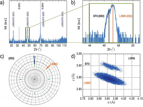
Therefore, the epitaxial relationships of the heterostructure can be resumed as LSMO (001) ║STO (001) ║Si (001) and LSMO [100] ║STO [100] ║Si [110].
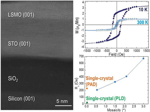
The structural quality is also reflected in the magneto-electric properties of the films. We found that non-annealed STO buffer layers modify the physical properties of PAD-derived LSMO films. This was evidenced by a degradation of the electric transport, where the metal-to-insulator transition (MIT) occurs below room temperature. Contrarily, temperature dependence of the resistivity in LSMO on 900 °C-annealed STO substrates shows a MIT around 340 K with a metallic behavior (dρ/dT> 0) ((a)). The temperature dependence of the in-plane magnetization LSMO film under an applied magnetic field of 1000 Oe shows a TC around 320 K ((b)) close to the bulk value (TC ≈ 350 K), and in good agreement with LSMO ultrathin films grown by physical methods [Citation41,Citation52,Citation53]. This result demonstrates the stoichiometric control of the films deposited by PAD on annealed STO buffer layers. Moreover, the magnetic hysteresis loops of the LSMOPAD/STOMBE/Si confirm the ferromagnetic behavior also at 300 K. Saturation of the magnetization occurs at H ≈ 1500 Oe, and the coercive field (Hc) is ≈ 200 Oe ((c)). Note that this Hc value is larger than in LSMO films obtained by PLD [Citation54] due to stress relaxation mechanism of quasi thermodynamic PAD process, and more importantly, similar to LSMO films grown on STO single crystals by PAD technique [Citation37].
Figure 4. a) Temperature dependence of the resistivity measured in N2 up to 400 K in a Van der Pauw configuration for LSMO films deposited on top of non-annealed (cyan) and annealed (blue) STO-buffered Si substrates. b) Field-cooled temperature dependence of the magnetization (Bohr magneton per atom of manganese) in an applied in-plane magnetic field of 1000 Oe for the LSMOPAD/STOMBE/Si film. c) In-plane field dependence (Bohr magneton per atom of manganese at 10 K and 300 K) of the magnetization. d) Magnetoresistance at 300 K. Data corresponds to LSMO films deposited on STO/Si substrate with a mosaicity value of 1°.
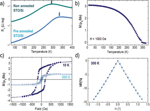
We performed a detailed characterization of the MR around the MIT (Figure S6) that showed a value greater than 10% at 1 T at room temperature ((d)). This low-field magnetoresistance (LFMR) effect in thin films can be attributed to grain boundaries [Citation55], texture [Citation56,Citation57], and epitaxial strain [Citation58]. We ascribe the enhancement of the MR to the mosaicity of the STO buffer layer, with a full width at half maximum (FWHM) larger than in a single crystal, and to the stress relaxation mechanism of the tensile strain imposed over the LSMO in PAD method [Citation37]. This result opens the possibility to tune the MR at low fields and, thus, could be useful for the development of magnetoresistive sensors at room temperature [Citation59] in silicon-based devices.
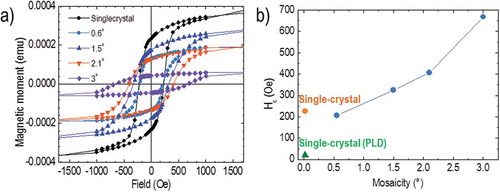
Likewise, the mosaicity of the STO layer, that is, the spreading degree of crystal plane orientations, can also modify other magnetic properties of the epitaxial LSMO layer. (a) shows the evolution of different STO-buffer layers according the FWHM values where the more misaligned (001) planes correspond to higher mosaicity samples. This feature is controlled by the Sr excess during the MBE growth at early deposition stages that produces arrays of slightly misaligned STO grains, yielding a high mosaicity [Citation44]. This phenomenon can be clearly observed through atomic-resolution Z-contrast image of two extreme cases: (0.6°), with a crystallinity close to single-crystal, and (3.0°) ((b)). While the more crystalline STO/Si film is continuous, the 3.0°-STO/Si has different domains that affect the magnetic properties of epitaxial LSMO films. Indeed, we found a direct dependence of the coercivity on the mosaicity of the STO-buffer layer (). In this case, STO buffered Si substrates with higher values of mosaicity, that is, smaller grain size and higher nanostructuration [Citation60], induce larger coercivity fields, which results from the strong dependence of the coercive field on the microstructure of the material (such as size of crystal grains and film roughness) [Citation61]. LSMO samples with mosaicity values ranging from 0.5° to 1° exhibit the optimum Hc value, which is similar to LSMO films grown on single-crystal substrates. Therefore, the mosaicity of STO/Si buffer substrate combined with PAD methodology is an effective tool to control the magnetic anisotropy in LSMO ferromagnetic thin films integrated in silicon technology.
Figure 5. a) FWHM values, obtained from rocking curves of the (002) peak of STO for STO/Si buffer layers with different mosaicity degrees. b) Atomic resolution Z-contrast image viewed along the [100]-crystallographic direction to compare two STO/Si samples with 0.6° (bottom) and 3.0° (up) FWHM values.
![Figure 5. a) FWHM values, obtained from rocking curves of the (002) peak of STO for STO/Si buffer layers with different mosaicity degrees. b) Atomic resolution Z-contrast image viewed along the [100]-crystallographic direction to compare two STO/Si samples with 0.6° (bottom) and 3.0° (up) FWHM values.](/cms/asset/78b04154-fa7f-4cd2-bcd6-bc4469409994/tsta_a_1520590_f0005_oc.jpg)
Figure 6. a) Hysteresis loops at 10 K for LSMO/STO/Si films as a function of the mosaicity from single-crystal up to FWHM of 3°. b) Evolution of the LSMO coercivity as a function of mosaicity of the STO-buffered silicon substrates.
Conclusions
The thermal and chemical stability exhibited by STO layers grown on silicon substrates by MBE allowed chemical deposition of high-quality epitaxial LSMO ultrathin films using PAD process at 950 °C in air atmosphere within 2 h on STO/Si buffer layers preannealed at 900 °C. Magnetic and electric properties of epitaxial LSMO films confirmed the compatibility between PAD and MBE processes. LSMO films with mosaicity values ranging from 0.5° to 1° exhibit the optimum Hc value, which is similar to LSMO films grown on STO single-crystal substrates and a low-field magnetoresistance effect. A precise control of the coercive field of LSMO films can be achieved by tuning the mosaicity of the STO/Si buffer layer. Our growth strategy demonstrates the enormous potential of combining physical and chemical processes for the development of low-cost functional oxide-based devices compatible with standard microfabrication technologies on silicon substrates.
Supplemental Material
Download MS Word (2.6 MB)Acknowledgments
ACG acknowledges the financial support from the French Agence Nationale pour la Recherche (ANR), project Q-NOSS ANR-16-CE09-0006-01 and École Centrale de Lyon under the BQR 2016 project. The research leading to these results has received funding from the European Union Seventh Framework Program under Grant Agreement 312483 - ESTEEM2 (Integrated Infrastructure Initiative–I3). This project has received funding from the EU‐H2020 research and innovation Program under grant agreement No 654360 having benefitted from the access provided by ICMAB-CSIC in Barcelona within the framework of the NFFA‐Europe Transnational Access Activity. Fruitful discussions with Pr. F. Rivadulla from USC are highly acknowledged. INL authors acknowledge the European Commission for funding the project TIPS (H2020-ICT-02-2014-1-644453). We thank P. Regreny, C. Botella, and J. B. Goure for the MBE technical assistance on the Nanolyon technological platform. The HRTEM microscopy work was conducted in “Laboratorio de Microscopías Avanzadas” at the Instituto de Nanociencia de Aragón-Universidad de Zaragoza. Authors acknowledge the LMA-INA for offering access to their instruments and expertise.
Disclosure statement
No potential conflict of interest was reported by the authors.
Supplementary material
Supplementary data can be accessed here.
Additional information
Funding
Related Research Data
References
- Goodenough JB. Electronic and ionic transport properties and other physical aspects of perovskites. Rep Prog Phys. 2004;67(11):1915–1993.
- Dagotto E , Hotta T , Moreo A. Colossal magnetoresistant materials: the key role of phase separation. Physics Report. 2001;344(1–3):1–153.
- Von Helmolt, R. , Wecker J , Holzapfel B , et al. Giant negative magnetoresistance in perovskitelike La2/3Ba1/3MnOx ferromagnetic films. Phys Rev Lett. 1993;71(14):2331–2333.
- Ramirez AP . Colossal magnetoresistance. J Phys Condensed Matter. 1997;9(39):8171–8199.
- Hwang, HY , Cheong SW , Ong NP , et al. Spin-polarized intergrain tunneling in La2/3Sr1/3MnO3 . Phys Rev Lett. 1996;77(10):2041–2044.
- Schiffer, P , Ramirez AP , Bao W , et al. Low temperature magnetoresistance and the magnetic phase diagram of La1-xCaxMnO3 . Phys Rev Lett. 1995;75(18):3336–3339.
- Prellier W , Lecoeur P , Mercey B . Colossal-magnetoresistive manganite thin films. J Phys Condensed Matter. 2001;13(48):R915–R944.
- Demkov AA , Posadas AB . Integration of functional oxides with semiconductors. New York: Springer, 2014.
- Reiner JW , Kolpak AM , Segal Y , et al. Crystalline oxides on silicon. Adv Mater. 2010;22(26–27):2919–2938.
- Baek SH , Eom CB . Epitaxial integration of perovskite-based multifunctional oxides on silicon. Acta Mater. 2013;61(8):2734–2750.
- Vila-Fungueirino, JM , Bachelet R , Saint-Girons G , et al. Integration of functional complex oxide nanomaterials on silicon. Front Phys. 2015;3:12.
- Schlom, DG , Chen LQ , Pan X , et al. A thin film approach to engineering functionality into oxides. J Am Ceramic Soc. 2008;91(8):2429–2454.
- McKee RA , Walker FJ , Chisholm MF . Crystalline oxides on silicon: the first five monolayers. Phys Rev Lett. 1998;81(14):3014–3017.
- Wang J , Zheng H , Ma Z , et al. Epitaxial BiFeO3 thin films on Si. Appl Phys Lett. 2004;85(13):2574–2576.
- Baek SH , Park J , Kim DM , et al. Giant piezoelectricity on Si for hyperactive MEMS. Science. 2011;334(6058):958–961.
- Abel S , Stöferle T , Marchiori C , et al. A strong electro-optically active lead-free ferroelectric integrated on silicon. Nat Commun. 2013;4.
- Moalla R , Vilquin B , Saint-Girons G , et al. Huge gain in pyroelectric energy conversion through epitaxy for integrated self-powered nanodevices. Nano Energy. 2017;41:43–48.
- Sánchez F , Aguiar R , Trtik V , et al. Epitaxial growth of SrTiO3 (00h), (00h), and (hhh) thin films on buffered Si(001). J Mater Res. 1998;13(6):1422–1425.
- Narayan J , Larson BC . Domain epitaxy: a unified paradigm for thin film growth. J Appl Phys. 2003;93(1):278–285.
- Tiwari A , Chug A , Jin C , et al. Integration of single crystal La0.7Sr0.3MnO3 films with Si(001). Solid State Commun. 2002;121(12):679–682.
- Carretero-Genevrier A , Drisko GL , Grosso D , et al. Mesoscopically structured nanocrystalline metal oxide thin films. Nanoscale. 2014;6(23):14025–14043.
- Xia Y , Whitesides GM . Soft lithography. Annu Rev Mater Sci. 1998;28(1):153–184.
- Brinker CJ , Lu Y , Sellinger A , et al. Evaporation-induced self-assembly: nanostructures made easy. Advanced Mater. 1999;11(7):579–585.
- Lange FF . Chemical solution routes to single-crystal thin films. Science. 1996;273(5277):903–909.
- Schwartz RW , Schneller T , Waser R . Chemical solution deposition of electronic oxide films. Comptes Rendus Chimie. 2004;7(5):433–461.
- Calzada ML , Bretos I , Jiménez R , et al. Low-temperature processing of ferroelectric thin films compatible with silicon integrated circuit technology. Advanced Mater. 2004;16(18):1620–1624.
- Vila-Fungueiriño JM , Rivas-Murias B , Rivadulla F . Synthesis and magnetic properties of manganite thin films on Si by polymer assisted (PAD) and pulsed laser deposition (PLD). 2012 MRS Spring Meeting;. San Francisco, CA. 2012.
- Carretero-Genevrier A , Gich M , Picas L , et al. Soft-chemistry-based routes to epitaxial α-quartz thin films with tunable textures. Science. 2013;340(6134):827–831.
- Carretero-Genevrier A , Puig T , Obradors X , et al. Ferromagnetic 1D oxide nanostructures grown from chemical solutions in confined geometries. Chem Soc Rev. 2014;43(7):2042–2054.
- Carretero-Genevrier A , Oro-Sole J , Gazquez J , et al. Direct monolithic integration of vertical single crystalline octahedral molecular sieve nanowires on silicon. Chem Mater. 2014;26(2):1019–1028.
- Jia QX , McCleskey TM , Burrell AK , et al. Polymer-assisted deposition of metal-oxide films. Nat Mater. 2004;3(8):529–532.
- Burrell AK , Mark McCleskey T , Jia QX . Polymer assisted deposition. Chem Communications. 2008;11:1271–1277.
- Vila-Fungueirino JM , Rivas-Murias B , Rubio-Zuazo J , et al. Polymer assisted deposition of epitaxial oxide thin films. J Mater Chem C. 2018;6(15):3834–3844.
- Vila-Fungueiriño JM , Rivas-Murias B , Rodríguez-González B , et al. Interface magnetic coupling in epitaxial bilayers of La0.92MnO3/LaCoO3 prepared by polymer-assisted deposition. Chem Mater. 2014;26(3):1480–1484.
- Jain, M. , Hundley MF , Hawley M , et al. Magnetoresistance in polymer-assisted deposited Sr- and Ca-doped lanthanum manganite films. Appl Phys Lett. 2006;88(23):232510.
- Jain M , Bauer E , Ronning F , et al. Mixed-valence perovskite thin films by polymer-assisted deposition. J Am Ceramic Soc. 2008;91(6):1858–1863.
- Vila-Fungueiriño JM , Bui CT , Rivas-Murias B , et al. Thermodynamic conditions during growth determine the magnetic anisotropy in epitaxial thin-films of La0.7Sr0.3MnO3 . J Phys D Appl Phys. 2016;49(31):315001.
- Jain M , Shukla P , Li Y , et al. Manipulating magnetoresistance near room temperature in La0.67Sr0.33MnO3/La0.67Ca0.33MnO3 films prepared by polymer assisted deposition. Advanced Mater. 2006;18(20):2695–2698.
- Lucas I , Vila-Fungueiriño JM , Jiménez-Cavero P , et al. Tunnel conduction in epitaxial bilayers of ferromagnetic LaCoO3/La2 / 3Sr1 / 3MnO3 deposited by a chemical solution method. ACS Appl Mater Interfaces. 2014;6(23):21279–21285.
- Vila-Fungueiriño JM , Rivas-Murias B , Rodríguez-González B , et al. Room-temperature ferromagnetism in thin films of LaMnO3 deposited by a chemical method over large areas. ACS Appl Mater Interfaces. 2015;7(9):5410–5414.
- Méchin L , Adamo C , Wu S , et al. Epitaxial La0.7Sr 0.3MnO3 thin films grown on SrTiO3 buffered silicon substrates by reactive molecular-beam epitaxy. Phys Status Solidia. 2012;209(6):1090–1095.
- Le Bourdais D , Agnus G , Maroutian T , et al. Epitaxial manganite freestanding bridges for low power pressure sensors. J Appl Phys. 2015;118(12):124509.
- Adamo, C , Méchin, L , Heeg, T , et al. Enhanced electrical and magnetic properties in La0.7Sr0.3MnO3 thin films deposited on CaTiO3-buffered silicon substrates. APL Materials. 2015;3(6):062504.
- Saint-Girons G , Bachelet R , Moalla R , et al. Epitaxy of SrTiO3 on silicon: the knitting machine strategy. Chem Mater. 2016;28(15):5347–5355.
- Delhaye, G , Merckling, C , El-Kazzi, M , et al. Structural properties of epitaxial SrTiO3 thin films grown by molecular beam epitaxy on Si(001). J Appl Phys. 2006;100(12):124109.
- Park, JW , Baek, SH , Bark, CW , et al. Quasi-single-crystal (001) SrTiO3 templates on Si. Appl Phys Lett. 2009;95(6):061902.
- Kawasaki M , Takahashi K , Maeda T , et al. Atomic control of the SrTiO3 crystal surface. Science. 1994;266(5190):1540–1542.
- Qiao L , Zhang KHL , Bowden ME , et al. The impacts of cation stoichiometry and substrate surface quality on nucleation, structure, defect formation, and intermixing in complex oxide heteroepitaxy-LaCrO3 on SrTiO3(001). Adv Funct Mater. 2013;23(23):2953–2963.
- Niu G , Yin S , Saint-Girons G , et al. Epitaxy of BaTiO3 thin film on Si(0 0 1) using a SrTiO3 buffer layer for non-volatile memory application. Microelectron Eng. 2011;88(7):1232–1235.
- Zhang Y , Yan Q , Yang F , et al. Oxygen pressure dependence of dielectric properties in SrTiO3/Si heterojunctions. Ceramics Int. 2016;42(11):12672–12674.
- Seifert A , Vojta A , Speck JS , et al. Microstructural instability in single-crystal thin films. J Mater Res. 1996;11(6):1470–1481.
- Perna P , Méchin L , Chauvat MP , et al. High Curie temperature for La0.7Sr0.3MnO3 thin films deposited on CeO2/YSZ-based buffered silicon substrates. J Phys Condens Matter. 2009;21(30):306005.
- Pradhan AK , Dadson JB , Hunter D , et al. Ferromagnetic properties of epitaxial manganite films on SrTiO3/Si heterostructures. J Appl Phys. 2006;100(3):033903.
- Boschker H , Huijben M , Vailionis A , et al. Optimized fabrication of high-quality La0.67Sr0.33MnO3 thin films considering all essential characteristics. J Phys D Appl Phys. 2011;44(20):205001.
- Gupta A , Gong G . Grain-boundary effects on the magnetoresistance properties of perovskite manganite films. Phys Rev B Condensed Matter Mater Phys. 1996;54(22):R15629–R15632.
- Teo BS , Mathur ND , Isaac SP , et al. Low field magnetotransport in La0.7Sr0.3MnO3 films. J Appl Phys. 1998;83(11):7157–7159.
- Walter T , Dörr K , Müller K-H , et al. Low-field magnetoresistance of La0.7Sr0.3MnO3 thin films with gradually changed texture. Appl Phys Lett. 1999;74(15):2218–2220.
- O’Donnell J , Onellion M , Rzchowski MS , et al. Low-field magnetoresistance in tetragonalsfilms. Phys Rev B Condensed Matter Mater Phys. 1997;55(9):5873–5879.
- Balcells L , Carrillo AE , Martı́nez B , et al. Room temperature magnetoresistive sensor based on thick films manganese perovskite. J Magn Magn Mater. 2000;221(1–2):224–230.
- Gómez A , Vila-Fungueiriño JM, Moalla R. Electric and mechanical switching of ferroelectric and resistive states in semiconducting BaTiO3 – δ films on silicon. Small. 2017;13(39):1701614.
- Arzt E . Size effects in materials due to microstructural and dimensional constraints: a comparative review. Acta Mater. 1998;46(16):5611–5626.