
 ?Mathematical formulae have been encoded as MathML and are displayed in this HTML version using MathJax in order to improve their display. Uncheck the box to turn MathJax off. This feature requires Javascript. Click on a formula to zoom.
ABSTRACT
We report large amplitude modulation waveforms as large as ~ 10 V using vanadium dioxide micro-channel devices operating under current-controlled conditions. The self-sustained electrical oscillations were generated by controlling the applied current in the negative differential resistance region of the investigated devices. An appropriate value of internal capacitance was achieved as parasitic capacitance in the device structure to stabilize the electrical oscillations. This eliminates the need of an external pulsed source or any external passive component connected to the micro-channel devices. Amplitude and frequency of the oscillation were tuned by illuminating the device micro-channel with an external laser. An equivalent circuit model was developed to simulate the waveforms. A good agreement between experiment and simulation was verified.
Graphical Abstract
1. Introduction
Novel electronic switches, memristive systems and oscillators are critical components for a variety of tunable electronics applications. Transition metal oxides are promising candidates in realizing such devices. Among the various transitional metal oxides, stoichiometric vanadium dioxide (VO2) is receiving considerable attention due to its marked and reversible insulator-to-metal phase transition (IMT) [Citation1]. Pronounced changes in electro-optical properties across the IMT is a signature of this process. Below the IMT temperature, VO2 exhibits a monoclinic crystal structure [Citation2,Citation3] with a ~ 0.7 eV energy band-gap [Citation4,Citation5] and high electrical resistivity (the insulator state). In contrast, beyond the phase transition, VO2 exhibits a rutile structure, with no band-gap and very high electrical conductivity (the metallic state) [Citation2,Citation3]. The IMT in VO2 can be triggered by the application of an external electric field, heat or an optical excitation. Such tunable capability can be exploited for designing microelectronic and optoelectronic devices beyond CMOS technology with reconfigurable characteristics [Citation6]. VO2-based terahertz modulators [Citation7,Citation8], analogue modulators [Citation9], tunable meta-materials [Citation10,Citation11], field-effect transistors [Citation12–Citation14] and memristors [Citation15,Citation16] have been already demonstrated.
Two-terminal electrical devices incorporating VO2 micro-channels are of particular interest due to their spontaneous electrical oscillation characteristics [Citation17–Citation21]. These devices exhibit well-pronounced negative differential resistance (NDR) [Citation17,Citation18], an essential attribute for practical realization of electrical oscillators. Such oscillators do not require inductive components to generate the waveforms. This can be potentially used to fabricate tunable micro- or nano-oscillators for a variety of applications spanning from analogue electronics to artificial neural networks [Citation19]. Under specific biasing conditions, the two-terminal device resistance spontaneously oscillates between the insulating and the metallic states. The dynamics of the phase transition in two-terminal VO2 devices is different under voltage controlled (VC) or current controlled (CC) modes of operation [Citation22,Citation23]. The VC phase transition exhibits a much larger hysteresis loop width when compared to the CC mode of operation. Also, under CC operation conditions less Joule heating is generated making this mode of operation more attractive than the VC one [Citation17,Citation24].
VO2 oscillators, excited by voltage actuation [Citation18,Citation25] or current actuation [Citation24] have been reported. However, the generation of electrical oscillations with such devices requires an external current or voltage pulse source and an external resistive component connected to the device. Voltage actuation with a DC voltage still requires an external resistive component to generate the oscillations [Citation17]. A combination of an external resistor in parallel with a capacitor is required in the relaxation oscillation experiments [Citation26]. In this work, we show that electrical oscillations under current actuation in VO2 two-terminal devices can be achieved using only the internal capacitance of the investigated devices, thus eliminating the need of an external current pulse source or any passive external electrical component. We demonstrate very stable oscillation waveforms for over millions of cycles without any significant performance degradation. This reduction in the complexity of the oscillator circuit is significant for prospective large-scale integration and fabrication of micro- or nano-oscillators in a single chip. In order to validate our experimental results, we developed an equivalent circuit model and compared the simulated results with measured self-oscillation. We have also investigated the effects of the optical power excitation from an external laser illuminating the device micro-channels on the frequency and amplitude of the oscillations.
2. Experiments
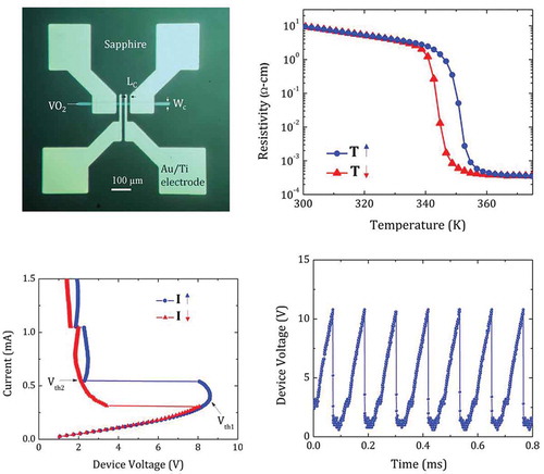
Planar VO2 micro-channel devices investigated here were fabricated using conventional photolithography, plasma etching, electron-beam metal deposition and lift-off techniques. First VO2 films ~ 130 nm thick were deposited on c-plane (0001) oriented sapphire substrates using the reactive DC magnetron sputtering technique [Citation27]. Then the VO2 films were patterned into long straight line-shapes (~ 400–500 μm length) with 10 µm or 20 µm in width by plasma etching following the first lithography step. Next, a second lithography step was performed followed by the deposition of 100/20-nm-thick Au/Ti layers using the electron-beam deposition technique. Finally, the electrodes were defined using a lift-off procedure in acetone. ) shows a representative optical microscope image of a VO2 device with 20-µm channel length (LC ) and 20-µm channel width (WC ). The device design layout is similar to that previously reported by Sakai et al. [Citation17,Citation28]. The width of the electrodes was designed to be much larger than the width of VO2 lines to provide a uniform electric field across the channel region and to prevent any delayed phase transition outside of the electrode region [Citation17,Citation18].
Figure 1. Optical microscope image of a D20 VO2 micro-channel device. (b) The change in VO2 resistivity for increasing and decreasing temperatures.
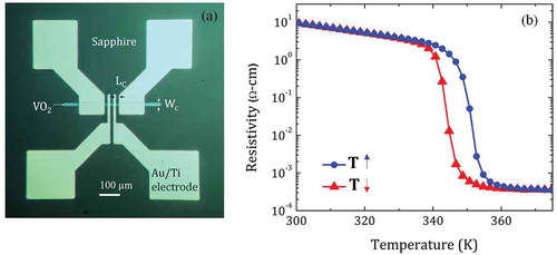
After sample fabrication, the entire chip was housed inside a ceramic package and wire-bonded in order to perform the electrical characterization experiments. The package was then placed over a thermoelectric heater/cooler controlled stage for varying the temperature (Ts ). A computer-controlled DC power source was used to provide power and to monitor the current and the voltage across the devices. A 0–5 kΩ potentiometer was used as an external load resistor (Rext ). A digital oscilloscope was used for recording the electrical oscillation waveforms. Two adjacent electrodes were used in our experiments. The change in resistivity during the IMT is depicted in ) for increasing and decreasing temperatures (T). Such measurements were performed for a VO2 thin film grown under similar conditions. Since the VO2 micro-channels used in our experiments exhibited a relatively high resistance at room temperature (~ 150 kΩ), all the experiments were performed at stage temperatures in the range 50 < TS < 65 °C, which is still lower than the VO2 phase transition temperature [Citation9], during CC or VC mode of operation. This procedure was used to reduce the switching threshold voltage to achieve the IMT, preventing electrical breakdown of the devices. Similar experiments can be performed at room temperature using low resistivity VO2 material [Citation17,Citation18]. Measured phase transition temperatures of 342 K and 352 K (see )) were determined for heating and cooling cycles, respectively. However, there is a ~ 10 oC temperature offset in TS where TS < T due to the thermal impedance of the ceramic package and the heating stage. The total current (ISP ) in the circuit and the voltage drop (Vchannel ) in the micro-channel devices can be simply determined using Ohms’ law relations:
where Rchannel is the device resistance, which is essentially the resistance of the VO2 channel, and VSP is the voltage supplied by the DC power source. The Rchannel of each device was measured using a digital ohmmeter at different device temperatures.
The oscillation waveform frequency and amplitude can be varied using an external laser illuminating the devices. We have used a fibre-coupled continuous-wave 980 nm wavelength semiconductor laser diode as the optical excitation source operating at different power levels (Po ). The laser output from the multimode optical fibre was placed near the top of the VO2 micro-channel region of the devices with a ~ 300 μm beam diameter.
3. Results
3.1 I–V characteristics and electrical oscillations
The current-voltage (I–V) curves of a 10 µm × 10 µm device (denoted as D10) and a 20 µm × 20 µm device (denoted as D20) in the VC mode of operation are shown in and , respectively. The results shown in were obtained with fixed external resistor Rext = 4 kΩ and Ts = 64 °C. The I–V curves were acquired by applying an increasing or decreasing voltage (or current) to the circuit. The external resistor was used to prevent an electrical breakdown when the micro-channel device was in the highly conductive state. The insets in show the corresponding I–V curves for the total voltage drop in the circuit. Initially, the channel is in the insulating state with very high resistance. When the device voltage reaches the forward threshold voltage (Vth1 ), the IMT occurs and the device current increases. The NDR region is clearly visible after Vth1 is reached for both devices. Such anomalous behaviour is due to the increase in channel conductivity and simultaneous decrease in the voltage drop across the channel. The higher IMT threshold voltage and larger width of the NDR region in the device D20, when compared to the device D10, is attributed to differences in the VO2 channel dimensions. The IMT threshold voltage is higher for larger separation between the two electrodes and it is lower for wider channels. When the VO2 transforms into the metallic state the voltage drop in the channel does not increase significantly with further increase in the current due to its low resistance (~ 400 Ω). The reverse IMT process occurs when the voltage is decreased. The backward threshold voltage (Vth2 ) is lower than Vth1 but similar NDR behaviour can be observed for both devices. The I–V curves for the total voltage drop in the circuit exhibits well-defined switching characteristics (see the insets in ) during the IMT and clear contrast between the metallic and insulating states is observed accompanied by large hysteresis loop widths for both devices. The device I–V curves under CC mode of operation are shown in and for the same devices D10 and D20, respectively. In the VC mode of operation, the voltage is continuously increased (or decreased) while the current is determined by the applied voltage in the device. In contrast, in the CC mode of operation, the current is increased (or decreased) continuously and the voltage drop in the device depends on the magnitude of the applied current. These curves revealed hysteresis loop widths narrower than those obtained under VC mode of operation (see ). Due to differences in VO2 micro-channel dimensions the device D10 ()) exhibited a smaller hysteresis than the device D20 ()). The ‘S’ NDR shapes observed in is a signature of VO2 two-terminal micro-channel devices [Citation17]. Initially, the channel is in the insulator state and when a threshold current is reached, the channel conductivity starts to rise at the onset of the phase transition and the IMT occurs when the current is further increased. The points Vth1 and Vth2 (see and ) represents the two threshold voltages for the forward and the backward phase transition, respectively, similar to the VC mode of operation (see ). The devices exhibited infinite differential resistance between Vth1 and Vth2 for increasing (or decreasing) currents. In the CC mode of operation, the current is restricted and that is why the current does not increase sharply at Vth1 ; instead, the voltage drops since it is not controlled in the CC mode of operation. Thus, infinite NDR is observed.
Figure 2. I–V curves for devices D10 (a) and D20 (b) under VC mode of operation at increasing (•) or decreasing (▲) device voltage. The insets show the corresponding I–V curves at increasing or decreasing total voltage in the circuit. Measurements were performed with fixed Rext = 4.0 kΩ and TS = 64 °C for both devices. Points Vth1 and Vth2 are the threshold voltages corresponding to the forward and the reverse IMT, respectively.
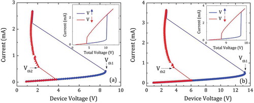
Figure 3. I-V curves for devices D10 (a) and D20 (b) under CC mode of operation at increasing (•) or decreasing (▲) device current. Measurements were performed with fixed Rext = 4.0 kΩ and TS = 64 °C. Points Vth1 and Vth2 are the threshold voltages corresponding to the forward and the reverse IMT, respectively.
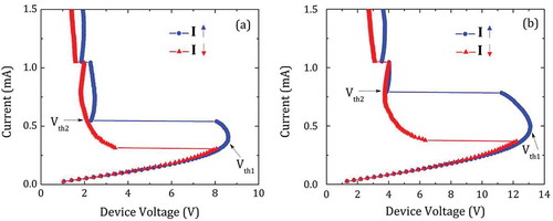
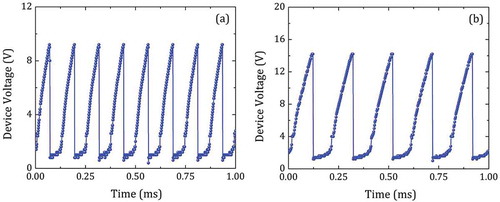
The current ‘jumps’ after the phase transition around 1 mA, in the I–V curves shown in ) and ( are possibly associated with additional transformation of a fraction of VO2 domains into the metallic state as the current is further increased. The differences in voltages for increasing and decreasing currents after the IMT, is attributed to reduced hysteresis effect since less heat is generated under CC mode of operation. and show the electrical oscillation waveforms for devices D10 and D20, respectively. An external resistor, Rext = 1.5 kΩ in series with the devices was used in these experiments. The circuit was biased with Isp = 0.8 mA and the measurements were carried out at TS = 64 °C. Large modulation voltages (ΔVPP ≈ 13 V, 8.6 V) were observed for both devices. We determined waveform oscillation frequencies fo ≈ 8.3 kHz and fo ≈ 5 kHz for devices D10 and D20, respectively (see , ). The difference in oscillation frequency is attributed to the differences in the channel dimensions on the two devices. Each cycle of oscillation consists of an exponential voltage build-up across the channel followed by a rapid (~ 1 μs) relaxation when threshold voltage for IMT is reached.
Figure 4. Electrical oscillation waveforms obtained under CC mode of operation for devices D10 (a) and D20 (b). Measurements were obtained at fixed ISP = 0.8 mA, Rext = 1.5 kΩ and TS = 64 °C.
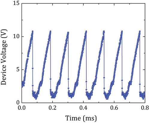
The electrical oscillation waveforms in VO2 micro-channel devices can also be obtained without any external series resistance. shows the spontaneous oscillation between the insulator and metallic states for a device D10 using Isp = 0.6 mA and Ts = 60 °C without an external series resistance. Such oscillation is triggered for ISP ≥ 0.6 mA. ISP = 0.6 mA is sufficient to induce the IMT but neither insulating nor metallic states are stabilized and hence oscillations are observed. Any lower ISP is unable to induce the IMT and the VO2 channel remains permanently in the insulating state and no oscillations are observed. For very large ISP the channel transforms permanently into the metallic state and no oscillations are observed either. We determined ΔVPP ≈ 10 V and fo ≈ 9.1 kHz from the waveform shown in . Both and depict CC mode of oscillation. However, the exponentially rising part of the oscillation waveform is steeper (see ) in this configuration when compared to the oscillation waveforms generated with the external resistor shown in due to a reduced time constant. The higher oscillation frequency is attributed to a faster exponential voltage build-up across the channel. The result shown in indicates that the complexity of prospective oscillator circuits incorporating VO2 micro-channels can be further reduced by eliminating the need of using external resistors connected to the devices.
Figure 5. Electrical oscillation waveform obtained under CC mode of operation for a D10 device without any external series resistance. The measurement was carried out at fixed ISP = 0.6 mA and TS = 60 °C.
3.2 Effect of an external optical excitation on the oscillation waveforms
Fine tuning of the frequency and the peak-to-peak amplitude of the oscillation waveforms under CC mode of operation was achieved using an external optical excitation source to illuminate the VO2 channels of the devices. A similar voltage and frequency tuning could be also achieved by changing the device temperature. However, using an external laser source, the additional photo-induced heating can be realized at localized regions of the device and this provides further control over the oscillation waveforms. Furthermore, the localized photo-induced heating process can be accomplished much faster than the thermal tuning, which requires heating and temperature stabilization of the entire device package.
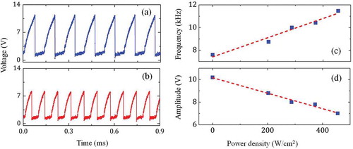
and show, respectively, generated waveforms for a D10 device obtained without any external laser (Po = 0) and with a laser excitation power Po ≈ 455 W/cm2. In these experiments we have used fixed ISP = 1 mA, Rext = 1.5 kΩ and Ts = 60 °C. At Po = 0 ()) and Po ≈ 455 W/cm2 ()), we determined, respectively, fo ≈ 7.6 kHz and fo ≈ 11.5 kHz. The change in oscillation frequency is accompanied by changes in ΔVPP . At Po ≈ 455 W/cm2 ()), we determined a reduction in ΔVPP by 3.2 V when compared to the case of no laser illumination ()). The oscillation waveform ceased to exist for Po > 455 W/cm2. The observed changes in fo and ΔVPP with increasing laser power were attributed to changes in threshold voltages Vth1 and Vth2 as discussed in section 3.1.
Figure 6. Electrical oscillation waveforms obtained under CC mode of operation for a D10 device at fixed ISP = 1 mA, Rext = 1.5 kΩ and TS = 60 °C. (a) no laser illumination and (b) illuminated by a laser with Po ≈ 455 W/cm2. (c) Measured oscillation frequencies and (d) peak-to-peak amplitude voltage for a D10 device at different laser power densities. The dashed straight lines in (c) and (d) are guides to the eye.
4. Discussions
4.1 Oscillation mechanism and the origin of exponential nature of the waveforms
The origin of the electrical oscillation waveforms shown in is revealed through a careful observation of the I–V curves under CC mode of operation shown in . Before reaching the IMT threshold voltage Vth1 the channel has high resistance. During the phase transition, the channel conductivity increases and the voltage drop across channel decreases simultaneously creating the NDR region. The current rises after Vth1 is reached and the current at this voltage is Ith1 . When biased by a constant current higher than Ith1 the device voltage oscillates between the voltages Vth1 and Vth2 . The value of this current (Isp > Ith1 ) is the threshold current required to trigger the oscillation. If supplied by a current lower than Ith1 , the device does not oscillate.
Initially the channel is in the insulating state and the voltage across the device increases when supplied by an external current source. This is characterized by the exponentially increasing part of the oscillation waveforms (see , and ). Such voltage build-up is cut-off by the IMT and is marked by the peaks of the waveforms. After the IMT the VO2 channel transforms into the metallic phase with very low resistance and the channel voltage drops abruptly (beyond Vth2 ) similar to previous reports [Citation17,Citation18]. Then the channel voltage increases again and the process is repeated cyclically. The exponential build-up of voltage across the micro-channel is analogous to the electrical response of an RC circuit. The two Au/Ti electrodes of the device act as capacitor providing the effective internal capacitance (Cosc ). The physical equivalent circuit for the device comprises of a parallel combination of the channel resistance and the effective capacitance (see inset of )). The exponentially rising region of the waveforms can be fitted with the following empirical exponential RC circuit charging relation [Citation17]:
Figure 7. Nonlinear square fittings of the exponential part of the voltage build-up in the VO2 micro-channel for one oscillation cycle for: (a) device D10: ISP = 1 mA and ISP = 0.6 mA with fixed TS = 60 °C and Rext = 1.5 kΩ. The inset shows the schematic of the physical equivalent circuit for the VO2 micro-channel devices. (b) Device D10: Rext = 0 Ω and Rext = 1.5 kΩ with fixed ISP = 0.6 mA and TS = 60 °C.
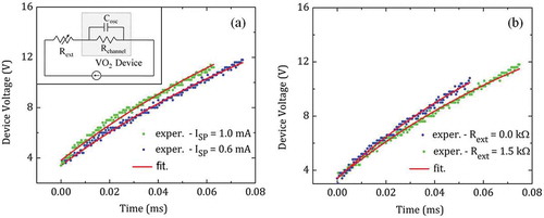
where ΔVM0 is the target voltage modulation which is controlled by the voltage supplied by the current source to drive the constant current in the circuit and it is cut off by the phase transition at Vth1. τ is the characteristic time constant of the equivalent RC circuit, and to is a time-reference shifting parameter for the oscillation time scale. During such exponential voltage build-up, charges appear on the large electrodes whereas a small current flows through the highly resistive VO2 channel. When the voltage across the channel is larger than Vth1 , the channel transforms into the metallic state and the charges rapidly flow through the channel whereas the source voltage is reduced to maintain a constant current in the circuit. In ) we show the non-linear square fitting using (3) for the oscillation waveforms for a D10 device with ISP = 1 mA and ISP = 0.6 mA during the exponential voltage build-up, at TS = 60 °C. We determined an identical time constant τ = 135.7 µs for both curves but the target voltage modulation is higher for ISP = 1 mA. Thus voltage rises faster for ISP = 1 mA and a higher oscillation frequency is observed when compared to ISP = 0.6 mA. The effect of the external resistance on the oscillation waveform is shown in ) for the same device with ISP = 0.6 mA and TS = 60 °C. The target voltage modulation is identical for both curves but the time constant decreased from 113.4 µs to 98.9 µs for the measurements with Rext = 1.5 kΩ and no external resistor, respectively. The oscillation frequency increased from fo ≈ 7.7 to 9.1 kHz due to a decrease in the time constant when the external resistor is removed. A direct measurement of the devices’ capacitance yielded a value of ~ 10−12 F. However, an effective capacitance of ~ 10−9 F was determined from the non-linear square fitting of the experimental data. This is attributed to the relatively slow time response (~ 100 µs) and output capacitance (~ 10−9 F) of the power source under the CC mode of operation. This also limited the frequency of the oscillations in our experiments to ~ 10 kHz.
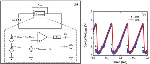
The S-type I–V curves exhibited by the two-terminal VO2 devices (see ) are characterized by the two threshold voltages Vth1 and Vth2 corresponding to the forward and reverse IMT, respectively. When the device is supplied by a constant current, higher than the aforementioned threshold current, the corresponding voltage across the device cannot increase instantaneously. Instead, it rises exponentially similar to a capacitor charging (see – and ). After Vth1 is reached, the VO2 channel transforms into the metallic state creating a current flow path parallel to the internal capacitor (see inset of )). A rapid relaxation of the capacitor charge occurs through the highly conductive channel. As a result, the voltage across the channel becomes lower than Vth2 , which is not sufficient to hold it in the metallic state since the current magnitude is limited. As the voltage across the channel drops below Vth2 , the reverse IMT occurs and the channel transforms back into the insulating state. This process is repeated to keep the current constant and then the oscillation is observed. The DC power source supplies a constant current while the voltage changes to drive the same current through the changing channel resistance. Therefore, the oscillation is a consequence of charging and discharging of the internal capacitor due to changes in the VO2 channel resistance. Such oscillation can be modelled using an equivalent circuit approach. We implemented an equivalent circuit model using the SPICE simulation software to model the observed oscillation waveforms in our experiments. ) shows the circuit equivalent model used to generate the oscillatory response under similar biasing conditions [Citation22]. The VO2 micro-channel device is represented by the voltage-controlled resistor Rchannel , which is a function of the voltage drop (Vchannel ) across the channel. The state of the device (insulator or metallic) is controlled by an ideal op-amp and it is stored inside the output capacitor (Co ). The voltage (V+ ) at the non-inverting terminal is the sum of two dependent voltage sources represented by the following relation [Citation26]:
Figure 8. (a) Equivalent circuit model for the VO2 micro-channel devices. (b) Simulated and experimental waveforms for a D10 device with ISP = 0.6 mA, Rext = 0 Ω, and Ts = 60 °C.
where Vo
is the output voltage of the op-amp. is a dimensionless parameter that represents the magnitude of VO
. The voltage at the inverting terminal is provided by another voltage dependent voltage source V ̶
= Vchannel
, that represents the voltage drop across the VO2 device. The channel resistance is controlled by the following relation [Citation26]:
where RI
and RM
represent the channel resistances in the insulating and in the metallic states, respectively, and VC
is the voltage drop across Co
. is another dimensionless parameter that represents the magnitude of VC
. Initially,
= 1 and
= 0 when Vo
= 1 V and VC
= 0 V. The device is in the insulator state and the channel resistance is RI. V+
= Vth1
is the threshold voltage to induce the IMT. When an increasing voltage is applied to the device and the voltage across the channel resistance (Rchannel
) exceeds Vth1
the op-amp output changes to 0 V and this triggers the resistance switching. In this state, the aforementioned parameters take the values
= 0 and
= 1. The channel resistance changes to Rchannel
= RM
. In the metallic state, the voltage at the non-inverting terminal becomes V+
= Vth2
and the reverse IMT occurs at a lower threshold voltage thus simulating the hysteresis effect in VO2. Discharging of the internal capacitor reduces the voltage drop across the Rchannel
. When Vchannel
drops below Vth2
the op-amp output becomes 1 V again and the capacitor voltage becomes VC
= 0 V. Thus, the reverse resistance switching occurs and the channel resistance becomes RI
again. This process is repeated and produces the voltage oscillation. A comparison between the oscillation waveform generated from the simulation and experiment for the device D10 using ISP
= 0.6 mA is shown in ). In this simulation, the metallic and insulating state resistances used were RM
≈ 400 Ω and RI
≈ 50 kΩ, respectively and the threshold voltages used were Vth1 ≈ 10.7 V and Vth2 ≈ 2.8 V. These values were determined experimentally. The product RoCo
= τo
is the time constant of the RC circuit in the output of the op-amp (see )). τo
works as a fitting parameter for the time scale of the oscillation waveform generated by the simulation. The forward and reverse switching between insulating and metallic states in the channel are not instantaneous but it rather depends on the device dimensions. τo
was chosen appropriately to take this into account and to accurately reproduce the experimental oscillation waveforms. The effective internal capacitance of the oscillator was chosen as Cosc
≈ 10−9 F. A good agreement between simulation and experimental results is evident from ). Such simplified model does not rely on first principles but it successfully provides a good description of the electrical oscillation characteristics of VO2 micro-channel devices and it can be used to predict the amplitude and frequency of the waveforms.
4.2 Optical tuning
The external optical excitation changes the transition voltage threshold by reducing the VO2 channel resistance. The frequency of the oscillation increases and the peak-to-peak voltage decreases due to the reduction of the threshold voltage. The influence of the optical excitation on the oscillation frequency was shown in . The oscillation frequency fo ≈ 7.6 kHz is observed in device D10 without optical excitation ()) and under optical illumination with Po ≈ 455 W/cm2, it increases to fo ≈ 11.4 kHz ()). The oscillation ceases to occur for Po > 455 W/cm2. Such optical power density further heats the device and transform the VO2 channel into the metallic state and therefore the oscillations were no longer observed. The exponential part of voltage build-up across the channel controls the oscillation frequency and can be approximately described by the following empirical relation.
where τ is the characteristic time constant for exponential voltage rise. The voltage rise is cut off when ΔVchannel(t) reaches the threshold voltage, Vth1 . The external optical illumination reduces the voltage rise time by lowering Vth1 . Thus, an increased oscillation frequency was observed. A linear dependence in the oscillation frequency with the optical power density was determined from ). At elevated temperatures, only a part of the resistance hysteresis loop is accessed under varying optical excitation conditions where such dependence is linear. The peak-to-peak voltage was reduced by photo-exciting the device micro-channel and a voltage peak-to-peak amplitude change from 10.2 V to 7.0 V (see )) was determined when the laser power density was varied from Po ≈ 0 to Po ≈ 455 W/cm2, respectively.
5. Conclusions
In summary, we fabricated, characterized, and simulated VO2 planar micro-channel oscillators with tunable characteristics. Voltage and current controlled phase transitions were investigated in devices with different micro-channel dimensions. Generated waveforms under CC mode of operation with large voltage modulation were achieved by controlling the current in the NDR region of the device response. The spontaneous electrical oscillation originates from the continuous change in the device channel resistance. An appropriate size of parasitic capacitance was achieved in the device architecture to stabilize the electrical oscillations. We demonstrated waveform generation without the need of any external resistive, capacitive or inductive components or any external pulsed current excitation. The oscillation frequency of the two-terminal micro-channel devices can be further significantly increased using low resistivity VO2 material and faster time response of the power supply. Optically induced threshold voltage reduction enabled waveform amplitude control and fine frequency tuning in the investigated devices. The oscillation waveforms generated using an equivalent circuit model revealed a good agreement with the experimental results.
Disclosure statement
No potential conflict of interest was reported by the authors.
References
- Morin FJ. Oxides which show a metal-to-insulator transition at the neel temperature. Phys Rev Lett. 1959;3:34–36.
- Eyert V. The metal-insulator transitions of VO2: a band theoretical approach. Ann der Phys. 2002;11:650–702.
- Goodenough JB . The two components of the crystallographic transition in VO2 . J Solid State Chem. 1971;3:490–500.
- Shin S , Suga S , Taniguchi M , et al. Vacuum-ultraviolet reflectance and photoemission study of the metal-insulator phase transitions in VO2, V6O13, and V2O3 . Phys Rev B. 1990;41:4993–5009.
- Chen C , Fan Z . Changes in VO2 band structure induced by charge localization and surface segregation. Appl Phys Lett. 2009;95:262106.
- Yang Z , Ko C , Ramanathan S . Oxide electronics utilizing ultrafast metal-insulator transitions. Annu Rev Mater Res. 2011;41:337–367.
- Chen C , Zhu Y , Zhao Y , et al. VO2 multidomain heteroepitaxial growth and terahertz transmission modulation. Appl Phys Lett. 2010;97:211905.
- Ferdous Hoque MN , Karaoglan-Bebek G , Holtz M , et al. High performance spatial light modulators for terahertz applications. Opt Commun. 2015;350:309–314.
- Karaoglan-Bebek G , Hoque MNF , Holtz M , et al. Continuous tuning of W-doped VO2 optical properties for terahertz analog applications. Appl Phys Lett. 2014;105:201902.
- Zhu Y , Vegesna S , Zhao Y , et al. Tunable dual-band terahertz metamaterial bandpass filters. Opt Lett. 2013;38:2382–2384.
- Driscoll T , Kim HT , Chae BG , et al. Memory metamaterials. Science. 2009;325:1518–1521.
- Ruzmetov D , Gopalakrishnan G , Ko C , et al. Three-terminal field effect devices utilizing thin film vanadium oxide as the channel layer. J Appl Phys. 2010;107:114516.
- Yang Z , Zhou Y , Ramanathan S . Studies on room-temperature electric-field effect in ionic-liquid gated VO2 three-terminal devices. J Appl Phys. 2012;111:014506.
- Ji H , Wei J , Natelson D . Modulation of the electrical properties of VO2 nanobeams using an ionic liquid as a gating medium. Nano Lett. 2012;12:2988–2992.
- Driscoll T , Kim HT , Chae BG , et al. Phase-transition driven memristive system. Appl Phys Lett. 2009;95:043503.
- Bae SH , Lee S , Koo H , et al. The memristive properties of a single VO2 nanowire with switching controlled by self-heating. Adv Mater. 2013;25:5098–5103.
- Sakai J . High-efficiency voltage oscillation in VO2 planer-type junctions with infinite negative differential resistance. J Appl Phys. 2008;103:103708.
- Kim HT , Kim BJ , Choi S , et al. Electrical oscillations induced by the metal-insulator transition in VO2 . J Appl Phys. 2010;107:023702.
- Shukla N , Parihar A , Freeman E , et al. Synchronized charge oscillations in correlated electron systems. Sci Rep. 2015;4:4964.
- Jerry M , Ni K , Parihar A , et al. Stochastic insulator-to-metal phase transition-based true random number generator. IEEE Electron Device Lett. 2018;39:139–142.
- Belyaev M , Velichko A , Putrolaynen V , et al. Electron beam modification of vanadium dioxide oscillators. Phys Status Solidi C. 2017;14:1600236.
- Simon Mun B , Yoon J , Mo SK , et al. Role of joule heating effect and bulk-surface phases in voltage-driven metal-insulator transition in VO2 crystal. Appl Phys Lett. 2013;103:061902.
- Zhao Y , Hao J , Chen C , et al. Electrically controlled metal–insulator transition process in VO2 thin films. J Phys Condens Matter. 2012;24:035601.
- Crunteanu A , Givernaud J , Leroy J , et al. Voltage- and current-activated metal-insulator transition in VO2-based electrical switches: a lifetime operation analysis. Sci Technol Adv Mater. 2010;11:065002.
- Kim BJ , Seo G , Choi J , et al. Laser-assisted control of electrical oscillation in VO2 thin films grown by pulsed laser deposition. Jpn J Appl Phys. 2012;51:107302.
- Maffezzoni P , Daniel L , Shukla N , et al. Modeling and simulation of vanadium dioxide relaxation oscillators. IEEE Trans Circuits Syst I Regul Pap. 2015;62:2207–2215.
- Chen C , Zhao Y , Pan X , et al. Influence of defects on structural and electrical properties of VO2 thin films. J Appl Phys. 2011;110:023707.
- Sakai J , Kurisu M . Effect of pressure on the electric-field-induced resistance switching of VO2 planar-type junctions. Phys Rev B. 2008;78:033106.