
 ?Mathematical formulae have been encoded as MathML and are displayed in this HTML version using MathJax in order to improve their display. Uncheck the box to turn MathJax off. This feature requires Javascript. Click on a formula to zoom.
ABSTRACT
Flexible and ultrathin wide-band metamaterial absorbers are suggested and demonstrated in the microwave-frequency range. By using resonators of different sizes and conductive fibers on metallic-pattern layer, the total thickness of metamaterial absorber is reduced to be only 1/349 with respect to the operating wavelength at 0.97 GHz. We present the absorption mechanism in terms of the impedance matching with the free space, the distributions of surface current and the three-dimensional distributions for power loss. In simulation, the absorption was over 97% at 0.97–6.12 GHz, and the corresponding experimental absorption band over 97% was 0.87–6.11 GHz. Furthermore, the dielectric substrate of metamaterial absorbers was replaced with flexible substrate in order to have the flexibility and the broadband absorption properties. The absorption band is expanded and the high-absorption performance maintains at the same time. The total thickness of metamaterial absorber comes to be only 1/5194 of the operating wavelength at 0.75 GHz. Our work is expected to contribute to the flexible microwave/electronic devices in the near future.
Graphical Abstract
1. Introduction
Electromagnetic (EM) metamaterials (MMs), artificially engineered by periodically-arranged meta-elements which are smaller than the operating wavelength, exhibits special responses to the incident EM wave, such as negative-refraction index [Citation1], chirality [Citation2], extraordinary optical transmission [Citation3], electromagnetically induced transparency [Citation4], and so forth. The designed structures, structural parameters, and properties of employed materials determine the electric permittivity [] and the magnetic permeability [
] of overall MMs, based on the effective medium theory [Citation5]. The main reason for the attention to MMs is that they can find extraordinary application such as invisibility cloak [Citation6], super lens [Citation7] and perfect absorbers [Citation8].
Since MM absorber (MMA) was firstly introduced by Landy et al. [Citation8], emphasizing a virtue of thin thickness compared to the conventional absorbers, a number of MMAs have been suggested for various application fields including solar energy harvesting [Citation9], sensor [Citation10], bolometers [Citation11] and photo-detectors [Citation12]. The operating frequency of MMAs extends from the radio to visible ranges [Citation13–Citation17]. Typical planar MMAs are composed of a patterned metallic layer and a metallic ground plane, separated by a dielectric layer. The metallic ground plane blocks the transmission, and the reflection is minimized owing to the impedance matching between whole MMA and free space by elaborately adjusting the permittivity and the permeability []. Along with rapidly-advancing information and communications technology, MMAs have been optimized for single- [Citation18], multi- [Citation19], and wide-band [Citation20–Citation22] by using the frequency selective surface. Many researchers have also focused on MMAs of thin and flexible materials so that they can be utilized easily in the real life [Citation23]. Since MMAs basically utilize the resonance phenomenon, it is very difficult to realize thin and flexible broadband MMAs.
In our previous study, a broadband MMA was realized by connecting adjacent absorption peaks, based on multi-resonance by utilizing multilayered structure but, since the multilayered structure is thick, it was inflexible [Citation24]. Since then, we have implemented the high-performance broadband absorber with thin thickness using resistive sheets [Citation25]. Although the reduction in thickness was achieved, it was not thin enough to be flexible owing to the fact that there are several layers of dielectric and resistive sheet. In this work, we introduce and realize an ultrathin and wide-band MMA using metallic square patches with different size and conductive fibers. Furthermore, complementary research was also carried out to improve the flexible performance by changing the dielectric substrate.
2. Simulation and experiment
The three-dimensional model for our proposed MMA was simulated by using a finite-element-method software, CST Microwave Studio. We set the boundary conditions: the x-y plane and the z direction indicate the E-H fields and the k, propagation direction. The absorption can be calculated by A() = 1 – R(
) – T(
) = 1 –
–
, where A(
), R(
) and T(
) are the absorption, the reflection and transmission coefficients, respectively, and
and
are the scattering parameters of reflection and transmission, respectively.
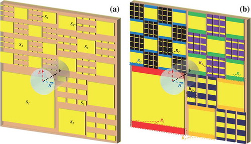
The unit cell of MMA without conductive fibers is presented in ). The proposed unit cell consists of three layers: patterned-copper, FR4-dielectric and continuous copper layers. The dielectric layer is located between patterned copper patterns at the front and copper plane at the bottom. The unit cell contains rectangular copper patches, which are most suitable for our frequency band of interest and for the integration with conductive fibers, with different sizes, and the optimized unit cell reveals periodic dimensions of p = 400 mm in the x-y plane. The top patterned copper and the bottom copper plane have electric conductivity of S/m and thickness of
= 0.035 mm. The employed dielectric FR4 has dielectric constant and loss tangent of
and
, respectively, and its thickness is
= 0.8 mm. The length and the width of rectangular patch (
) are
and
. When conductive fibers are connected to the metallic rectangular patches,
and
of the largest rectangular patch were varied to determine the starting point of absorption band, resulting in high absorption at that frequency. After determining the absorption band, the number of rectangular patches was selected. In order to maintain the high performance in broadband, the absorption at the corresponding frequencies was optimized by changing
and
of the other six rectangular patches in the order of the size of rectangle. The optimized values for the length of the rectangular patch become
,
,
,
,
,
and
mm, and the corresponding widths come to be
,
,
,
,
,
and
mm. The largest rectangular patch (
) is designed to exhibit the resonance at 0.95 GHz, and the other optimized patches are devised to have periods of 1/2 (
), 1/3 (
), 1/4 (
), 1/6 (
), 1/9 (
) and 1/12 (
) of the largest rectangular patch. ) shows the unit cell of the MMA with conductive fibers. The electric conductivity of conductive fiber (
) connected with the rectangular patches (
) above and below is designated as
. The optimized values for the electric conductivity of conductive fiber come to be
,
,
,
,
and
S/m. The thickness of conductive fiber is
mm.
Figure 1. Design of the unit cell for ultrathin MMA. Three-dimensional periodic structure of the unit cell (a) without and (b) with conductive fibers.
The minimum size of fabricated MMA is mm
because of the large periodicity in the x-y plane and the low operating frequency. The patterned-copper layer was delicately etched by using a conventional photolithography process. We selected polypyrrole as the material of conductive fibers because its electrical conductivity can be controlled by doping. The electrical conductivity of fibers was measured with a four-point probe. The fibers were cut slightly longer than the marked parts (
) between the metallic rectangular patches. They were taped to connect with the copper rectangular patches as shown in .
3. Results and discussion
In order to compare the MMAs without and with the conductive fibers, we present both calculated real and imaginary parts of the relative impedance, as shown in ). As mentioned above, it is a well-known method to explain the perfect-absorption properties using the free-space impedance-matching theory [Citation25]. By using the reflection and the transmission scattering parameters, the effective impedance can be calculated as [Citation26]
Figure 2. Difference between MMA without and with conductive fibers. (a) Effective impedance and (b) simulated absorption spectrum of the proposed MMA without and with conductive fibers.
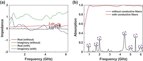
It can be observed that the real part of effective impedance of the MMA without the conductive fibers is much smaller than 1 at 0.95, 1.36, 1.70, 2.00 and 4.40 GHz except the wild fluctuation, but weak peaks appear. The imaginary part of effective impedance also presents the weak peaks at the frequencies where the weak ones are observed in the real part of effective impedance. However, the real part of effective impedance for the MMA with conductive fibers is larger than that for the MMA without conductive fibers, and the difference in the real part of effective impedance between the MMA with conductive fibers and the free space [] at 0.66–6.09 GHz is less than 0.4. When the real part of effective impedance is similar to the free space, the reflection of entire MMA structure is minimized for the incident EM wave. The imaginary part of effective impedance become 0 at 2.28, 3.26, 4.2, 4.4 and 5.28 GHz. The real parts of effective impedance at 2.28, 3.26, 4.2, 4.4 and 5.28 GHz, which are all the magnetic resonance frequencies indicated by the imaginary parts above, are 1.22, 0.76, 1.08, 0.89, and 1.37, which mean the impedance matching at these frequencies of the magnetic resonance. The difference in the imaginary part of effective impedance between the MMA with conductive fibers and the free space [
] in the region below 0.91 GHz or above 6.03 is more than 0.4. ) presents that the improved absorption by connecting the conductive fibers. The simulated absorption spectra of the MMAs without and with conductive fibers are illustrated in a frequency range of 0.50–6.20 GHz. The MMA without conductive fibers has absorption peaks at 0.95, 1.70, 2.00, 4.40 and 5.49 GHz with absorption of 15.5%, 18.0%, 30.5%, 40.0% and 35.6%, respectively. In addition, negligible weak absorption peaks also exist. On the other hand, the absorption of MMA with conductive fibers is over 97% at 0.97–6.12 GHz. In the generic equivalent RLC circuit, Q-factor associated with the loss of metallic part can be expressed by [Citation27]
In equation (2), the angular resonance frequency, the effective inductance and the effective resistance of circuit are denoted by , L and R. The operating bandwidth can be approximately determined as
Here, is the resonance frequency [
]. By connecting with the conductive fibers, the absorption band is widened by manipulating the resistance component. As the Ohmic loss responsible for the resistive part increases, the absorption also increases.
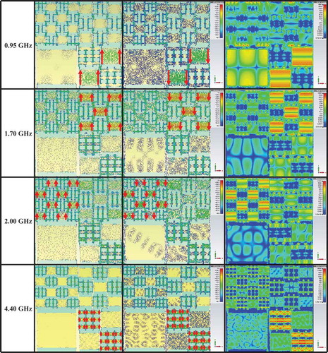
To further understand the mechanism of energy dissipation, we simulate the surface current and the power-loss density of MMA with conductive fibers at 0.95 1.70, 2.00 and 4.40 GHz, as shown in . The selected frequencies are for the absorption peaks of MMA without conductive fibers, marked by purple dashed circles in ), since the resonance frequencies are unchanged significantly even when the conductive fibers are connected. At all the frequencies, the induced surface currents in the patterned layers (the first column) are accumulated in the upward direction (indicated by red arrows) by excitation along the E field, and those in the continuous-copper plane layers (the second column) behave in the downward direction. The induced antiparallel surface currents induce a strong magnetic field in the opposite direction of the magnetic field of incident EM wave by Ampere’s law, which dissipates the incident EM wave [Citation28]. The evidence for the magnetic resonance can be demonstrated with the antiparallel surface currents between patterned- and continuous-copper layers, and it is also noticed that the induced surface currents affect the effective permittivity. In short, the high absorption occurs according to the impedance matching by the magnetic resonances. The power-loss density (dielectric loss) in the third column of provides a simple route to identify the areas that strongly absorb the EM wave at specific frequencies. At 0.95 GHz, the absorption is caused by the second-largest rectangular patches (), and it can be observed that the third-largest rectangular patches (
) also contribute greatly to the absorption. The absorption peaks at 2.00 and 4.40 GHz are affected by the fourth-largest rectangular patches (
) and the fifth-largest rectangular patches (
), respectively.
Figure 3. Physical mechanism of the broadband absorption. Simulated the induced surface currents in the metallic pattern (first column), the continuous metallic plane (second column) and three-dimensional distributions for the power loss (third column) at 0.95, 1.70, 2.00 and 4.40 GHz.
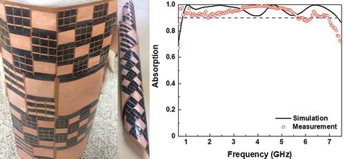
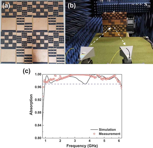
show the photographs of fabricated sample and experimental configuration, set in a microwave anechoic chamber, respectively. The fabricated MMA of copper rectangular patches with different size and with conductive fibers connected by taping is thin enough to bend. To prevent the interference effect between incident and reflected waves at an incident angle of 5°, we set the two antennas at an appropriate distance. A copper plate of the same size was used to gain the reference perfect-reflection spectrum, and the reflection spectrum () was measured differently from the simulation because there was no transmission, as shown in ). The simulated (black curve) and the measured (red dots) are plotted in ). It can observed that the experimental result display that the absorption band over 97% is slightly widened from 0.97–6.12 GHz to 0.87–6.11 GHz in comparison with the simulated one, and the overall absorption is maintained in all the measured frequency range. The experimental absorption band is red-shifted, but the experimental absorption is higher more or less than the simulation, because the electric conductivity of conductive fibers and the real properties of FR4 are slightly different from the simulation. The ratio of total thickness
of the MMA to the wavelength
at 0.97 GHz comes to be
.
Figure 4. Experiment and performance of the MMA. Photos of (a) the fabricated sample with conductive fibers and (b) the measurement set-up. (c) Simulated and measured absorption spectra for the proposed structure.
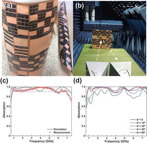
In order to take advantage of the flexible property of conductive fibers, the simulation and the experiment are implemented by substituting polyimide for FR4 and changing the thickness of copper for the same conditions. The employed flexible dielectric polyimide has the dielectric constant and the loss tangent of and
, respectively, and its thickness is
= 0.025 mm. The top patterned copper and the bottom copper plane were prepared with the thickness of
mm. present the photographs of rolled flexible sample, emphasizing the flexibility, and experimental configuration, respectively. The simulated (black curve) and the measured (red dot) are illustrated in ). In the simulation, the absorption spectrum shows that the absorption is over 90% at 0.87–7.34 GHz, and the absorption is slightly lower compared with the FR4 substrate, but the absorption bandwidth is expanded toward higher frequency. The corresponding experimental results indicate that the absorption band over 90% is divided into ranges of 0.75–5.67 and 6.23–6.97 GHz, and, in common with the case of FR4 substrate, the case of absorption band is red-shifted. In the case of the operating frequency of 0.97 GHz, the ratio of total thickness
of MMA to wavelength
is realized to be as small as
. It is possible to obtain the flexible high-absorption performance in the desired frequency range by adjusting the appropriate parameters of unit cell. To verify that the absorption of flexible MMA is maintained with respect to the incident angle, ) exhibits the absorption spectra at incident angles of 0, 15°, 30°, 45° and 60° at 0.7–7.5 GHz. As the angle of incidence increases up to 30°, the valleys become deeper, but the overall absorption over 90% is maintained in the broadband. However, the absorption is slightly lower at the absorption peaks and the valleys come to be even deeper at incident angles of 45° and 60°. These results mean that the absorption properties can be maintained even when this MMA is bent. Therefore, it can be used not only to protect electronic devices from the electromagnetic interference, but also to conceal civil and military devices from radar.
Figure 5. Application of the MMA model for flexibility. Photographs of (a) the fabricated flexible sample with conductive fibers and (b) the measurement configuration. (c) Simulated and experimental absorption spectra of the suggested flexible MMA. (d) Simulated absorption spectra according to the incident angle for the TE polarization.
4. Conclusions
The proposed structure of ultrathin and wide-band MMAs, whose meta-surface has metallic rectangular patches with different sizes and the conductive fibers for connecting metallic patches in the E-field direction, were studied by simulation and experiment for the microwave range. By exploiting the magnetic resonances and the conductive fibers in the microwave regime, the thickness of MMA was minimized to be at 0.97 GHz. The absorption spectrum was measured at 0.8–6.2 GHz and compared with the simulated one. The experimental and the simulated absorption spectra are quite similar. In addition, the absorption mechanism was understood, based on the magnetic resonance and the impedance matching. We also investigated the flexible MMA, whose dielectric was polyimide. The absorption band was widened and the high-absorption performance was maintained. The thickness of MMA was
at 0.75 GHz. Hence, we expect that our proposed ultrathin and wide-band MMAs can be applied to the flexible microwave/electronic devices, for example, microwave appliance and stealth aircraft, in the near future.
Disclosure statement
No potential conflict of interest was reported by the authors.
Additional information
Funding
References
- Shalaev VM. Optical negative-index metamaterials. Nat Photon. 2007;1:41–48.
- Wang BN , Zhou JF , Koschny T , et al. Chiral metamaterials: simulations and experiments. J Opt A: Pure Appl Opt. 2009;11:114003.
- Navarro-Cia M , Beruete M , Campillo I , et al. Enhanced lens by and near-zero metamaterial boosted by extraordinary optical transmission. Phys Rev B. 2011;83:115112.
- Hwang JS , Kim YJ , Yoo YJ , et al. Switching and extension of transmission response, based on bending metamaterials. Sci Rep. 2017;7:3559.
- Koschny T , Kafesaki M , Economou EN , et al. Effective medium theory of left-handed materials. Phys Rev Lett. 2004;93:107402.
- Shin D , Urzhumov Y , Jung Y , et al. Broadband electromagnetic cloaking with smart metamaterials. Nat Commun. 2012;3:1213.
- Yoo YJ , Yi C , Hwang JS , et al. Experimental realization of tunable metamaterial hyper-transmitter. Sci Rep. 2016;6:33416.
- Landy NI , Sajuyigbe S , Mock JJ , et al. Perfect metamaterial absorber. Phys Rev Lett. 2008;100:207402.
- Wang Y , Sun T , Paudel T , et al. Metamaterial-plasmonic absorber structure for high efficiency amorphous silicon solar cells. Nano Lett. 2012;12:440–445.
- Liu N , Mesch M , Weiss T , et al. Infrared perfect absorber and its application as plasmonic sensor. Nano Lett. 2010;10:2342–2348.
- Maier T , Bruckl H. Wavelength-tunable microbolometers with metamaterial absorbers. Opt Lett. 2009;34:3012–3014.
- Song S , Chen Q , Jin L , et al. Great light absorption enhancement in a graphene photodetector integrated with a metamaterial perfect absorber. Nanoscale. 2013;5:9615–9619.
- Khuyen BX , Tung BS , Yoo YJ , et al. Miniaturization for ultrathin metamaterial perfect absorber in the VHF band. Sci Rep. 2017;7:45151.
- Ghamsari BG , Abrahams J , Remillard S , et al. High-temperature superconducting multi-band radio-frequency metamaterial atoms. Appl Phys Lett. 2013;102:013503.
- Yoo YJ , Zheng HY , Kim YJ , et al. Flexible and elastic metamaterial absorber for low frequency, based on small-size unit cell. Appl Phys Lett. 2014;105:041902.
- Beeharry T , Yahiaoui R , Selemani K , et al. A dual layer broadband radar absorber to minimize electromagnetic interference in radomes. Sci Rep. 2018;8:382.
- Burgos SP , Waele RD , Polman A , et al. Symmetry breaking and optical negative index of closed nanorings. Nat Mater. 2010;9:407–412.
- Ma Y , Chen Q , Grant J , et al. A terahertz polarization insensitive dual band metamaterial absorber. Opt Lett. 2010;36:945–947.
- Park JW , Tuong PV , Rhee JY , et al. Multi-band metamaterial absorber based on the arrangement of donut-type resonators. Opt Express. 2013;21:9691–9702.
- Ding F , Cui Y , Ge X , et al. Ultra-broadband microwave metamaterial absorber. Appl Phys Lett. 2012;100:103506.
- Zhang C , Cheng Q , Yang J , et al. Broadband metamaterial for optical transparency and microwave absorption. Appl Phys Lett. 2017;110:143511.
- Zhang C , Yang J , Yuan W , et al. An ultralight and thin metasurface for radar-infrared bi-stealth applications. J Phys D: Appl Phys. 2017;50:444002.
- Kim HK , Ling K , Kim K , et al. Flexible inkjet-printed metamaterial absorber for coating a cylindrical object. Opt Express. 2015;23:5898–5906.
- Kim YJ , Yoo YJ , Kim KW , et al. Dual broadband metamaterial absorber. Opt Express. 2015;23:3861–3868.
- Kim YJ , Yoo YJ , Hwang JS , et al. Ultra-broadband microwave metamaterial absorber based on resistive sheets. J Opt. 2017;19:015103.
- Smith DR , Vier DC , Koschny T , et al. Electromagnetic parameter retrieval from inhomogeneous metamaterials. Phys Rev E. 2005;71:036617.
- Bilotti F , Toscano A , Vegni L , et al. Equivalent-circuit models for the design of metamaterials based on artificial magnetic inclusions. IEEE Trans Microw Theory Tech. 2007;55:2865–2873.
- Zhou J , Economon EN , Koschny T , et al. Unifying approach to left-handed material design. Opt Lett. 2006;31:3620–3622.