
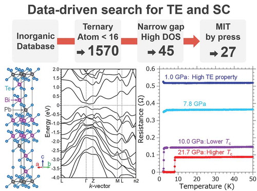
ABSTRACT
Candidate compounds for new thermoelectric and superconducting materials, which have narrow band gap and flat bands near band edges, were exhaustively searched by the high-throughput first-principles calculation from an inorganic materials database named AtomWork. We focused on PbBi2Te4 which has the similar electronic band structure and the same crystal structure with those of a pressure-induced superconductor SnBi2Se4 explored by the same data-driven approach. The PbBi2Te4 was successfully synthesized as single crystals using a melt and slow cooling method. The core level X-ray photoelectron spectroscopy analysis revealed Pb2+, Bi3+ and Te2- valence states in PbBi2Te4. The thermoelectric properties of the PbBi2Te4 sample were measured at ambient pressure and the electrical resistance was also evaluated under high pressure using a diamond anvil cell with boron-doped diamond electrodes. The resistance decreased with increasing of the pressure, and pressure-induced superconducting transitions were discovered at 2.5 K under 10 GPa. The maximum superconducting transition temperature increased up to 8.4 K at 21.7 GPa. The data-driven approach shows promising power to accelerate the discovery of new thermoelectric and superconducting materials.
GRAPHICAL ABSTRACT
1. Introduction
A data-driven approach based on high-throughput computation has recently been applied successfully to exploration of new functional materials such as battery materials, thermoelectric materials, superconductors, and so on. Once proper target quantities are selected, this approach may be more efficient than or at least complementary to traditional carpet-bombing type experiments based on experiences and inspirations of researchers [Citation1–Citation5]. We have reported a case study of the data-driven approach thorough a discovery of pressure-induced superconductivity in a compound SnBi2Se4 selected by the high-throughput screening [Citation6]. In this particular screening, the candidate compounds were explored according to a guideline that is characterized by specific band structures of ‘flat band’ near the Fermi level, such as multivalley [Citation7], pudding mold [Citation8], and topological-type [Citation9] structures. If such kinds of flat band are realized near the Fermi level, thermoelectric properties with high electrical conductivity and Seebeck coefficient would be enhanced [Citation8,Citation10]. If the flat band crosses the Fermi level, superconductivity would be realized due to high density of states (DOS) [Citation11–Citation13]. Experimentally, a single crystal of SnBi2Se4 exhibited an insulator-to-metal transition under 11 GPa [Citation6], in a good agreement with the theoretical prediction. Moreover, a pressure-induced superconductivity was observed with maximum superconducting transition temperature (Tc) of 5.4 K under 63 GPa in accordance with our scenario. That work serves as a case study of the important first step for next-generation data-driven material science.
In the aforementioned data-driven approach, a high thermoelectric performance in SnBi2Se4 is expected under high pressure around its insulator to metal transition, since the band gap decreases by the applied pressure, and then the flat band approaches the Fermi level. If a certain compound with the same crystal structure and similar band shape has narrower band gap than that of SnBi2Se4, it will show superior thermoelectric property even at ambient pressure. Furthermore, it could be expected that superconductivity may appear at much lower pressure, compared with SnBi2Se4.
Based on these considerations, we focused on PbBi2Te4 as a target compound because it has same crystal structure and similar band structure with the band gap narrower than ~200 meV of SnBi2Se4. Superior thermoelectric properties at ambient pressure and the superconductivity under lower pressure could be expected in PbBi2Te4, compared with SnBi2Se4. In this study, we successfully synthesized the sample of PbBi2Te4 in a single crystal. The crystal structure, compositional ratio, and valence states of the PbBi2Te4 single crystal were analyzed by the powder X-ray diffraction (XRD), an energy dispersive X-ray spectrometry (EDX) and an X-ray photoelectron spectroscopy (XPS), respectively. The thermoelectric properties were measured at ambient pressure. The resistivity of the obtained sample was evaluated under high pressure using a diamond anvil cell (DAC) with boron-doped diamond electrodes [Citation14-Citation17].
2. Screening procedures in high-throughput first-principles calculations
One thousand five hundred seventy candidates were listed from the inorganic material database named AtomWork [Citation18], based on the following restriction: abundant and nontoxic or less toxic constituent elements, and the number of atoms being less than 16 per primitive unit cell. The candidates were narrowed down by using the restriction of a narrow band gap and high DOS near the Fermi level. By this screening, the number of candidate compounds was reduced to 45. Finally, we checked whether the band gap decreases (or even the metallic behavior appears) under pressure of 10 GPa, and screened out 27 promising compounds. Through the above screening procedures, PbBi2Te4 was chosen as a candidate for new thermoelectric and superconducting materials. The details of our screening scheme in the high-throughput first-principles calculations were given in our previous paper [Citation6].
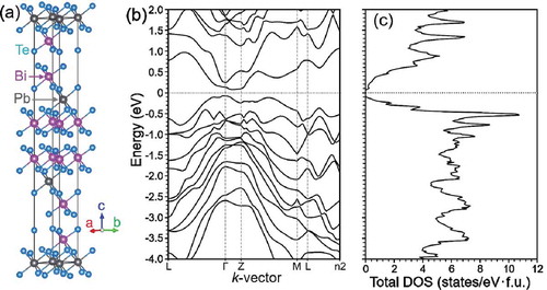
shows (a) the crystal structure of PbBi2Te4 with trigonal R-3m structure depicted by VESTA [Citation19], (b) the band structure and (c) the total DOS of PbBi2Te4 obtained by the generalized gradient approximation with spin-orbit coupling. We can see that the band edges of PbBi2Te4 show flat shape near the Fermi level. This feature is quite similar with that of SnBi2Se4. Additionally, the band gap of 101 meV in PbBi2Te4 is less than half of 208 meV in SnBi2Se4. The feature in the band structure of PbBi2Te4 at ambient pressure is similar to that of SnBi2Se4 under pressure of 5–10 GPa [Citation6]. We could expect superior thermoelectric and superconducting properties under relatively low pressure for PbBi2Te4.
Figure 1. (a) Crystal structure, (b) band structure and (c) total density of states (DOS) of PbBi2Te4 obtained by the generalized gradient approximation with spin-orbit coupling.
3. Experimental procedures
3.1. Sample synthesis
Single crystals of PbBi2Te4 were grown by a melt and slow-cooling method. Starting materials of Pb grains, Bi grains, and Te chips were put into an evacuated quartz tube in the stoichiometric composition of PbBi2Te4. The ampoule was heated at 1000 °C for 1 h, and then slowly cooled down to 800 °C within 20 h in the furnace. After keeping the temperature for 5 h, the ampoule was cooled down to room temperature. The obtained samples were ground and loaded into an evacuated quartz tube again. The sample was heated at 500 °C for 50 h for homogenization of PbBi2Te4 phase.
3.2. Characterization
The crystal structure of the obtained PbBi2Te4 samples was investigated by the powder XRD using the Mini Flex 600 setup (Rigaku) and Cu Kα radiation. The lattice constants were refined using the Conograph software (High Energy Accelerator Research Organization, Japan) [Citation20]. The chemical composition of the sample was evaluated by an EDX analysis using the JSM-6010LA microscope (JEOL). The valence state was estimated by the core level XPS analysis using AXIS-ULTRA DLD (Shimadzu/Kratos) with monochromatic Al Kα X-ray radiation (hν = 1486.6 eV), operating under a pressure of the order of 10−9 Torr. The samples were cleaved using Scotch tape in a vacuum of approximately 10−7 Torr. The analyzed area was approximately 1 × 1 mm2. The binding energy scale was established by referencing the C 1s value of adventitious carbon. The background signals were subtracted by using the active Shirley method implemented in COMPRO software (Surface Analysis Society of Japan, Japan) [Citation21]. The photoelectron peaks were analyzed by the pseudo-Voigt functions peak fitting.
3.3. Transport measurements
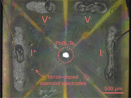
Thermoelectric properties, including the electrical resistivity, Seebeck coefficient, and thermal conductivity, were measured by using the thermal transport option (TTO) of physical property measurement system (PPMS/Quantum Design) under ambient pressure from 300 K to 2 K. The power factor and figure of merit were evaluated from the obtained parameters. Resistance measurements of PbBi2Te4 single crystal under high pressure were performed using an originally designed DAC with boron-doped diamond electrodes [Citation14–Citation17]. shows an optical image of the sample space of our DAC. The sample was placed at the center of the bottom anvil where the boron-doped diamond electrodes were fabricated. The undoped diamond insulating layer covers the surface of the bottom anvil except for the sample space and electrical terminal. The details of the cell configuration were described in the literature [Citation16]. Cubic boron nitride powder with ruby manometer was used as a pressure-transmitting medium. The applied pressure values were estimated by the fluorescence from ruby [Citation22] and the Raman spectrum from the culet of top diamond anvil [Citation23] by an inVia Raman Microscope (RENISHAW).
Figure 2. Optical image of the sample space of DAC with boron-doped diamond electrodes.
4. Results and discussion
4.1. Crystal structure, composition and valence state
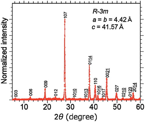
shows a powder XRD pattern of the pulverized PbBi2Te4 single crystal. All observed peaks were well indexed to trigonal R-3m structure with lattice constants of a = b = 4.42 Å and c = 41.57 Å, without any impurity peaks. Here we note that if the sample is synthesized without the annealing process at 500 °C for 50 h which is described in the experimental section, the PbBi4Te7 contamination appears. EDX analysis of the obtained single crystal yields the composition Pb0.9Bi2Te3.8 as normalized by Bi, indicating Pb deficiency in the sample. The deficient nature is consistent with a related compound SnBi2Se4 [Citation24].
Figure 3. Powder XRD pattern of pulverized PbBi2Te4 single crystal.
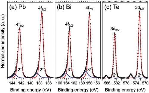
The valence states of Pb, Bi and Te in PbBi2Te4 were investigated by XPS. ) shows a Pb 4f core-level spectrum of PbBi2Te4. There are two main peaks at 142.4 eV and 137.5 eV corresponding to Pb 4f5/2 and 4f7/2 with the valence state of Pb2+ [Citation25]. ) shows a Bi 4f core-level spectrum. The Bi 4f photoemission is split into two peaks, one at around 157.8 eV attributed to Bi 4f7/2 and the other at around 163.1 eV attributed to Bi 4f5/2 [Citation26]. These main peak positions are corresponding to that of Bi3+ valence state. The Te 3d region had two groups of peaks as shown in ), which were observed at 582.8 eV and 572.4 eV, indicating the existence of Te2-, 586.5 eV and 576.1 eV of Te4+ due to a surface oxide layer [Citation27]. These Pb2+, Bi3+ and Te2- are consistent with the formal charge valence of PbBi2Te4. The Pb 4f and Bi 4f spectra contain small peaks at the higher binding energy region which may be due to the surface oxidization or the asymmetric feature of the main peaks [Citation28]. If the asymmetry can be fitted with a Doniach-Sunjic line shape [Citation29], it means the sample is metallic and has high DOS near the Fermi level [Citation30]. Figure S1 in the supplemental materials shows the outcome of peak fitting using the Doniach-Sunjic line shaped pseudo-Voigt functions. The asymmetric parameter α was 0.12 and 0.09 in Bi 4f and Pb 4f, respectively. Although the peak shape is consistent with the flat band model, further investigation is necessary to determine the reason of its asymmetry.
Figure 4. High-resolution XPS spectra of (a) Pb 4f, (b) Bi 4f, and (c) Te 3d core levels in PbBi2Te4 single crystal.
4.2. Thermoelectric properties
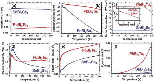
shows temperature dependence of the thermoelectric properties including (a) electrical resistivity, (b) Seebeck coefficient, (c) carrier concentration, and (d) thermal conductivity under ambient pressure for PbBi2Te4 (red curves). The results of SnBi2Se4 (blue curves) are also shown for comparison. PbBi2Te4 shows negative slope of resistivity toward lower temperature, namely metallic behavior. The absolute value of resistivity is much smaller than that of SnBi2Se4 [Citation6]. The negative Seebeck coefficient and negative slope of the Hall voltage as a function of applied magnetic field indicate n-type nature of the sample, which may be caused by the excess Bi in the crystal. If the carrier type is tuned from n-type to p-type, the thermoelectric property could be enhanced because the valence band edge provides higher DOS near the Fermi level. A high pressure application, elemental substitution, or electric double layer transistor gating are effective for such kind of band tuning. Although the absolute value of the Seebeck coefficient in PbBi2Te4 is smaller than that of SnBi2Se4, the thermal conductivity is almost same [Citation6]. Consequently, the thermoelectric properties of the power factor and figure of merit were dramatically increased in PbBi2Te4 compared to SnBi2Se4. The highest values of the power factor ~100 μWm−1 K−2 and figure of merit ~ 0.02 were obtained at 300 K. This tendency of high thermoelectric performance would be originated from the flat band with the small band gap, which is equivalent to the electronic state in SnBi2Se4 under high pressure [Citation6].
Figure 5. Temperature dependence of thermoelectric properties in PbBi2Te4 and SnBi2Se4 under ambient pressure. (a) resistivity, (b) Seebeck coefficient, (c) carrier concentration (inset is a magnetic field dependence of Hall voltage at room temperature), (d) thermal conductivity, (e) power factor, and (f) figure of merit ZT.
4.3. In situ resistivity measurement under high pressure
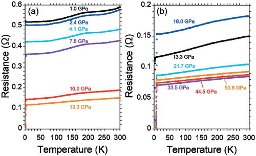
) shows a temperature dependence of resistance for PbBi2Te4 under various pressures from 1.0 GPa to 13.3 GPa. The sample has already exhibited metallic behavior under ambient pressure as shown in ). The resistance at 1.0 GPa also shows metallic behavior but with a small hump around 200 K. The resistance and the intensity of hump decreased with the increase of the applied pressure. A pressure-induced superconductivity with clear zero resistance was observed under 10 GPa. This critical pressure of the superconductivity is almost half of 20.2 GPa in SnBi2Se4. In this region, the maximum onset transition temperature (Tconset) and zero-resistance temperature (Tczero) were 3.4 K and 2.4 K under 13.3 GPa, respectively.
Figure 6. Temperature dependence of resistance in PbBi2Te4 under various pressures, (a) 1.0–13.3 GPa, (b) 13.3–50.8 GPa.
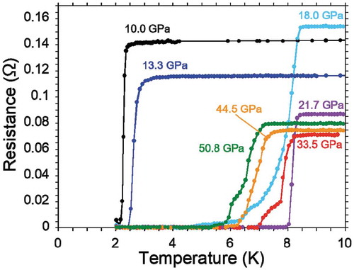
The Tc of PbBi2Te4 suddenly jumped up with the application of further pressure as same as SnBi2Se4. A temperature dependence of resistance from 13.3 GPa to 50.8 GPa is shown in ). The Tconset was enhanced from 3.4 K under 13.3 GPa to 8.1 K under 18.0 GPa. In the higher pressure region, the maximum Tconset and Tczero were 8.4 K and 7.9 K under 21.7 GPa, respectively. The temperature dependences of resistance around the superconducting transitions are summarized in . Indeed, the tendency of the Tc increases is quite similar to that of SnBi2Se4 [Citation6]. Both the critical pressures for the lower and higher Tc phases under ~10 GPa and ~20 GPa in PbBi2Te4 are almost half of ~20 GPa and ~40 GPa in the SnBi2Se4, respectively, due to the band gap difference. The higher Tc in PbBi2Te4 compared with that in SnBi2Se4 would be originated from the higher DOS near the Fermi level because the higher pressure application decreases the DOS due to an increase of bandwidth.
Figure 7. Temperature dependence of resistance around superconducting transitions in PbBi2Te4 under various pressures.
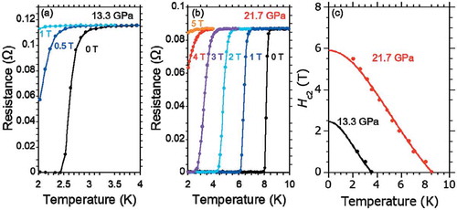
shows temperature dependence of resistance in various magnetic fields under (a) 13.3 GPa, (b) 21.7 GPa. Upper critical field Hc2//ab(0) values were estimated from the Werthamer-Helfand-Hohenberg (WHH) approximation [Citation31] for the Type II superconductor in a dirty limit. A temperature dependence of Hc2//ab values is shown in ). The Hc2//ab(0) were 2.4 T under 13.3 GPa and 5.9 T under 21.7 GPa.
Figure 8. Temperature dependence of resistance of PbBi2Te4 in specified magnetic field, under pressure of (a) 13.3 GPa or (b) 21.7 GPa. (c) Temperature dependence of Hc2//ab values at 13.3 GPa and 21.7 GPa.
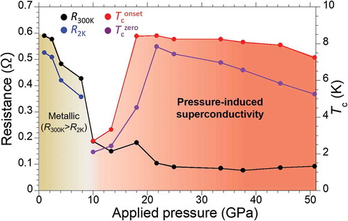
shows a resistance-pressure phase diagram of PbBi2Te4 single crystal. The resistance of the sample is dramatically decreased by applying pressure. After that, the first superconducting phase was newly discovered under 10.0 GPa. In a higher pressure region above 18.0 GPa, we observed a Tc jump from 3.4 K to 8.4 K. The Tc jump indicates a possibility of appearance of second superconducting phase. Further experimental investigation is required to clear the origin of Tc jump, for example, analysis of pressure distribution in sample space, in situ XRD measurement under high pressures, and theoretical prediction of crystal structure under high pressure. This superconductivity survived up to at least 50.8 GPa. The Tc and Hc2//ab(0) values were almost independent of the applied pressure.
Figure 9. Resistance-pressure phase diagram of PbBi2Te4.
5. Conclusion
Among 27 compounds suggested by the data-driven approach, we focused on PbBi2Te4 from the viewpoint of band similarity to the pressure-induced superconductor SnBi2Se4 which was also chosen by the data-driven approach. The PbBi2Te4 has similar flat band feature with a smaller band gap, compared to that of SnBi2Se4. The synthesized PbBi2Te4 single crystal exhibited better thermoelectric properties at ambient pressure and higher Tc value under high pressure. Especially, the superconductivity occurred under a pressure of approximately 10 GPa lower than ~ 20 GPa in SnBi2Se4, in accordance with our scenario. The present work presents a case study for the important first-step for the next generation data-driven materials science.
Supplemental Material
Download TIFF Image (120.5 KB)Acknowledgments
This work was partly supported by the “Materials research by Information Integration” Initiative (MI2I) project of the Support Program for Starting Up Innovation Hub from JST. The part of the high pressure experiments was supported by the Visiting Researcher’s Program of Geodynamics Research Center, Ehime University. The computation in this study was performed on Numerical Materials Simulator at NIMS. The authors thank Dr N. Kataoka (University of Okayama) for interpretation of XPS results.
Disclosure statement
No potential conflict of interest was reported by the authors.
Supplementary material
Supplemental data for this article can be accessed here.
Additional information
Funding
Related Research Data
References
- Ishikawa T, Oda T, Suzuki N, et al. Review on distorted face-centered cubic phase in yttrium via genetic algorithm. High Pressure Res. 2014;35:37–41.
- Ishikawa T, Nakanishi A, Shimizu K, et al. Superconducting H5S2 phase in sulfur-hydrogen system under high-pressure. Sci Rep. 2016;6:23160.
- Kiyohara S, Oda H, Miyata T, et al. Prediction of interface structures and energies via virtual screening. Sci Adv. 2016;2:e1600746.
- Seko A, Togo A, Hayashi H, et al. Prediction of low-thermal-conductivity compounds with first-principles anharmonic lattice-dynamics calculations and bayesian optimization. Phys Rev Lett. 2015;115:205901.
- Inoshita T, Jeong S, Hamada N, et al. Exploration for two-dimensional electrides via database screening and Ab initio calculation. Phys Rev X. 2014;4:031023.
- Matsumoto R, Hou Z, Hara H, et al. Two pressure-induced superconducting transitions in SnBi2Se4 explored by data-driven materials search: new approach to developing novel functional materials including thermoelectric and superconducting materials. Appl Phys Express. 2018;11:093101.
- Rowe DM. CRC handbook of thermoelectrics. Boca Raton (FL): CRC Press; 2010.
- Kuroki K, Arita R. “Pudding mold” band drives large thermopower in NaxCoO2. J Phys Soc Jpn. 2007;76:083707.
- Kopnin NB, Heikkilä TT, Volovik GE. High-temperature surface superconductivity in topological flat-band systems. Phys. Rev. B. 2011;83:220503.
- Mori K, Usui H, Sakakibara H, et al. Theoretical expectation of large Seebeck effect in PtAs2 and PtP2. J Phys Soc Jpn. 2014;83:023706.
- Fries KS, Steinberg S. Fermi-level characteristics of potential chalcogenide superconductors. Chem. Mater. 2018;30:2251–2261.
- Sano W, Koretsune T, Tadano T, et al. Effect of Van Hove singularities on high-Tc superconductivity in H3S. Phys. Rev. B. 2016;93:094525.
- Ge Y, Zhang F, Yao Y. First-principles demonstration of superconductivity at 280 K in hydrogen sulfide with low phosphorus substitution. Phys. Rev. B. 2016;93:224513.
- Matsumoto R, Sasama Y, Fujioka M, et al. Note: novel diamond anvil cell for electrical measurements using boron-doped metallic diamond electrodes. Rev Sci Instrum. 2016;87:076103.
- Matsumoto R, Irifune T, Tanaka M, et al. Diamond anvil cell using metallic diamond electrodes. Jpn J Appl Phys. 2017;56:05FC01.
- Matsumoto R, Yamashita A, Hara H, et al. Diamond anvil cells using boron-doped diamond electrodes covered with undoped diamond insulating layer. Appl Phys Express. 2018;11:053101.
- Matsumoto R, Hara H, Tanaka H, et al. Pressure-Induced Superconductivity in Sulfur-Doped SnSe Single Crystal Using Boron-Doped Diamond Electrode-Prefabricated Diamond Anvil Cell. J Phys Soc Jpn. 2018;87:124706.
- Xu Y, Yamazaki M, Villars P. Inorganic materials database for exploring the nature of material. Jpn J Appl Phys. 2011;50:11RH02.
- Momma K, Izumi F. VESTA3 for three-dimensional visualization of crystal, volumetric and morphology data. J. Appl. Crystallogr. 2011;44:1272–1276.
- Oishi-Tomiyasu R. Robust powder auto-indexing using many peaks. J Appl Cryst. 2014;47:593–598.
- Matsumoto R, Nishizawa Y, Kataoka N, et al. Reproducibility of XPS analysis for film thickness of SiO2/Si by active Shirley method. J Electron Spectrosc Relat Phenom. 2016;207:55–59.
- Piermarini GJ, Block S, Barnett JD, et al. Calibration of the pressure dependence of the R1 ruby fluorescence line to 195 kbar. J. Appl. Phys. 1975;46:2774–2780.
- Akahama Y, Kawamura H. High-pressure Raman spectroscopy of diamond anvils to 250 GPa: method for pressure determination in the multimegabar pressure range. J. Appl. Phys. 2004;96:3748–3751.
- Heinke F, Urban P, Werwein A, et al. Cornucopia of structures in the pseudobinary system (SnSe)xBi2Se3: a crystal-chemical copycat. Inorg Chem. 2018;57:4427–4440.
- Zatsepin DA, Boukhvalov DW, Gavrilov NV, et al. XPS-and-DFT analyses of the Pb 4f-Zn 3s and Pb 5d-O 2s overlapped ambiguity contributions to the final electronic structure of bulk and thin-film Pb-modulated zincite. Appl. Surf. Sci. 2017;405:129–136.
- Kong D, Cha JJ, Lai K, et al. Rapid surface oxidation as a source of surface degradation factor for Bi2Se3. ACS Nano. 2011;5:4698.
- Baghchesara MA, Yousefi R, Cheraghizade M, et al. A simple method to fabricate an NIR detector by PbTe nanowires in a large scale. Matter Res Bull. 2016;77:131–137.
- Wakita T, Paris E, Mizokawa T, et al. Determination of the local structure of CsBi4-xPbxTe6 (x = 0, 0.5) by X-ray absorption spectroscopy. Phys Chem Chem Phys. 2016;18:25136–25142.
- Doniach S, Šunjić M. Many-electron singularity in X-ray photoemission and X-ray line spectra from metals. J Phys C. 1970;3:285–291.
- Citrin PH, Wertheim GK, Baer Y. Surface-atom X-ray photoemission from clean metals: Cu, Ag, and Au. Phys. Rev. B. 1983;27:3160–3175.
- Werthamer NR, Helfand E, Hohenberg PC. Temperature and purity dependence of the superconducting critical field, Hc2. III. Electron spin and spin-orbit effects. Phys. Rev. 1966;147:295–302.