
 ?Mathematical formulae have been encoded as MathML and are displayed in this HTML version using MathJax in order to improve their display. Uncheck the box to turn MathJax off. This feature requires Javascript. Click on a formula to zoom.
ABSTRACT
The rapid advancement in intelligent bionics has elevated electronic skin to a pivotal component in bionic robots, enabling swift responses to diverse external stimuli. Combining wearable touch sensors with IoT technology lays the groundwork for achieving the versatile functionality of electronic skin. However, most current touch sensors rely on capacitive layer deformations induced by pressure, leading to changes in capacitance values. Unfortunately, sensors of this kind often face limitations in practical applications due to their uniform sensing capabilities. This study presents a novel approach by incorporating graphitic carbon nitride (GCN) into polydimethylsiloxane (PDMS) at a low concentration. Surprisingly, this blend of materials with higher dielectric constants yields composite films with lower dielectric constants, contrary to expectations. Unlike traditional capacitive sensors, our non-contact touch sensors exploit electric field interference between the object and the sensor’s edge, with enhanced effects from the low dielectric constant GCN/PDMS film. Consequently, we have fabricated touch sensor grids using an array configuration of dispensing printing techniques, facilitating fast response and ultra-low-limit contact detection with finger-to-device distances ranging from 5 to 100 mm. These sensors exhibit excellent resolution in recognizing 3D object shapes and accurately detecting positional motion. Moreover, they enable real-time monitoring of array data with signal transmission over a 4G network. In summary, our proposed approach for fabricating low dielectric constant thin films, as employed in non-contact touch sensors, opens new avenues for advancing electronic skin technology.
GRAPHICAL ABSTRACT
IMPACT STATEMENT
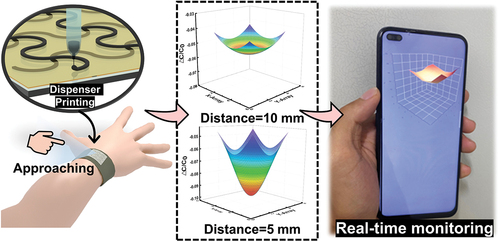
We’ve created 3D recognition sensing arrays using a printed method, enabling remote data transmission. We’ve identified an intriguing interfacial effect in GCN/PDMS doping, opening new possibilities in smart skin technology.
Introduction
Significant progress has been made in developing flexible electronics with unique properties such as reversible bending, twisting, and folding in the past few years [Citation1–5]. These advancements have resulted in a wide range of possibilities for functional versatility in wearable devices for humans. Notably, the integration of flexible haptic sensors as input and sensing components have emerged as a crucial aspect in developing electronic human skin. These sensors hold immense potential and find extensive applications in various fields, such as health monitoring [Citation6–9], human-computer interaction [Citation10–13], and bionic robotics [Citation14–16]. This widespread utilisation of flexible haptic sensors illustrates their promising prospects and wide range of applications.
Printed electronics technology [Citation17–19] offers significant advantages over traditional photolithography, particularly process efficiency and waste reduction. It proves to be advantageous for mass production. In this regard, dispense printing technology stands out due to its ability to deposit high ink concentrations and achieve flexible patterning, surpassing other printing methods like inkjet and screen printing [Citation20–22]. Moreover, it enables shorter processing time and higher precision in producing electronic products. Typically, capacitive sensors consist of two parallel electrodes with a dielectric layer in between [Citation23]. Indium, a tin oxide material commonly used as the electrode material for capacitive sensors, presents challenges in terms of preparation and lacks the required flexibility for wearable sensor applications. On the other hand, since their discovery [Citation24] in 1991, multi-walled carbon nanotubes (MWCNTS) have gained widespread use due to their exceptional mechanical and electrical properties [Citation25]. They offer a viable alternative for addressing the flexibility requirements of wearable sensor scenarios. CNTs exhibit covalent sp2 hybridisation bonds between carbon atoms, resulting in their high stiffness and resistance to axial stress. Leveraging these properties, we utilise CNTs as electrode inks in dispense printing. This enables us to meet the requirements of wearable touch sensor applications, including kinking, sliding, and compression.
Traditional methods for sensing the three-dimensional shape of objects typically entail the deformation of a capacitive layer through physical contact, posing challenges when aiming to recognize non-contact objects for electronic skin applications [Citation26]. Non-contact object sensing encompasses various techniques, including the utilization of infrared light [Citation27], magnetic induction [Citation28], and ultrasonic methods [Citation29]. Among these, capacitive sensors have emerged as particularly noteworthy due to their distinct characteristics, including high impedance necessitating minimal input energy, excellent temperature stability, and straightforward structures with unique adaptations. Li et al. [Citation30] introduced a capacitive non-contact sensor with a ‘sandwich’ configuration. This sensor employs copper electrodes, precisely fabricated through controlled in-situ laser direct patterning. The fabrication process entails the curing of a dielectric material, PDMS, positioned between two orthogonal arrays of electrode layers. This sensor boasts an effective detection distance of 200 mm and achieves a maximum sensitivity of approximately 30%. It is essential to note that non-contact capacitive sensors differ from their conventional contact-based counterparts, often influenced by the surrounding air, which possesses a low dielectric constant [Citation31,Citation32]. Consequently, a capacitive layer with a higher dielectric constant does not necessarily translate to an amplified fringing electric field, leading to diminished device sensitivity. Remarkably, the introduction of slight doping of 2D GCN [Citation33] into PDMS yields a composite film with a lower dielectric constant. This counterintuitive outcome stems from GCN’s role in restricting the mobility of PDMS molecular chains and creating numerous voids at the interface, collectively reducing overall polarization and hence the dielectric constant [Citation34].
In the context of fabricating sandwich-structured capacitive sensors, conventional device preparation techniques like photolithography and lasers offer substantial advantages over printed electronics, notably in terms of process efficiency and minimal wastage, holding potential for large-scale device production. Among these techniques, dispensing printing stands out due to its suitability for high-viscosity inks. Carbon-based electrode inks and GCN/PDMS capacitive layer inks, possessing favorable rheology and viscosity, are well-suited for dispensing printing, expediting the creation of snake arrays for touch sensors.
This study presents a capacitive touch sensor array, fully prepared via dispensing printing, with multi-walled carbon nanotube (MWCNT) ink serving as the electrode layer and GCN/PDMS ink as the capacitive layer. Intriguingly, the combination of these two high dielectric constant materials results in a decreased dielectric constant, contrary to expectations. The fabricated non-contact touch sensor device exhibits the capability for ultra-low limit object detection. Configured as a 5 × 5 array for gesture recognition and localization, the fully printed capacitive touch sensor is integrated with a printed circuit board (PCB) for wireless data transmission over 4 G networks. This integrated system facilitates remote detection of human movement and supports virtual keyboard applications.
Materials and methods
Materials
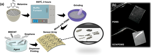
Multi-walled carbon nanotubes(MWCNT, >97%, mean diameter 3–15 nm and length 15–30 μm)and Graphene(>98%, sheet size 7–12 μm) were purchased from Shenzhen Suiheng Technology Co.; Poly(styrene sulfonic acid)(PSS, Mw = 45,000–70,000) was purchased from Macklin; Polyethylene oxide (PEO, Mw = 600,000) was purchased from Aladdin Reagent Co., Ltd., (Shanghai, China); Anhydrous ethanol(CH3CH2OH, ≥99.7%, Mw = 40.67) was purchased from Tianjin Fuyu Fine Chemical Co., Ltd. Sylgard 184 Silicone Elastomer Kit was purchased from Dow Corning Corporation. The specific flow of preparing the touch sensor is shown in .
Figure 1. (a) The preparation process of non-contact touch sensor. (b) The physical image of prepared the PDMS film and GCN/PDMS film.
Synthesis of GCN
An appropriate quantity of melamine powder was carefully measured and placed into a crucible, where it was compacted and subsequently positioned inside a heating furnace. The temperature within the furnace was then gradually raised at a rate of 20°C per minute until it reached 550°C, at which point it was maintained for a duration of 2 hours. Following this thermal treatment, the resulting GCN material was subjected to mechanical grinding using a mortar and pestle, resulting in the production of a fine, light yellow GCN powder [Citation35].
Fabrication of touch sensor
Preparation of carbon-based electrode ink
Weigh 0.11 g of multi-walled carbon nanotubes and 0.04 g of graphene, add to 6 g of deionized water and 1.5 g of anhydrous ethanol, add 0.3 g of PSS as a dispersing agent, ultrasonicate and shake for 90 minutes to obtain a uniform dispersion of carbon nanotubes and graphene. Then 0.2 g of PEO was added as a binder to improve the adhesion of the conductive ink to the PET substrate, and it was magnetically stirred at 50°C and 300 rpm for 24 hours to obtain a conductive ink with excellent performance to be dispensed for printing electrodes.
Preparation of GCN/PDMS composite film with dielectric layer ink
An appropriate amount of GCN was weighed and added to the PDMS main agent and magnetically stirred at 50°C and 300 rpm for 24 hours to uniformly disperse the GCN in the PDMS main agent. The PDMS main component was then mixed with the hardener in a ratio of 10:1 and the air bubbles were removed by vacuum after thorough stirring. The weight ratios of GCN in PDMS tested were 0, 0.25, 0.5, 0.75 and 1 wt%. The physical image of prepared the PDMS film and GCN/PDMS film is shown in .
Printing process of touch sensor
PET was used as the substrate, and the upper and lower electrodes with GCN/PDMS composite membrane formed a sandwich structure sensor. The upper and lower electrodes are selected with 27 G needles and the distance between the needles and the substrate is 0.1 mm. The printing is completed at a speed of 5.5 mm/s under a pressure of 7 kPa according to the pre-drawn pattern, while the carrier table is heated to 70°C to accelerate the solidification of the electrode part. For the intermediate dielectric layer part, a 27 G needle with a distance of 0.1 mm between the needle and the substrate was selected, and the printing was completed at a speed of 4.5 mm/sec under a pressure of 5 kPa according to a pre-drawn pattern, while the carrier table was heated to 70°C to accelerate the solidification of the laminated film, followed by UV (254 nm) surface treatment of the film.
Characterization
The electrodes and cross-sections of the sensors were characterized by optical microscopy (Nikon Eclipse LV100ND, Japan) and field emission scanning electron microscopy (Hitachi Regulus 8100, Japan), respectively. The carbon-based electrodes were analyzed by Raman spectroscopy using a Microscopical Laser Raman spectroscopy (Thermo Fisher Scientific DXR2, U.S.A.). The surface morphology of the PDMS film as well as the PDMS/GCN composite film was measured with an atomic force microscope (Bruker Dimension Icon, Germany). X-ray photoelectron spectroscopy (XPS) analysis was performed using an X-ray photoelectron spectrometer (Thermo Fisher Scientific K-Alpha, U.S.A.). FT-IR spectroscopy of the samples was carried out using a Fourier transform infrared spectrometer (Thermo Fisher Scientific IS50, U.S.A.). X-ray diffraction (XRD) measurements were completed using an X-ray diffractometer (Rigaku Ultima IV, Japan). Ultraviolet – visible spectroscopy (UV-vis) analysis was performed by Cary5000 (Cary5000, Agilent Technologies, Korea).
Capacitance measurements of the proposed capacitive sensor were obtained using a precision impedance analyzer (Wayne Kerr WK6500B, UK). The capacitance was measured at a frequency of 10 kHz and a supply voltage of 1.0 V. The change in capacitance was measured by repeatedly using a finger. It was also confirmed that the capacitance fully recovered its initial value after releasing the contact. Other conditions, including temperature and humidity, were strictly controlled to obtain accurate measurements.
Results and discussion
Characteristics of printed touch sensor
The electrodes in the flexible capacitive sensor play a crucial role in its performance. The ink components were carefully optimised to achieve an electrode ink with desirable mechanical properties, electrical properties, and printability. Various weight ratios of CNTs and graphene were tested, including 0.08 g/0.04 g, 0.11 g/0.02 g, 0.11 g/0.03 g, and 0.11 g/0.04 g. These ratios were used to prepare four sets of electrode samples with a width of 1 mm, numbered 1 to 4. Figure S1 illustrates the resistance changes of these electrode sets as the length incrementally increases from 2 mm to 10 mm. The combination of MWCNTS and the conductive network of graphene demonstrates a synergistic effect. The MWCNTS are intercalated within the layer-like structures of graphene, optimising the electron transport properties of the electrodes. Additionally, the tubular structure of MWCNTS provides entanglement, which proves advantageous for meeting the mechanical property requirements of wearable devices. After considering the mechanical properties, electrical properties, and printability of the electrodes, ink with a weight ratio of 0.11 g/0.04 g of MWCNTS to graphene was identified as the optimal formulation for the electrode preparation.
illustrates the process flow diagram for fabricating a fully printed touch sensor using a dispensing machine. The sensor structure follows a typical sandwich structure, consisting of three main components: (i) polyethylene terephthalate (PET) substrate; (ii) dot-printed carbon-based electrode array with a conductivity of 317.1 ohm/square foot; and (iii) insulating layer comprising a 120 μm thick GCN/PDMS film. demonstrates through optical microscopy that the dispensed printed carbon-based electrode exhibits a uniform curve profile even at 20× magnification. It adheres evenly to the surfaces of the GCN/PDMS film. Additionally, depicts the GCN/PDMS film at 20× magnification, showing no significant agglomeration of large particles. This indicates that the GCN particles are uniformly blended with the film, forming a high-quality composite film.
Figure 2. Flexible capacitive touch sensor. (a) Schematic diagram of the printing process of the sensor. (b) OM image of the carbon electrode printed by dispensing. (c) OM image of GCN/PDMS (0.75 wt%) dielectric layer. (d) The physical image of the sensor. (e) The cross-sectional electron microscope image of a sensing unit of the sensor. (f) Water contact angle of dielectric layer before and after UV treatment. FEM strain distribution analysis of the strain distribution along the (g) X-axis and (h) Y-axis. (i) Relative resistance changes under different tensile strains. (j) Resistance of electrodes of length 10 mm at 100 locations. (k) GCN/PDMS with different doping weight ratios at 10 kHz frequency capacitance of the composite film. (l) Relationship between GCN concentration and device capacitance value.
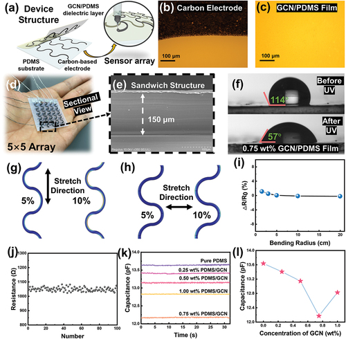
presents a 5 × 5 touch sensor array comprising 25 channels, with a size of 4 × 4 cm. The patterned carbon-based electrodes have a width of 1 mm, and there is an 8 mm spacing between the electrodes. The electrode design takes the form of a snake shape, allowing for the conversion of applied tensile strain into the local bending motion of the electrodes. This design ensures stable device performance, particularly in wearable applications. displays a cross-sectional scanning electron microscopy (SEM) image of the touch sensor structure. It exhibits the sandwich structure, with the capacitive layer having a thickness of approximately 120 μm. The upper and lower electrodes are uniformly attached to the surface of the GCN/PDMS film, fitting closely to the PET substrate. This close attachment ensures the proper functioning of the sensor. Since the electrode ink used in this study utilises a pro-biological water base as the solvent, the surface tension of the water-based ink is often too high to achieve high-precision patterning. Therefore, a high hydrophilic property is required for the printed adhesion layer. UV treatment is employed on the GCN/PDMS film surface to address this. As illustrated in , the contact angle undergoes a transition from 114° to 57° following UV treatment. This alteration is attributed to the conversion of a portion of the -OSi(CH3)2O- groups on the PDMS surface into -O4Si(OH)4-n groups. The FTIR spectra of the PDMS membranes, both before and after UV treatment, are presented in Figure S2. The characteristic peaks at 780, 1020, and 1250 cm−1 in the FTIR spectra are indicative of PDMS. Specifically, the bands at 780 cm−1 and 1250 cm−1 correspond to the Si-C wobble vibration and -CH3 deformation in the Si(CH3)2 moiety, respectively. UV treatment significantly reduces the intensity of the absorption bands at 780 and 1250 cm−1 due to the oxidation of PDMS. Additionally, the broad intensity band at 1020 cm−1, representing asymmetric Si-O-Si stretching vibrations, undergoes notable changes in shape and frequency under UV-ozone exposure. This suggests a transformation from Si coordinated with two oxygen atoms in PDMS to Si coordinated with four oxygen atoms, resulting in the formation of SiOx films through PDMS oxidation. The process involves the decomposition of -OSi(CH3)2O- groups on the PDMS surface through cleavage and redox reactions, ultimately forming polar hydrophilic groups such as OH, COOH, CO, and COO on the material’s surface. These surface functional groups facilitate better contact between water molecules and the PDMS surface, forming a uniform electrode layer [Citation36]. Figure S3 provides additional information on the water contact angles of GCN/PDMS composite membranes with different weight ratios before and after UV treatment. This data helps to assess the hydrophilic properties of the membranes.
The snake-shaped electrodes in the touch sensor design exhibit resistance to tensile loading in the parallel direction and have a margin of tensile strength for loading in the perpendicular direction to the electrode alignment. This unique feature enhances the attachment of the flexible touch sensor to complex skin surfaces and ensures device stability, particularly at joints. To evaluate the strain distribution under different tensile strains applied in various directions and at different strengths, finite element analysis (FEA) was conducted using a representative volume cell model (Figure S4). display the simulated structures, illustrating that tensile loads of up to 10% along the X and Y directions in the serpentine electrode array do not lead to device failure. This analysis confirms the robustness and reliability of the touch sensor design under different tensile loading conditions. Adding mechanical strain to a touch sensor can broaden its applications as a wearable electronic device. The serpentine electrode structure in the touch sensor design plays a crucial role. When subjected to tensile stress, the serpentine electrode straightens out, effectively preventing electrode fracture and ensuring the sensor’s integrity. This mechanism enhances the stability of the touch sensor when attached to different parts of the human body, such as the palm, where it may experience varying levels of strain. The inherent hydrophobic nature of the PDMS substrate presents a common challenge in the precise printing of uniform snake-shaped electrodes on its surface without inducing alterations in surface roughness. Furthermore, due to the interfacial properties of loosely adhered electrodes on PDMS, their utilization in flexible electronic devices for wearable applications often results in electrode detachment, consequently leading to device malfunction. As depicted in , we observed the variation in sensor electrode line resistance under different bending radii. In this experiment, the bending radius of the touch sensor was systematically reduced from 20 mm to 1.5 mm, and it is noteworthy that the change in electrode resistance remained within a margin of less than 2% throughout this bending process. This observation underscores the exceptional stability and resilience of the touch sensor against bending stress. Furthermore, upon returning the sensor to its original unbent state, it exhibited complete recovery, a behavior in alignment with our simulation results. Figure S5 provides further insights into the behaviour of the touch sensor by showing the variation in relative capacitance and resistance at different bending radii.
The uniformity and reproducibility of electrode resistance are crucial for ensuring the reliability of sensor applications. Multiple electrodes were manufactured using the dispensing printing technique, and resistance measurements were conducted at various locations with an electrode length of 10 mm, as depicted in . The results from 100 electrode samples demonstrated excellent uniformity and reproducibility, with resistance values centered around 1050 ohms. Additionally, we assessed the resistance of electrodes with varying lengths at different positions, as illustrated in Figure S6. The measurement outcomes affirm the robust stability of electrode resistance across different lengths, underscoring its significance in guaranteeing the reliability of the sensor.
To analyse the effect of doping weight ratios on the capacitance performance of GCN/PDMS composite films, various compositions ranging from 0 wt% to 0.75 wt% of GCN were examined at high frequencies (10 kHz). The results indicate that as the mass ratio of GCN increases, the capacitance of the composite films decreases. However, when the GCN mass ratio is further increased to 1 wt%, the capacitance exhibits an increasing trend (). Notably, the dielectric constants of GCN and PDMS are approximately 4.6 and 2.8, respectively, at room temperature. These values contribute to the overall capacitance behaviour observed in the GCN/PDMS composite films.
display the AFM images of pure PDMS with GCN/PDMS nanocomposites (30 × 30 μm). Small bumps of approximately 300 nm in size are observed in the nanocomposites containing GCN, indicating a slight increase in surface roughness compared to pure PDMS (RMS = 34.6 μm). However, there is no significant agglomeration of larger particles, and the dispersion of GCN with larger particles in the polymer matrix is effectively achieved through the mechanical effects of the preparation process. Furthermore, the surface of the nanocomposites exhibits more elliptical and spherical bumps than the lamellar structure observed in the graphite phase of carbon nitride. These rounded bumps are pores and cavities introduced after the composite formation. This change is attributed to the bonding between GCN and PDMS polymers, which is influenced by the weak interaction between PDMS and GCN. As a result, more cavities and pores are formed within the GCN and at the GCN/PDMS interface. Simultaneously, we employed SEM to observe a substantial quantity of cavities within the composite film (Figure S7). These cavities exhibited dimensions in the range of 200–400 nm and were prominently situated at the interface between GCN and PDMS. This observation is in accordance with the findings obtained through AFM characterization, thereby reinforcing the robustness of our results. This observation supports the finding that the dielectric constant of the nanocomposites decreases as the doping concentration of GCN increases at low levels. Moreover, the slight increase in RMS roughness of the nanocomposite leads to an increased contact area between the ink and the surface during printing. This increased contact area enhances the interaction force, which is beneficial for achieving uniform printing on the film surface, especially when using a high concentration of carbon-based ink.
Figure 3. GCN/PDMS dielectric layer analysis. (a-b) AFM images of pure PDMS and 0.75 wt% GCN/PDMS surface roughness. (c-d) AFM images of pure PDMS and 0.75 wt% GCN/PDMS microstructure; (e) XPS of 0.75 wt% GCN/PDMS dielectric layer spectra. (f) XPS spectrum of GCN/PDMS in C1s region. (g) XPS spectrum of GCN/PDMS in O region; (h) XPS spectrum of GCN/PDMS in Si region. (i) Schematic diagram of the principle of dielectric constant reduction by GCN-doped PDMS. (j) GCN/PDMS at different weight ratios infrared spectra of PDMS; (k) XRD patterns of GCN/PDMS with different weight ratios. (l) Raman diagrams of MWCNT/Graphene electrodes with different ratios.
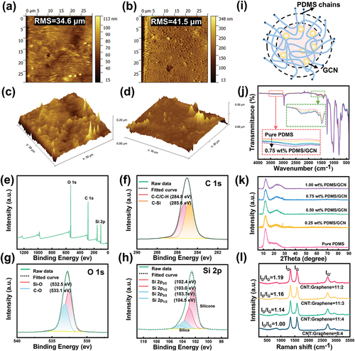
In , the XPS spectrum of the GCN/PDMS sample reveals the presence of Si, O, and C elements in the composite. The low concentration of carbon nitride doping results in a small peak of the N element, indicating that the PDMS matrix remains the predominant component in the nanocomposite films with low levels of carbon nitride doping. The C1s spectrum can be deconvoluted using symmetric Gaussian-shaped peaks for mathematical analysis. shows the fitted peaks corresponding to C-C/C-H at 284.8 and C-Si at 285.6 eV in the fine spectrum of the C element. In , the O1s peak can be deconvoluted into two peaks representing the Si-O bond at 532.5 eV and the C-O bond at 533.9 eV. The Si 2p peak in is formed by the convolution of four components: Si 2p3/2 and the two spin-orbit doublets of Si 2p1/2. Four major peaks at 102.4, 103.0, 103.7 and 104.5 eV in the Si 2p region correspond well with silicone 2p3/2, 2p1/2, silica 2p3/2, and 2p1/2, respectively. This observation indicates the presence of silica within the PDMS composite, which might have been introduced through the Sylgard 184 system. The presence of silica provides evidence for enhanced hydrophilicity following UV treatment.
The theoretical model depicted in effectively elucidates the phenomenon of diminishing dielectric constants in both GCN and PDMS materials following their composite formation. This reduction can be attributed to the relatively low doping concentration of carbon nitride, causing the composite material to approach the dielectric constant of the PDMS matrix. The incorporation of GCN via doping creates a novel interconnecting network structure within the composite, thereby constraining the mobility of PDMS molecular chains. Consequently, this restriction hinders the free movement and orientation of these molecular chains, leading to a decrease in the polymer matrix’s polarizability. Conversely, the interaction between GCN and PDMS is predominantly governed by weak van der Waals forces and hydrogen bonding, resulting in the formation of voids at the interfaces between carbon nitride and PDMS. These voids augment the free volume within the hybrid system. When subjected to an electric field, these voids exhibit limited charge storage capacity, resulting in an overall reduction in system polarization. Therefore, the presence of these voids contributes to the decline in the dielectric constant [Citation37,Citation38].
FT-IR spectroscopy characterised different weight ratios (0, 0.25, 0.5, 0.75, and 1 wt%) of GCN/PDMS, as shown in . In the 0 wt% GCN/PDMS sample, strong FT-IR peaks were observed at 789–796 cm−1 corresponding to the -CH3 swing and Si-C stretching in Si-CH3; 1020–1074 cm−1 associated with Si-O-Si stretching; 1260–1259 cm−1 representing CH3 distortion in Si-CH3; and 2950–2960 cm−1 indicating asymmetric CH3 stretching in Si-CH3. These peaks remain observable even when GCN is incorporated into PDMS at different weight percentages. The newly observed spectral band centered at 3250 cm−1 (highlighted by the red dashed rectangle) exhibits an increasing intensity with higher GCN doping concentrations. The band is associated with the N-H stretching vibrations of the terminal reactive group present in the GCN polymer. Simultaneously, the N-H stretching vibrations corresponding to 1241 and 1624 cm−1 (highlighted by the green dashed rectangle) show significant shifts in their peak positions. These shifts indicate the presence of C-N and C=N stretching vibrations, respectively (Supporting Information, Table S1). Furthermore, the characteristic respiration pattern of the triazine unit is observed at 810 cm−1, which is associated with the absorption band of the S-triazine ring. The observed spectral changes suggest the formation of hydrogen bonds within the GCN/PDMS nanocomposite. The existence of hydrogen bonding induces localized charge rearrangement, exerting an influence on the polarization effect and ultimately diminishing the overall material polarization. This decline in polarization precipitates a reduction in the dielectric constant of the nanocomposite. These findings effectively corroborate the theoretical model presented earlier. Additionally, the characteristic breathing pattern of the triazine unit at 810 cm−1 is well preserved in all GCN/PDMS samples. However, this pattern is overshadowed by the PDMS signals, such as the -CH3 wobble peak at 789 cm−1 and the Si-C stretching peak at 796 cm−1, indicated by the red dashed rectangle. The bands observed at 1624, 1553, 1409, and 1241 cm−1 are attributed to the stretching vibration modes characteristic of triazine units derived from repeating units within the GCN/PDMS nanocomposite. It is clear from these vibrational modes of the nanocomposite that triazine units have been incorporated into the structure of the nanocomposite.
XRD analysis was performed to investigate the properties of GCN/PDMS composite films with different weight ratios. The XRD patterns obtained at 500°C, 600°C, and 700°C exhibit two distinct peaks located at 2θ = 12.8° and 27.7° (Figure S8). These peaks can be attributed to the hexagonal phase of GCN. It is well-established that GCN is composed of polymerised melem building blocks. The strongest peak at 2θ = 27.7°Corresponds to the interlayer stacking of the (002) melem planes. In the GCN structure, this peak indicates a well-defined stacking arrangement. A peak at 2θ = 2.8° is also observed, which is attributed to the (100) planes. This peak is associated with the in-plane ordering of the nitrogen-linked heptazine units in the GCN structure. A clear sheet structure appeared in the SEM of GCN annealed at 600°C (Figure S9). In , the XRD pattern of pure PDMS displays a prominent peak at around 12.11°, indicating the characteristic amorphous nature of PDMS. Additionally, a broad peak is observed around 21.9°, further confirming the amorphous structure of PDMS, especially at higher concentrations. For the composite thin film sample, it is observed that the characteristic peaks at 12.11° and 21.9° increase in intensity gradually. Moreover, the peak positions shift towards higher angles (to the right) as the doping concentration of GCN increases. This shift in peak position is attributed to the presence of GCN in the composite. GCN exhibits strong characteristic peaks at 13.20° and 27.20°, assigned to the (100) and (002) diffraction planes, respectively. The XRD analysis of the composite samples revealed distinct plots for PDMS and GCN without any impurity peaks. This indicates the production of a purer GCN/PDMS composite film. The obtained results prove that GCN is uniformly embedded within these composite films, and the grafting process does not alter the inherent properties of PDMS and GCN. The consistency between the FTIR and XPS characterisation results and the XRD analysis of the GCN/PDMS composite films further confirms the accuracy and reliability of the obtained data. The Raman spectra in exhibit two prominent peaks at 1338 and 1579 cm−1, which can be assigned to the D-band and G-band, respectively, in CNT and graphene. The D-band is associated with the degree of disorder in the system, while the G-band represents carbon atoms with a complete hexagonal structure and sp2 hybridisation. The intensity ratio (ID/IG) of the D-band to the G-band is commonly used as an indicator to evaluate the degree of disorder and the presence of defects in the material. Generally, a higher ID/IG ratio indicates that the more disordered phases have larger defects in the material. The calculated ID/IG ratio in the hybrid ink of CNTs and graphene increases as the doping concentration of CNTs increases. This can be attributed to a few reasons. Firstly, a higher concentration of CNTs introduces more defects due to the curvature structure of the sidewalls. These defects increase D-band intensity, leading to a higher ID/IG ratio. Also, the interfacial interaction between CNTs and graphene can trigger charge transfer. This charge transfer process further increases the number of defects in CNTs, thus causing an increase in the ID/IG ratio. The transfer of charge between CNTs and graphene can introduce additional electrons, which alters the electronic density of states and the material’s conductive properties. The observed difference in the electrical properties of electrodes with different mixing ratios can be attributed to these changes in the ID/IG ratio. Defects and charge transfer significantly impact the conductive behavior of hybrid inks, resulting in variations in the properties of the hybrid inks. The transmittance of the pure PDMS film and the GCN/PDMS composite film were tested separately, and the transmittance of the GCN/PDMS composite film was reduced but still had good transmittance performance (Figure S10).
Performance of printed touch sensor
When a voltage is applied across the sensor electrodes, it induces the generation of an electric field in the region between these electrodes. However, it’s essential to note that a portion of the electric field’s energy disperses into the surrounding space, giving rise to what is commonly referred to as a fringe field. When an external object, such as a finger or another grounded conductor, approaches the sensor without direct contact, it perturbs the fringe field, thereby trapping a portion of the electric charge. This perturbation results in a measurable decrease in the sensor’s capacitance value. For visual clarification, please refer to , which presents a schematic representation illustrating the evolving electric field as a finger gradually approaches the sensor. In an ideal parallel-plate capacitor, the value of the device capacitance depends on the dielectric, the relative area and the distance between the electrodes, and the stripe effect is generally neglected. If the stripe field is considered, the overall capacitance consists of two parts: the classical capacitance equation (C0) and the modified equation (ΔC) for a square parallel-plate capacitor [Citation39,Citation40]:
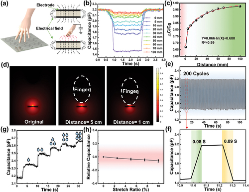
Figure 4. Electrical properties and performance of the sensor. (a) Schematic diagram of a finger approaching the sensor. (b) The relationship between the capacitance change and time of touch and proximity at a distance of 0–150 mm between the finger and the sensor. (c) The relative capacitance change between the sensor and the finger (ΔC/C0) and the distance. (d) Electric field simulation diagram at different distances between the finger and the sensor. (e) Capacitance of the sensor under 200 cycle tests; (f) response time of the sensor. (h) Capacitance of the sensor under different stretching variety. (g) Ultra-low limit detection of capacitive sensors.
Where ε0 denotes the relative dielectric constant, w and l denote the width and length of the electrodes, and d denotes the distance between the parallel plate electrodes.
The mutual capacitance (Cmc) resulting from the interaction of the fringe electric field with the target object varies with the distance between the electrodes and the target object as given in the following equation:
Where ε0 denotes the relative dielectric constant, wmc and lmc denote the width and length of the target object, and dmc denotes the distance between the electrode and the target object.
When the material’s dielectric constant (ε0) is smaller between the capacitive plates, the capacitance (C) value will decrease. In the capacitance equation, the fractional term involving the dielectric constant (ε0) is in the denominator. As ε0 decreases, the entire fractional term decreases, resulting in a decrease in capacitance. Accordingly, a capacitive layer with a smaller dielectric constant will exhibit a larger change in capacitance for a given change in the material or object being measured. High sensitivity to changes in capacitance is advantageous in certain applications where a precise measurement or detection of small changes is required.
The preceding discourse has revealed that, within the specified conditions, the capacitance of the 0.75 wt% GCN/PDMS composite film registers the lowest value. In the context of our device response tests encompassing pure PDMS, 0.25 wt%, and 0.75 wt% GCN/PDMS as dielectric layers, we now present evidence indicating that the 0.75 wt% doping concentration yields the highest response sensitivity (Figure S11). This empirical observation faithfully corroborates the earlier mentioned theoretical prediction. present the measurement results of the change in mutual capacitance for different distances between the finger and the touch sensor. These figures also depict the ratio between the capacitance change and the undisturbed value. In particular, according to Equation (2), there is a logarithmic relationship between capacitance and distance.Therefore, in , the horizontal coordinates are expressed in logarithmic terms, and the results show that when the distance is expressed in logarithmic terms, the linearity of the curve is high, with a coefficient of determination (R2) as high as 0.989.The functional relationship between capacitance and distance was then derived from the parameters of the fitted model:
The distance can be calculated in real time by measuring the capacitance change of the device for various interaction scenarios.
For the contact measurement, when the finger is in direct contact with the touch sensor surface, a change in capacitance (ΔC) of 0.72 pF was measured at a baseline capacitance of 2.19 pF. This change corresponds to a mutual capacitance change of 32.8%, indicating a high sensitivity of the touch sensor. The sensor demonstrated a strong response to the presence and touch of a finger, accurately detecting and measuring the capacitance change. During performance tests in a non-contact system, the touch sensor demonstrated the ability to perceive the distance and three-dimensional shape of approaching objects. The capacitance value measured at different distances between the finger and the sensor remained relatively stable. This stability allows for estimating distance based on the corresponding change in capacitance, enabling distance measurement functionality. For example, when the distance between the finger and the sensor is 5 mm, a capacitance change (ΔC) of 0.43 pF was observed. The distance between the finger and the sensor can be determined by analysing the change in capacitance. Similarly, even when the distance between the hand and the sensor is as large as 100 mm, a capacitance change (ΔC) of 0.064 pF was detected, indicating that the touch sensor has a detection range exceeding 100 mm and a wide response range.
The sensing unit of the sensor was carefully selected, as shown in . To analyse the effect of the sensor on the electric field at the edge of the measured object, a finite element method was employed using COMSOL software. Simulating the electric field at the edge of the capacitive sensor showed that the electric field decreases when the finger enters the electric field. As the finger enters the electric field, it disturbs the electric field. Furthermore, when the distance between the finger and the sensor is reduced from 5 cm to 1 cm, the electric field experiences a noticeable compression, reflecting the impact of proximity on the electric field distribution. In addition, the touch sensor exhibits excellent stability even after 200 cycles of testing. The initial capacitance is fully recovered after the finger is removed, indicating the sensor’s ability to maintain stable performance over multiple usage cycles (). The response and relaxation times, as depicted in , are determined to be 80 ms and 90 ms, respectively, indicating the sensor’s rapid and efficient performance. The serpentine electrode structure employed in the sensor design allows for proper functioning even under moderate stretching conditions. Based on the results obtained from previous tests and simulations, it has been determined that the sensor electrodes can withstand up to 10% tensile strain without experiencing failure. To assess the capacitance change of the sensor, measurements are conducted using a 2% increment gradient of tensile strain, as illustrated in . Under the maximum tensile strain applied along the X and Y axes, a slight decrease of approximately 5.5% in relative capacitance is observed. This reduction can be attributed to the weakening the interference effect between adjacent electrodes caused by the stretching of the sensor. However, it should be noted that the strain-induced capacitance change can potentially interfere with the sensor’s accurate touch-sensing capability. To address this issue, integrating a strain sensor with the touch sensor can be implemented, allowing error compensation and calibration of the strain’s effect on capacitance. Through this integration, accurate and reliable touch sensing can be achieved, even in the presence of strain.
In order to assess the ultra-low limit function of the proposed sensor in a contact system, a series of water drops weighing 10 mg each was carefully dispensed drop by drop using a precision micropipette. As shown in , it is evident that the touch sensor exhibits a response even when a single drop of water is present. The capacitance shows a linear increase from 2.2 pF to 2.6 pF as the number of water drops increases from 1.0 Pa (1 drop) to 5.0 Pa (5 drops), respectively. This behaviour demonstrates the high sensitivity of our proposed sensor to detect and respond to extremely low external loads.
3D recognition and IoT wearable device
Non-contact touch sensors with 3D recognition capabilities have greater potential for advancement than touch pressure sensors. They enable precise detection of objects in non-contact scenarios, making them particularly valuable for applications such as electronic skin on robots. Our proposed capacitive sensor can detect nearby objects’ positions and 3D shapes in a non-contact system. shows the measurement of finger proximity as a 3D conductive object, demonstrating the sensor’s capability in this regard. As the finger approaches the touch sensor, the mapping data clearly identifies its 3D shape. The finger’s shape becomes more distinct as the distance between the finger and the sensor decreases from 10 mm to 5 mm. Concurrently, the capacitance gradually decreases from −5.6% to −9.7% (). visually demonstrates the finger’s movement from the centre to the edge of the sensor array in the X-Y plane. These results highlight the sensor array’s (5 × 5) ability to detect and determine the shape and position of the object along all three axes. To assess the spatial resolution of the non-contact sensors, separate measurements were conducted on a circular table and a trigonal prism (). The mapped image of the round table distinctly reveals the variations in shape between the bottom and sides, allowing it to be differentiated from the mapped image of the finger. This demonstrates the sensor’s capability to recognise and distinguish different shapes. The sensing array consistently retains over 90% of its performance even after undergoing 1,000 rigorous bending fatigue tests. This resilience can be primarily attributed to the effective compensation provided by the tensile margin within the serpentine array structure, a critical factor for ensuring the applicability and durability of the array in wearable scenarios (Figure S12). Additionally, separate measurements were conducted on the trigon object, and the resulting mapped image exhibited a distinct valley-like depression shape that precisely corresponded to the actual shape of the tested object. Moreover, as a wearable device, the sensor array showcased exceptional stability throughout a wide temperature range while maintaining an impressive performance level of 98.3%, even within the temperature range of the human body’s surface. This outstanding performance signifies its significant potential for human smart skin technology applications, as shown in Figure S13.
Figure 5. 3D measurement of approaching objects. (a) Schematic diagram of 3D measurement in non-contact mode. The finger is used as the measured object. (b) 3D mapping of the relative capacitance change at two different distances (10 and 5 mm) between the finger and the sensor. The plotted surface shows the mapping result of the relative capacitance change of the 5 × 5 capacitive sensor array. (c) 3D mapping of the sensor’s relative capacitance change after changing the finger’s position. The distance is 5 mm. Detection of various shapes, such as the (d) round and (e) trigonal tables. The sensor’s centre is 5 mm away from all objects under test. (f) Block diagram and operating principle of the integrated sensing system. (g) Schematic diagram of the principle of 3D recognition sensor. (h) Real-time response signals of finger movement are measured by the sensing and displayed on a phone.
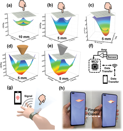
Building upon the outstanding performance of the 3D recognition sensor array, we have successfully achieved a seamless integration of the sensor array with the circuit board, resulting in a unified system capable of remotely monitoring human motion. This advanced system comprises three key modules, namely the 4 G module, the MCU (Microcontroller Unit), and the sensors. These modules establish wireless communication with various devices such as smartphones, computers, and smartwatches, leveraging the power of 4 G networks. The underlying operational principle of the system is illustrated in . The electronic skin is permanently affixed to the wrist, ensuring a continuous connection with a device dedicated to capturing and transmitting the 3D shape and displacement signals of objects using 4 G technology (). We employ a mean filtering algorithm in the data acquisition process, aimed at mitigating interference by smoothing the noise signal generated in the environment through averaging the data over a specific time range. This approach serves as a substitute for conventional shielding methods, enabling precise and highly sensitive responses. The acquired data can be seamlessly displayed in real-time on a mobile phone or any other mobile terminal, thereby facilitating remote monitoring and analysis of the test signal. As demonstrated in the Supplementary Video, the developed sensor array exhibits accurate recognition of multiple movement patterns on the mobile device. This technology holds significant potential across various application scenarios, particularly those requiring virtual keyboard input and high-precision shape recognition scanning.
Conclusions
The study successfully employed a pyrolytic synthesis method to fabricate GCN particles, which were subsequently integrated into PDMS composite films via low-concentration doping. Using a dispensing printing technique, touch sensor arrays with serpentine electrodes were developed, enabling the non-contact capacitive sensors to recognise objects’ 3D shape and positional movement. Based on the findings and discussions, the following conclusions can be drawn:
The incorporation of GCN into PDMS composite films resulted in a noticeable decrease in capacitance values, approximately 11% lower than those of pure PDMS films. This phenomenon can be attributed to two main factors. Firstly, larger GCN particles at a low concentration within the PDMS matrix hinder PDMS molecular chain mobility. This restricted mobility reduces the overall polarisation of the GCN/PDMS composite film, resulting in low capacitance values. Secondly, the interface between GCN and PDMS introduces voids or holes, which further contribute to the weakened polarisation of the composite film. These effects account for decreased capacitance values in the GCN/PDMS composite film.
The touch sensor utilised in this study employed a serpentine carbon-based electrode, which was fabricated using a dispensing printing technique to create both the upper and lower layers of the sensor. The serpentine electrode exhibited impressive characteristics, including a rapid response time of 90 ms, excellent linearity across a range of 5 mm to 100 mm, and exceptional durability withstanding 200 pull and release cycles at a large-scale strain of 10%. Moreover, the touch sensor array demonstrated remarkable stability in device performance, maintaining a level of over 98.5% even when subjected to a bending tensile strain of 10%. This outstanding stability can be attributed to the unique design of the serpentine electrode, which effectively converts applied tensile strain into a localised bending motion, ensuring consistent device performance. These features make the touch sensor suitable for various wearable applications.
The 5 × 5 touch sensor array demonstrated the ability to accurately recognise the 3D shape and positional movement of objects placed on it. This capability was evident in the XYZ axis direction. The recognition performance was attributed to the properties of the GCN/PDMS composite film, which exhibited a low dielectric constant and a high sensitivity to objects entering the electric field at the edges of the sensor.
The finger’s movement in the XY and Z axes was successfully detected, and different objects’ 3D shapes were analysed. Subsequently, the contactless touch sensor was connected to a printed, electronic circuit for signal processing and transmission. The sensor’s output signal was then displayed in real time on a personal mobile terminal using a 4 G transmission module. This achievement is an important milestone in developing electronic skin for wireless real-time monitoring. However, the capabilities of e-skin extend beyond shape and displacement detection. Therefore, future research will focus on developing more functional devices for these applications.
Author contributions
The manuscript was written through contributions of all authors. All authors have given approval to the final version of the manuscript.
Supplemental Material
Download MS Word (1.4 MB)Supplemental Material
Download MP4 Video (15.8 MB)Disclosure statement
No potential conflict of interest was reported by the author(s).
Supplementary material
Supplemental data for this article can be accessed online at https://doi.org/10.1080/14686996.2024.2311635.
Additional information
Funding
References
- Cui XH, Chen JW, Wu W, et al. Flexible and breathable all-nanofiber iontronic pressure sensors with ultraviolet shielding and antibacterial performances for wearable electronics. Nano Energy. 2022;95:107022. doi: 10.1016/j.nanoen.2022.107022
- Tay RY, Li HL, Lin JJ, et al. Lightweight, superelastic boron nitride/polydimethylsiloxane foam as air dielectric substitute for multifunctional capacitive sensor applications. Adv Funct Mater. 2020;30(10):1909604. doi: 10.1002/adfm.201909604
- He YX, Zhou MY, Mahmoud MHH, et al. Multifunctional wearable strain/pressure sensor based on conductive carbon nanotubes/silk nonwoven fabric with high durability and low detection limit. Adv Compos Hybrid Mater. 2022;5(3):1939–15. doi: 10.1007/s42114-022-00525-z
- Chen BD, Zhang L, Li HQ, et al. Skin-inspired flexible and high-performance MXene@polydimethylsiloxane piezoresistive pressure sensor for human motion detection. J Colloid Interface Sci. 2022;617:478–488. doi: 10.1016/j.jcis.2022.03.013
- Tao K, Chen ZS, Yu JH, et al. Ultra-sensitive, deformable, and transparent triboelectric tactile sensor based on micro-pyramid patterned ionic hydrogel for interactive human-machine interfaces. Adv Sci. 2022;9(10):2104168. doi: 10.1002/advs.202104168
- Gao YJ, Yu LT, Yeo JC, et al. Flexible hybrid sensors for health monitoring: materials and mechanisms to render wearability. Adv Mater. 2020;32(15):1902133. doi: 10.1002/adma.201902133
- Meng KY, Xiao X, Wei WX, et al. Wearable pressure sensors for pulse wave monitoring. Adv Mater. 2022;34(21):2109357. doi: 10.1002/adma.202109357
- Yang J, Luo S, Zhou X, et al. Flexible, tunable, and ultrasensitive capacitive pressure sensor with microconformal graphene electrodes. ACS Appl Mater Interfaces. 2019;11(16):14997–15006. doi: 10.1021/acsami.9b02049
- Xiong YX, Shen YK, Tian L, et al. A flexible, ultra-highly sensitive and stable capacitive pressure sensor with convex microarrays for motion and health monitoring. Nano Energy. 2020;70:104436. doi: 10.1016/j.nanoen.2019.104436
- Ma YA, Cheng YF, Wang J, et al. Flexible and highly-sensitive pressure sensor based on controllably oxidized MXene. InfoMat. 2022;4(9):e12328. doi: 10.1002/inf2.12328
- Wang LR, Xu TL, Zhang XJ. Multifunctional conductive hydrogel-based flexible wearable sensors. TRAC-Trends Anal Chem. 2021;134:116130. doi: 10.1016/j.trac.2020.116130
- Wei HG, Li A, Kong DS, et al. Polypyrrole/Reduced graphene aerogel film for wearable piezoresisitic sensors with high sensing performances. Adv Compos Hybrid Mater. 2021;4(1):86–95. doi: 10.1007/s42114-020-00201-0
- Chen LR, Chang XH, Wang H, et al. Stretchable and transparent multimodal electronic-skin sensors in detecting strain, temperature, and humidity. Nano Energy. 2022;96:107077. doi: 10.1016/j.nanoen.2022.107077
- Zheng YJ, Yin R, Zhao Y, et al. Conductive MXene/cotton fabric based pressure sensor with both high sensitivity and wide sensing range for human motion detection and E-skin. Chem Eng J. 2021;420:127720. doi: 10.1016/j.cej.2020.127720
- Cai YW, Zhang XN, Wang GG, et al. A flexible ultra-sensitive triboelectric tactile sensor of wrinkled PDMS/MXene composite films for E-skin. Nano Energy. 2021;81:105663. doi: 10.1016/j.nanoen.2020.105663
- Yang M, Cheng YF, Yue Y, et al. High-performance flexible pressure sensor with a self-healing function for tactile feedback. Adv Sci. 2022;9(20):2200507. doi: 10.1002/advs.202200507
- Cui Z, Han YW, Huang QJ, et al. Electrohydrodynamic printing of silver nanowires for flexible and stretchable electronics. Nanoscale. 2018;10(15):6806–6811. doi: 10.1039/C7NR09570H
- Huang QJ, Zhu Y. Printing conductive nanomaterials for flexible and stretchable electronics: a review of materials, processes, and applications. Adv Mater Technol. 2019;4(5):1800546. doi: 10.1002/admt.201800546
- Li HP, Liang JJ. Recent development of printed micro-supercapacitors: printable materials, printing technologies, and perspectives. Adv Mater. 2020;32(3):1805864. doi: 10.1002/adma.201805864
- Oliveros‐Mata ES, Voigt C, Cañón Bermúdez GS, et al. Dispenser printed Bismuth‐based Magnetic Field sensors with Non‐Saturating large magnetoresistance for touchless interactive surfaces. Adv Mater Technol. 2022;7(10):2200227. doi: 10.1002/admt.202200227
- Ogbeide O, Bae G, Yu W, et al. Inkjet‐printed rGo/binary metal oxide sensor for predictive gas sensing in a mixed environment. Adv Funct Mater. 2022;32(25):2113348. doi: 10.1002/adfm.202113348
- Ma H, Li J, Zhou J, et al. Screen-printed carbon black/recycled Sericin@ Fabrics for wearable sensors to monitor sweat loss. ACS Appl Mater Interfaces. 2022;14(9):11813–11819. doi: 10.1021/acsami.1c23341
- Hwang J, Kim Y, Yang H, et al. Fabrication of hierarchically porous structured PDMS composites and their application as a flexible capacitive pressure sensor. Composites Part B. 2021;211:108607. doi: 10.1016/j.compositesb.2021.108607
- Iijima S. Helical microtubules of graphitic carbon. Nature. 1991;354(6348):56–58. doi: 10.1038/354056a0
- Li H, Chang SL, Li M, et al. Flexible and stable carbon nanotube film strain sensors with self-derived integrated electrodes. ACS Appl Mater Interfaces. 2021;13(46):55600–55610. doi: 10.1021/acsami.1c13530
- Kang M, Kim J, Jang B, et al. Graphene-based three-dimensional capacitive touch sensor for wearable electronics. ACS Nano. 2017;11(8):7950–7957. doi: 10.1021/acsnano.7b02474
- Jiang C, Ren H, Ye X, et al. Object detection from UAV thermal infrared images and videos using YOLO models. Int J App Earth Observation Geoinfo. 2022;112:102912. doi: 10.1016/j.jag.2022.102912
- Kubelick KP, Mehrmohammadi M. Magnetic particles in motion: magneto-motive imaging and sensing. Theranostics. 2022;12(4):1783–1799. doi: 10.7150/thno.54056
- Li SE, Li GF, Yu JY, et al. Kalman filter-based tracking of moving objects using linear ultrasonic sensor array for road vehicles. Mech Syst Signal Process. 2018;98:173–189. doi: 10.1016/j.ymssp.2017.04.041
- Li YK, Zhou XW, Chen JL, et al. Laser-patterned copper electrodes for proximity and tactile sensors. Adv Mater Interfaces. 2020;7(4):1901845. doi: 10.1002/admi.201901845
- Wang Q, Ding HY, Hu XS, et al. A dual-trigger-mode ionic hydrogel sensor for contact or contactless motion recognition. Mater Horiz. 2020;7(10):2673–2682. doi: 10.1039/D0MH00862A
- Zheng YN, Yu Z, Mao GY, et al. A wearable capacitive sensor based on ring/disk-shaped electrode and porous dielectric for noncontact healthcare monitoring. Glob Chall. 2020;4(5):1900079. doi: 10.1002/gch2.201900079
- Alaghmandfard A, Ghandi K. A comprehensive review of Graphitic Carbon Nitride (g-C3N4)-metal oxide-based nanocomposites: potential for photocatalysis and sensing. Nanomaterials. 2022;12(2):294. doi: 10.3390/nano12020294
- Picu RC, Rakshit A. Dynamics of free chains in polymer nanocomposites. J Chem Phys. 2007;126(14):144909. doi: 10.1063/1.2719196
- Wang JL, Wang SZ. A critical review on graphitic carbon nitride (g-C3N4)-based materials: preparation, modification and environmental application. Coord Chem Rev. 2022;453:214338. doi: 10.1016/j.ccr.2021.214338
- Fu YJ, Qui HZ, Liao KS, et al. Effect of UV-Ozone treatment on Poly(dimethylsiloxane) membranes: surface characterization and gas separation performance. Langmuir. 2010;26(6):4392–4399. doi: 10.1021/la903445x
- Singha S, Thomas MJ. Permittivity and tan delta characteristics of epoxy nanocomposites in the frequency range of 1 MHz-1 GHz. IEEE Trans Dielectr Electr Insul. 2008;15(1):2–11. doi: 10.1109/T-DEI.2008.4446731
- Singha S, Thomas MJ. Influence of filler loading on dielectric properties of epoxy-ZnO nanocomposites. IEEE Trans Dielectr Electr Insul. 2009;16(2):531–542. doi: 10.1109/TDEI.2009.4815189
- Chen X, Zhang Z, Yu SB, et al. Fringing effect analysis of parallel plate capacitors for capacitive power transfer application. In: 4th IEEE International Future Energy Electronics Conference (IFEEC); 2019 Nov 24-28; Singapore; 2019.
- Huang JR, Wang HT, Li JA, et al. High-performance flexible capacitive proximity and pressure sensors with spiral electrodes for continuous human–machine interaction. ACS Mater Lett. 2022;4(11):2261–2272. doi: 10.1021/acsmaterialslett.2c00860