
 ?Mathematical formulae have been encoded as MathML and are displayed in this HTML version using MathJax in order to improve their display. Uncheck the box to turn MathJax off. This feature requires Javascript. Click on a formula to zoom.
ABSTRACT
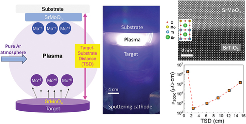
The cubic perovskite SrMoO3 with a paramagnetic ground state and remarkably low room-temperature resistivity has been considered as a suitable candidate for the new-era oxide-based technology. However, the difficulty of preparing single-phase SrMoO3 thin films by hydrogen-free sputtering has hindered their practical use, especially due to the formation of thermodynamically favorable SrMoO4 impurity. In this work, we developed a radio frequency sputtering technology enabling the reduction reaction and achieved conductive epitaxial SrMoO3 films with pure phase from a SrMoO4 target in a hydrogen-free, pure argon environment. We demonstrated the significance of controlling the target-to-substrate distance (TSD) on the synthesis of SrMoO3; the film resistivity drastically changes from 1.46 × 10⁵ μΩ·cm to 250 μΩ·cm by adjusting the TSD. Cross-sectional microstructural analyses demonstrated that films with the lowest resistivity, deposited for TSD = 2.5 cm, possess a single-phase SrMoO3 with an epitaxial perovskite structure. The formation mechanism of the conductive single-phase SrMoO3 films can be attributed to the plasma-assisted growth process by tuning the TSD. Temperature-dependent resistivity and Hall effect studies revealed metal-like conducting properties for low-resistive SrMoO3 films, while the high-resistive ones displayed semiconductor-like behavior. Our approach makes hydrogen-free, reliable and cost-efficient scalable deposition of SrMoO3 films possible, which may open up promising prospects for a wide range of future applications of oxide materials.
GRAPHICAL ABSTRACT
IMPACT STATEMENT
For the first time, we developed a plasma-assisted RF sputtering technology enabling the reduction reaction for the synthesis of single-phase conductive SrMoO3 epitaxial films from insulating SrMoO4 in pure-argon atmosphere.
Introduction
Transition-metal oxides (TMOs) with the perovskite structure (ABO3) provide an excellent platform for exploring exceptional transport properties arising from the interplay of charge, spin, orbital, and lattice degrees of freedom [Citation1–7]. The ongoing explosion of interest in TMO has led to an era of revolutionary inter-disciplinary research in spintronics, magnonics, and nano-engineering technology [Citation8–11]. While the 3d TMO received more attention than their 4d and 5d counterparts due to strong on-site Coulomb repulsion among the 3d electrons and ease of synthesis [Citation1–7,Citation12], recent studies on heavy metal based 4d TMOs like Ru and Ir oxides have been undertaken [Citation8–11,Citation13]. The 4d TMO systems are characterized by extended d orbitals leading to strong neighboring orbital hybridization, weak on-site Coulomb repulsion energy, high charge-transfer and crystal-field splitting energies [Citation14]. Pioneering studies on these systems have reported substantial spin-orbit coupling, large spin-Hall efficiency, high conductivity, and large carrier density, making them potential candidates for oxide-based electronic devices [Citation15–22]. Among 4d TMO compounds, SrMoO3 (SMO) has a cubic (Pmm) perovskite structure and behaves as a Pauli paramagnetic band metal [Citation14,Citation15,Citation17,Citation23–26]. The 4d-t2g orbital of tetravalent Mo cations in SMO consists of two unpaired electrons responsible for the n-type conduction mechanism [Citation27]. A low resistivity of 5.1 μΩ·cm at room temperature (RT) was reported in its bulk form [Citation23]. In view of its unique properties, SMO is one of the attractive candidates for applications in transparent conductors, microwave devices, and spintronic devices [Citation15,Citation17,Citation28,Citation29].
Nevertheless, the synthesis of monophasic SMO thin films remains a formidable challenge due to the formation of SrMoO4 (I4₁/a) as a secondary phase. The high conductivity of the SMO films is susceptible to the stabilization of the thermodynamically unfavorable Mo4+ state (4d2 valence configuration) near the Fermi level [Citation28]. It is particularly important to efficiently develop the synthesis parameters to be free of impurities in order to increase the conductivity of SMO films and to promote their widespread applications. Available reports on SMO indicate pulsed laser deposition (PLD) technique as its most popular synthesis method [Citation24,Citation26,Citation27,Citation30]. However, certain shortcomings such as restricted deposition area, particulate formation and high synthesis cost make PLD unsuitable for large-scale production. Radio frequency (RF) magnetron sputtering proves to be more effective as it enables uniform growth over large deposition substrates and has a high reproducibility rate [Citation31–33]. Previous reports on the preparation of sputter-deposited SMO films have shown that H2-Ar gas mixture is essential for single-phase SMO synthesis [Citation25,Citation34,Citation35]. However, the use of the H2 gas limits efficient scalable deposition for practical applications. Therefore, the development of an alternative sputtering technique that ensures the feasibility of low-cost, H2-free, large-scale SMO deposition is strongly desirable.
In this study, we developed an RF sputtering technique to fabricate conductive single-phase SMO epitaxial thin films using an insulating SrMoO4 ceramic target in pure Ar ambience. The use of a small target-to-substrate distance (TSD) of 2.5 cm, where the substrate is directly exposed to the RF plasma of the SrMoO4 target, successfully yielded single-phase SMO(001) with resistivity down to 250 μΩ·cm at RT via plasma assistance. Temperature dependence of the film resistivity and ordinary Hall effect revealed that the prepared low resistive SMO films exhibited metallic behavior characterized by high carrier concentration and moderate mobility.
Experimental methodology
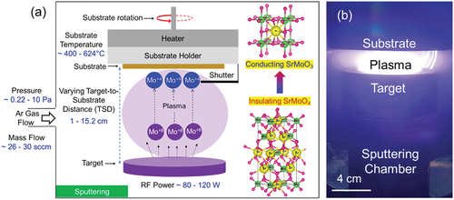
SMO thin films (~30 nm) were deposited on SrTiO3(STO)(001) substrates using an ultrahigh vacuum RF magnetron sputtering chamber with a rotating-substrate configuration at a base pressure of 1 × 10⁻⁷ Pa. The STO substrates were pre-baked at 800°C for 1 h in a muffle furnace to ensure a flat surface before SMO deposition. A schematic illustration of the sputtering chamber is shown in . A real-time image of the plasma emitted from a 3-inch-diameter SrMoO4 sintered target (Toshima Manufacturing Co. Ltd, Japan) is shown in . Pure Ar gas was used as the process gas for deposition. We investigated the sputtering parameters, including the input RF power, Ar pressure, substrate temperature, and TSD. The Sr:Mo atomic ratio in the thin films was confirmed using x-ray fluorescence technique (Rigaku Corporation, Japan; Model: ZSX Primus II). The crystal structures of the SMO films were characterized by in-situ reflection high energy electron diffraction (RHEED, manufactured by R-DEC Co. Ltd, Japan) and by ex-situ x-ray diffraction (XRD) techniques. Out-of-plane and in-plane XRD scans were performed on a SmartLab diffractometer from Rigaku Corporation, Japan, with Cu-Kα1 radiation and an incident Ge(220) monochromator. Atomic force microscopy (AFM) technique was used to probe the surface morphology and roughness by employing a scanning probe microscope manufactured originally by Seiko Instruments Inc., Japan. Cross-sectional microstructural analysis was performed using scanning transmission electron microscopy (STEM), with specimens prepared through a standard lift-out method utilizing focus ion beam (FIB) on a FEI Helios5UX scanning electron microscope (SEM): high-angle annular dark-field STEM (HAADF-STEM) imaging, energy dispersive X-ray spectroscopy (EDS) mapping and nano-beam electron diffraction (NBED) using a Cs-corrected FEI Titan G2 80–200 ChemiSTEM operated at 200 kV. Temperature dependence of the DC-electrical resistivity and Hall resistance from 50 K to 300 K were evaluated using the standard four-probe van der Pauw method with a physical property measurement system (VersaLab, Quantum Design, USA).
Figure 1. (a) A schematic illustration of the sputtering process employed in a sputtering chamber for deposition of SrMoO3 thin films from a SrMoO4 sintered target; (b) a photograph of the sputtering chamber during deposition with TSD of 2.5 cm.
Results and discussions
Thin film synthesis and film surface characterizations
A systematic optimization process was employed to determine the precise synthesis parameters for SMO thin films. Firstly, clean STO(001) substrates were subjected to a pre-deposition heat treatment at 800°C yielding a terrace surface morphology as shown in Fig. S1 of the Supplementary Information (SI), which is a prerequisite for high quality thin films. Next, we established the Ar pressure required to obtain the desired Sr:Mo stoichiometry ( = 1:1). The Sr/Mo atomic ratio in the SMO films as a function of the Ar pressure is shown in Fig. S2 of SI. We found that the Ar pressure of 10 Pa led to the desired Sr/Mo atomic ratio in the formed films. The optimum power for the least resistive SMO thin film was determined to be 100 W (see Fig S3). Further, an epitaxial growth of SMO films on STO(001) substrates could be attained only when the deposition temperature TS was maintained at 624°C, in comparison to depositions made at room temperature and 400°C. Hence, using this Ar pressure, RF power, and Ts during deposition, epitaxial SMO with (001) orientation was grown on a STO(001) substrate pre-baked at 800°C.
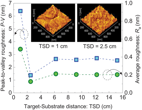
represent the typical RHEED patterns observed for the SMO films deposited at TSD = 1.0, 2.5, and 6.2 cm, respectively. The incident electron beam azimuths were parallel to the STO[100] and STO[110] directions. The RHEED patterns for other TSDs are shown in Fig. S3 of SI while that of the STO (001) substrate is also shown in Fig. S4. The narrow streaks observed in the patterns along both the azimuths clearly indicate (001) epitaxial growth of the SMO films. The longest streak patterns with the highest intensity were observed for the film deposited when TSD = 2.5 cm. depicts the graphical illustration of the TSD dependence of the peak-to-valley roughness (P-V, left axis) and the average surface roughness (Ra, right axis) of the films. The lowest P-V ~1.37 nm and Ra ~0.13 nm were achieved for TSD = 2.5 cm. The inset of shows 3-dimensional AFM images for TSD = 1.0 cm and 2.5 cm. We observed that the film for TSD = 1.0 cm exhibited particle agglomeration or growth of clusters which contributed to high values of P-V and Ra, while the film for TSD = 2.5 cm showed a uniform growth.
Figure 2. RHEED patterns for the surface of SMO (30 nm) films deposited at Ts = 624°C on STO(001) substrates with the incident electron beam parallel to (a)-(c) STO[100] and (d)-(f) STO[110] azimuth, respectively. (a) and (d) TSD = 1.0 cm, (b) and (e) 2.5 cm, and (c) and (f) 6.2 cm, respectively.
![Figure 2. RHEED patterns for the surface of SMO (30 nm) films deposited at Ts = 624°C on STO(001) substrates with the incident electron beam parallel to (a)-(c) STO[100] and (d)-(f) STO[110] azimuth, respectively. (a) and (d) TSD = 1.0 cm, (b) and (e) 2.5 cm, and (c) and (f) 6.2 cm, respectively.](/cms/asset/5d6339d9-6521-41f3-bd92-e4a178c13b1e/tsta_a_2378684_f0002_oc.jpg)
Figure 3. TSD dependence of P-V and Ra for SMO (30 nm) films. The inset shows AFM images for TSD = 1.0 cm and TSD = 2.5 cm.
Thin film structural characterizations
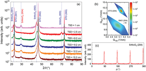
shows the out-of-plane XRD patterns of 30-nm-thick SMO films with various TSDs. We clearly observed Bragg reflections corresponding to SMO(001), SMO(002), and SMO(003) from all the films. However, except for TSD = 2.5 cm, additional peaks are observed at ~29.5º and ~61.2º, which are not assigned to the perovskite structure and could be attributed to the secondary phase of SrMoO4 belonging to the tetragonal I4₁/a space group. Moreover, as the TSD decreased from 15.2 cm to 6.2 cm, the peak intensity of SMO(00l) increased while the secondary peaks gradually reduced and finally vanished at TSD ~2.5 cm. Interestingly, when we further reduced the TSD to 1.0 cm, the secondary peak reappeared again. Thus, the TSD is the most crucial factor in obtaining single phase SMO films using pure Ar gas. The out-of-plane lattice parameter of the SMO film for TSD = 2.5 cm was calculated to be c ~0.404 nm which is slightly larger (~1.6%) than the bulk value, abulk = 0.3976 nm [Citation36]. exhibits the reciprocal space map (RSM) around the STO(204) Bragg reflection for TSD = 2.5 cm. The Q100 component of the SMO(204) Bragg peak is clearly observed and deviates from the peak of STO(204), indicating that the in-plane lattice parameters of the SMO film are not fully locked by the STO substrate. The estimated in-plane lattice constant of the least resistive SMO thin film was determined to be a ~0.396 nm, slightly lower than the c value (~0.404 nm). Furthermore, we evaluated the XRD in-plane scan (ϕ-scan) for the SMO(204) plane. represents the ϕ-scan profile of the film prepared at TSD = 2.5 cm, clearly showing the four-fold peaks expected for a cubic perovskite structure. From these results, we conclude that the single phase SMO film is epitaxially grown on a STO(001) substrate using Ar 10 Pa, TSD = 2.5 cm, and Ts = 624°C.
Figure 4. (a) Out-of-plane XRD patterns for various TSDs of SMO (30 nm) films. (b) RSM results around the STO(204) and SMO(204) reflections and (c) ϕ-scan pattern of the SMO(204) lattice planes for TSD = 2.5 cm and Ts = 624°C.
The cross-sectional microstructures of the SMO film with TSD = 2.5 cm and Ts = 624°C were characterized using STEM, as shown in . The low magnification HAADF-STEM image in reveals very sharp and smooth interfaces at the SMO/STO substrate. The NBED patterns obtained from the SMO film and STO substrate are shown in , respectively, with the viewing directions along SMO[100] and STO[100]. Therefore, the epitaxial relationship between SMO and STO was determined to be SMO(001)[100]//STO(001)[100]. The EDS maps in display the elemental distribution corresponding to the rectangular framed region in , indicating homogeneous distribution of each element in the SMO film, and no apparent elemental interdiffusion at the interface. The corresponding EDS line profiles shown in revealed that the Mo/Sr ratio in the SMO layer is close to 1, and the O signal remains unchanged from the STO to SMO region. The atomic-resolution HAADF-STEM image in exhibits an atomically flat SMO(001)/STO(001) interface. Since the HAADF contrast of the atomic column is nearly proportional to the square of the atomic number Z of the element (Z: 22 for Ti, 38 for Sr and 42 for Mo), the Sr atomic columns have a brighter contrast than that of Ti in STO, while the light element O (Z: 8) could not be clearly observed [Citation37,Citation38]. The intensity difference between Sr and Mo atomic columns in the SMO layer seems to be much smaller due to their similar atomic numbers. The schematic atomic model shown in the inset of illustrates a nearly perfect lattice matching at the SMO/STO interface. In addition, as shown in , the perfect lattice matching is further confirmed by the lattice outline image, which was obtained from the inverse fast Fourier transform (IFFT) image with masking {010} diffractions of the FFT image of as marked by dotted circles in the inset of . These microstructural analyses indicate the high quality of the SMO films obtained using RF sputtering in the pure Ar ambience with TSD = 2.5 cm. We also note that the RSM result shown in implies that the in-plane lattice parameters of the SMO film are not fully locked by the STO substrate, but HAADF-STEM images shown in imply lattice matching. These results indicate that the SMO film has an epitaxial strain (~1.4%) from the substrate around the interface, and it gradually relaxes with increasing the film thickness.
Figure 5. (a) Low magnification cross-sectional HAADF-STEM image of SMO film on STO(001) substrate. (b) and (c) are [001] NBED patterns acquired along SMO[100] and STO[100], respectively. (d) EDS maps collected from the region marked by a dashed-line rectangular frame in (a), and (e) corresponding EDS line profiles. (f) High magnification HAADF-STEM image near the SMO(001)/STO(001) interface. (g) IFFT filtered outline image of (f). The inset of (g) shows the FFT image of (f) and filter areas (dotted circles) for obtaining (g).
![Figure 5. (a) Low magnification cross-sectional HAADF-STEM image of SMO film on STO(001) substrate. (b) and (c) are [001] NBED patterns acquired along SMO[100] and STO[100], respectively. (d) EDS maps collected from the region marked by a dashed-line rectangular frame in (a), and (e) corresponding EDS line profiles. (f) High magnification HAADF-STEM image near the SMO(001)/STO(001) interface. (g) IFFT filtered outline image of (f). The inset of (g) shows the FFT image of (f) and filter areas (dotted circles) for obtaining (g).](/cms/asset/cca20d2d-9ef6-4a4f-a4af-64bc46760fb2/tsta_a_2378684_f0005_oc.jpg)
Electric transport properties
shows the TSD dependence of the RT resistivity (ρ300K) for the 30-nm-thick SMO films measured using the van der Pauw method. The SMO film for TSD = 2.5 cm exhibits the lowest ρ300K. The value of ρ300K significantly changes with TSD, decreasing dramatically from 1.46 × 10⁵ μΩ·cm for TSD = 15.2 cm to 310 μΩ·cm for TSD = 2.5 cm, while orders of magnitude increase to 1.98 × 10⁶ μΩ·cm for TSD = 1.0 cm is observed. The lowest ρ300K for TSD = 2.5 cm is comparable to the reported value for a SMO film deposited using PLD [Citation27] and is lower than the resistivity of SMO films previously grown by magnetron sputtering with hydrogen-containing plasma [Citation25,Citation35]. We also investigated the SMO thickness tSMO dependence of ρ300K in the range between 10 nm and 100 nm for TSD = 2.5 cm, as shown in . The ρ300K gradually decreases with increasing tSMO. When tSMO <20 nm, the ρ300K increases rapidly, almost doubling that of 100 nm. These results attribute the SMO film conductivity to the film region rather than the SMO/STO interface [Citation39,Citation40].
Figure 6. (a) TSD dependence of the resistivity at 300 K (ρ300K) of the SMO films, (b) ρ300K as a function of the SMO thickness for TSD = 2.5 cm. (c) temperature dependence of the resistivity: upper panel: TSD = 1.0 cm, lower panel: 2.5 cm, 6.2 cm and 15.2 cm. The green solid line of the upper panel indicates the fitting result of Equation (2). The red solid lines of the lower panel indicate fitting results using Equation (1).
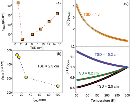
Next, we investigated the temperature ρT dependence of the resistivity ρ to unveil the underlying conduction mechanisms in the SMO films fabricated at different TSDs. shows the normalized plots of (T)/ρ300K versus temperature for different TSDs. The film with TSD of 2.5 cm exhibits the lowest resistivity over the entire T range. The ρ(T) for films deposited when TSD = 2.5 cm and 6.2 cm increases with decrease in ρT, exhibiting a metallic trend, similar to that of conductive SMO films deposited using PLD [Citation24,Citation27]. On the other hand, the films with TSD = 15.2 and 1.0 cm show a semiconductor-like behavior where ρ increases with T. We fitted the (T)/ρ300K vs. T plots of TSD = 2.5, 6.2 and 15.2 cm to the power law expression given as [Citation27],
where is related to the residual resistivity of the films, while A and B are the coefficients of the temperature dependent terms. The T and T2 terms represent the contributions of electron-phonon and electron–electron scatterings to the resistivity, respectively [Citation27]. The sign of A is important in determining the type of conduction; a positive sign represents the behavior of a metallic conductor, while a negative sign represents a semiconducting behavior. All the SMO films except for TSD = 1.0 cm were well fitted by EquationEquation (1)
(1)
(1) as shown in the lower panel of and the extracted fitting parameters are listed in . For the films for TSD = 2.5 cm and 6.2 cm, the parameter A is positive, indicating that the films exhibit metallic behavior. This is attributed to the delocalized d electrons in the Mo4+ valence state [Citation41–43]. In contrast, A of the film for TSD = 15.2 cm is negative, indicating a semiconductor-like behavior; this may be due to the presence of the SrMoO4 secondary phase.
Table 1. The fitting parameters , A, and B obtained from fitting in using Equation (1).
Since the resistivity for TSD = 1.0 cm is much higher than that for other TSDs, we used a combined model of two-dimensional Mott variable-range hopping (VRH) [Citation44] and electron-phonon scattering [Citation45] to describe its conduction behavior with the following equation:
where is the mathematical form of the VRH of localized carriers and
denotes the linear dependence of the resistivity on temperature due to electron-phonon scattering.
and
represent the relative contributions of the two mechanisms to the resistivity, respectively. T0 is 50 K, the lowest temperature in the experiment, and
is the temperature coefficient of the resistivity. The data for TSD = 1.0 cm were well fitted by EquationEquation (2)
(2)
(2) as shown in the upper panel of , suggesting a complex conduction mechanism for the film obtained at TSD = 1 cm. The values of fitting parameters were obtained to be
= 3.2,
= −0.25 × 10⁻⁴, and
= −4.6. The contribution of the Mott VRH mechanism to
is much larger (~104 order) compared to electron-phonon scattering phenomenon. In general, Mott VRH is more pronounced in disordered thin films, where localized electron motion dominates, resulting in an exponential temperature dependence of resistivity. Thus, the film deposited at TSD = 1 cm behaves as a highly disordered semiconductor system characterized by localized charge carrier states. In addition, the negative sign of
also confirms the semiconducting nature of the film. Thus, the studies of the temperature dependence of the resistivity provide evidence for a change in the conduction mechanism with TSDs.
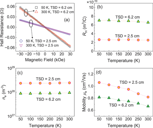
We further performed Hall measurements on the SMO films exhibiting a metallic behavior (TSD = 2.5 and 6.2 cm). The Hall voltages VH of the SMO films contain only the ordinary Hall effect contribution, which can be described by the following equation [Citation46]:
where RH is the Hall coefficient, I is the current, and tSMO is the film thickness (30 nm). RH can be extracted by calculating the slope from the study of the Hall resistance as a function of magnetic field H. The carrier concentration ne and mobility µe in the SMO film were obtained from the following relationships: ne = 1/RHe and µe = 1/neρ = RH/ρ, where e is 1.602 × 10⁻¹⁹ C and ρ is the resistivity at a given temperature. shows the transverse Hall resistance Rxy of the SMO films for TSD = 2.5 and 6.2 cm, which was measured under an out-of-plane magnetic field. Considering the geometry of our Hall measurement, we conclude that electrons are the dominant charge carriers for the conductive SMO films. show the temperature dependence of RH, electron concentration ne, and electron mobility µe, respectively. From these data, we observe that µe decreases with increasing temperature, while RH and ne exhibit a very weak temperature dependence. The decrease in µe can be understood as an increase in the amplitude of the lattice vibrations with increase in temperature, which leads to a higher susceptibility to carrier collisions and consequently results in a decrease in µe. The SMO film for TSD = 2.5 cm with the lowest resistivity exhibits a high ne value of ~2.5 × 1028 m−3, which is in good agreement with the theoretically calculated value of ~3.2 × 1028 m−3 for correlated 4d2 SMO thin films assuming a contribution of two 4d electrons per Mo to a unit cell [Citation15]. The maximum µe is ~1.1 cm2/Vs, which is also comparable to that of a PLD-deposited SMO film [Citation15].
Figure 7. (a) Out-of-plane magnetic field dependence of hall resistance at 50 and 300 K of the films for TSD = 2.5 and 6.2 cm. Temperature-dependences of (b) RH, (c) ne, and (d) μe.
Finally, we discuss the formation mechanism of the conductive single-phase SMO films by modulating the TSDs. The strong TSD dependence indicates a plasma-assisted SMO formation origin. The visible plasma for the optimum TSD = 2.5 cm at 100 W surrounds a volume of ~114 cm3 between a 3-inch target and the substrate. In the absence of a reducing atmosphere such as a H2 gas mixture, the thermodynamically stable SrMoO4 is converted to conductive SMO in the sputtering chamber by plasma assistance, i.e. 2SrMoO4 2SrMoO3 + O2. The efficiency of this conversion is closely related to the variation of TSD. The plasma-assisted growth associated with TSD was reported for the formation of a highly (001)-textured MgO barrier for CoFeB/MgO/CoFeB magnetic tunnel junctions [Citation47], but the mechanism was not yet clear. Here, the combination of a high Ar gas pressure ~10 Pa and RF power ~100 W (power density ~2.2 × 10⁻² W/mm2) could promote the ionization process of the process gas atoms: Ar → Ar+ + e–. The Ar+ ions accelerate and impinge upon the sputtering cathode, i.e. the SrMoO4 target, thus ejecting sputtered ions from it by collision. Subsequently, the ‘knocked off” electrons from the Ar atoms participate in the following reaction inside the plasma: Mo6+ +2e– → Mo4+. The conversion efficiency from Mo6+ to Mo4+ seems to increase progressively with decreasing TSD up to the optimum TSD value of 2.5 cm, as we demonstrated the change in intensity of the SrMoO4(004) impurity peak in the XRD pattern (see with varying TSD. The conversion efficiency reaches a maximum for TSD = 2.5 cm where no secondary phase is observed in the SMO film. A further decrease in TSD (1.0 cm) results in the reappearance of the SrMoO4 impurity peak, which may be due to (i) an increase of plasma damage into the film and (ii) a greatly enhanced sputtering rate (see Fig. S6) which results in a much shorter approach time from target to substrate compared to the plasma-assisted reduction reaction time.
Summary
Conductive epitaxial SMO thin films with a perovskite structure were successfully synthesized by using TSD controlled RF magnetron sputtering in a pure Ar atmosphere on STO substrates via plasma assistance. A small TSD of 2.5 cm resulted in a 30 nm thick film with a flat surface, small lattice mismatch with the substrate, no secondary phase formation, and a low resistivity of 310 μΩ·cm at RT. A series of TSD-dependent reactions in the plasma involving the target material and Ar gas assisted the prescribed strategy for sputter deposition in the absence of H2 in the process gas mixture, thus yielding pure phase epitaxial conductive films. Temperature dependence of the resistivity and Hall resistance shed light on the conduction mechanism of the SMO films deposited using different TSDs. For the lowest (1.0 cm) and highest TSD (15.2 cm), the prepared films exhibited semiconducting properties, while the SMO films deposited for TSD = 6.2 cm and 2.5 cm, the temperature dependence of the resistivity and Hall resistance revealed metallic behavior. SMO thin films hold promising future prospects due to their metallic conduction property and high carrier concentration which have garnered widespread interest in this material for applications in transparent conductive oxides, solid-state batteries, and photocatalysis. Additionally, ongoing research aims to explore the use of SMO in perovskite solar cells and oxide-based electronics. Therefore, achieving high-quality thin films with high RT conductivity through a H2-free sputtering technique is critical in enhancing the potential of SMO for next-generation electronic devices.
Supplemental Material
Download PDF (202.1 KB)Disclosure Statement
No potential conflict of interest was reported by the author(s).
Supplementary Material
Supplemental data for this article can be accessed online at https://doi.org/10.1080/14686996.2024.2378684
Additional information
Funding
References
- Lechermann F. Late transition metal oxides with infinite-layer structure: nickelates versus cuprates. Phys Rev B. 2020;101(8):081110. doi: 10.1103/PhysRevB.101.081110
- Rao CNR, Cheetham AK. Giant magnetoresistance in transition metal oxides. Science. 1996;272(5260):369–10. doi: 10.1126/science.272.5260.369
- Chen Z, Liu Z, Sun Y, et al. Two-dimensional superconductivity at the LaAlO3/KTaO3 (110) heterointerface. Phys Rev Lett. 2021;126(2):026802. doi: 10.1103/PhysRevLett.126.026802
- Moon SJ, Jin H, Kim KW, et al. Dimensionality-controlled insulator-metal transition and correlated metallic state in 5 d transition metal oxides Srn+1IrnO3n+1 (n=1, 2, and ∞). Phys Rev Lett. 2008;1 01(22):226402. doi: 10.1103/PhysRevLett.101.226402
- Tokura Y, Nagaosa N. Orbital physics in transition-metal oxides. Science. 2000;288(5465):462–468. doi: 10.1126/science.288.5465.462
- Biswas A, Jeong YH. Effects of substrate temperature on the unusual non-fermi liquid metal to insulator transition in perovskite SrIrO3 thin films. J Phys D Appl Phys. 2015;48(13):135303. doi: 10.1088/0022-3727/48/13/135303
- Mackenzie AP, Julian SR, Diver AJ, et al. Quantum oscillations in the layered perovskite superconductor Sr2RuO4. Phys Rev Lett. 1996;76(20):3786. doi: 10.1103/PhysRevLett.76.3786
- Wang S, Liu B, Zhu Y, et al. Enhanced performance of TiO2-based perovskite solar cells with Ru-doped TiO2 electron transport layer. Sol Energy. 2018;169:335–342. doi: 10.1016/j.solener.2018.05.005
- Qin M, Xiao Y, Yang H, et al. Ru/Nb co-doped perovskite anode: achieving good coking resistance in hydrocarbon fuels via core-shell nanocatalysts exsolution. Appl Catal B: Environ. 2021;299:120613. doi: 10.1016/j.apcatb.2021.120613
- Diaz-Morales O, Raaijman S, Kortlever R, et al. Iridium-based double perovskites for efficient water oxidation in acid media. Nat Commun. 2016;7(1):12363. doi: 10.1038/ncomms12363
- Shitade A, Katsura H, Kuneš J, et al. Quantum spin hall effect in a transition metal oxide Na2IrO3. Phys Rev Lett. 2009;102(25):256403. doi: 10.1103/PhysRevLett.102.256403
- Zaanen J, Sawatzky GA, Allen JW. Band gaps and electronic structure of transition-metal compounds. Phys Rev Lett. 1985;55(4):418. doi: 10.1103/PhysRevLett.55.418
- Corredor LT, Aslan-Cansever G, Sturza M, et al. Iridium double perovskite Sr2YIrO6: a combined structural and specific heat study. Phys Rev B. 2017;95(6):064418. doi: 10.1103/PhysRevB.95.064418
- Lee YS, Lee JS, Noh TW, et al. Systematic trends in the electronic structure parameters of the 4d transition-metal oxides SrMO 3 (M= Zr, Mo, Ru, and Rh). Phys Rev B. 2003;67(11):113101. doi: 10.1103/PhysRevB.67.113101
- Ha Y, Lee S. Oxygen‐Vacancy‐endurable conductors with enhanced transparency using correlated 4d2 SrMoO3 thin films. Adv Funct Mater. 2020;30(28):2001489. doi: 10.1002/adfm.202001489
- Stoner JL, Murgatroyd PA, O’Sullivan M, et al. Chemical control of correlated metals as transparent conductors. Adv Funct Mater. 2009;29(11):1808609. doi: 10.1002/adfm.201808609
- Salg P, Walk D, Zeinar L, et al. Atomically interface engineered micrometer-thick SrMoO3 oxide electrodes for thin-film BaxSr1-xTiO3 ferroelectric varactors tunable at low voltages. APL Mater. 2019;7(5). doi: 10.1063/1.5094855
- Onos Y, Tokura Y. Doping dependence of the anomalous hall effect in La1−xSrxCoO3. Phys Rev B. 2006;73(17):174421. doi: 10.1103/PhysRevB.73.174421
- Jadaun P, Register LF, Banerjee SK. Rational design principles for giant spin hall effect in 5d-transition metal oxides. Proc Natl Acad Sci USA. 2020;117(22):11878–11886. doi: 10.1073/pnas.1922556117
- Medvedeva JE. Magnetically mediated transparent conductors: In2O3 doped with Mo. Phys Rev Lett. 2006;97(8):086401. doi: 10.1103/PhysRevLett.97.086401
- Egbo KO, Adesina AE, Ezeh CV, et al. Effects of free carriers on the optical properties of high mobility transition metal doped In2O3 transparent conductors. Phys Rev Mater. 2021;5(9):094603. doi: 10.1103/PhysRevMaterials.5.094603
- Magyari-Köpe B, Tendulkar M, Park SG, et al. Resistive switching mechanisms in random access memory devices incorporating transition metal oxides: TiO2, NiO and Pr0.7Ca0.3MnO3. Nanotechnology. 2011;22(25):254029. doi: 10.1088/0957-4484/22/25/254029
- Nagai I, Shirakawa N, Ikeda SI, et al. Highest conductivity oxide SrMoO3 grown by a floating-zone method under ultralow oxygen partial pressure. Appl Phys Lett. 2005;87(2):024105. doi: 10.1063/1.1992671
- Wang HH, Cui DF, Zhou YL, et al. Growth and characterization of SrMoO3 thin films. J Cryst Growth. 2001;226(2–3):261–266. doi: 10.1016/S0022-0248(01)00799-0
- Mizoguchi H, Kitamura N, Fukumi K, et al. Optical properties of SrMoO3 thin film. J Appl Phys. 2000;87(9):4617–4619. doi: 10.1063/1.373111
- Zhu M, Li P, Hu L, et al. Thickness dependence of metal–insulator transition in SrMoO3 thin films. J Appl Phys. 2022;132(7):075303. doi: 10.1063/5.0098993
- Lekshmi IC, Gayen A, Hegde MS. The effect of strain on nonlinear temperature dependence of resistivity in SrMoO3 and SrMoO3−xNx films. Mater Res Bull. 2005;40(1):93–104. doi: 10.1016/j.materresbull.2004.09.004
- Salg P, Zeinar L, Radetinac A, et al. Oxygen diffusion barriers for epitaxial thin-film heterostructures with highly conducting SrMoO3 electrodes. J Appl Phys. 2020;127(6):065302. doi: 10.1063/1.5129767
- Radetinac A, Mani A, Melnyk S, et al. Highly conducting SrMoO3 thin films for microwave applications. Appl Phys Lett. 2014;105(11):114108. doi: 10.1063/1.4896339
- Wang HH, Yang GZ, Cui DF, et al. Epitaxial growth and electric characteristics of SrMoO3 thin films. J Vac Sci Technol A: Vac Surf Films. 2001;19(3):930–933. doi: 10.1116/1.1355756
- Lung C, Toma M, Pop M, et al. Characterization of the structural and optical properties of ZnO thin films doped with Ga,Al and (Al + Ga). J Alloys Compd. 2017;725:1238–1243. doi: 10.1016/j.jallcom.2017.07.265
- Lee J, Lee D, Lim D, et al. Structural, electrical and optical properties of ZnO: Al films deposited on flexible organic substrates for solar cell applications. Thin Solid Films. 2007;515(15):6094–6098. doi: 10.1016/j.tsf.2006.12.099
- Toma M, Marconi D, Pop M, et al. Influence of substrate-target distance on structural and optical properties of Ga and (Al+ Ga)-doped ZnO thin films deposited by radio frequency sputtering. Analytical Lett. 2019;52(14):2227–2238. doi: 10.1080/00032719.2019.1606819
- Inukai T, Murakami T. Preparation of conductive SrMoO3 thin films and their application to electrodes for thin film capacitors. Jpn J Appl Phys. 1985;24(S3):21. doi: 10.7567/JJAPS.24S3.21
- Ryu HU, Sun HJ. Preparation of conductive SrMoO3 thin films by RF magnetron sputtering and evaluation of their electrical conduction properties. J Korean Inst Electr Electron Mater Eng. 2011;24(6):468–472. doi: 10.4313/JKEM.2011.24.6.468
- Macquart RB, Kennedy BJ, Avdeev M. Neutron diffraction study of phase transitions in perovskite-type strontium molybdate SrMoO3. J Solid State Chem. 2010;183(1):250–255. doi: 10.1016/j.jssc.2009.11.005
- Hartel P, Rose H, Dinges C. Conditions and reasons for incoherent imaging in STEM. Ultramicroscopy. 1996;63(2):93–114. doi: 10.1016/0304-3991(96)00020-4
- He C, Li Z, Chen H, et al. Unusual solute segregation phenomenon in coherent twin boundaries. Nat Commun. 2021;12(1):722. doi: 10.1038/s41467-021-21104-8
- Namba Y. Resistivity and temperature coefficient of thin metal films with rough surface. Jpn J Appl Phys. 1970;9(11):1326. doi: 10.1143/JJAP.9.1326
- Barua S, Rajeev KP. Status of surface conduction in topological insulators. AIP Adv. 2014;4(1). doi: 10.1063/1.4864058
- Mizoguchi H, Fukumi K, Kitamura N, et al. Electronic structure of polycrystalline AMoO3 (A= Sr or Ba). J Appl Phys. 1999;85(9):6502–6505. doi: 10.1063/1.370288
- Wells MP, Zou B, Doiron BG, et al. Tunable, low optical loss strontium molybdate thin films for plasmonic applications. Adv Opt Mater. 2017;5(22):1700622. doi: 10.1002/adom.201700622
- Hopper HA, Le J, Cheng J, et al. An investigation of the optical properties and water splitting potential of the coloured metallic perovskites Sr1−xBaxMoO3. J Solid State Chem. 2016;234:87–92. doi: 10.1016/j.jssc.2015.12.002
- Gantmakher VF. Electrons and disorder in solids. Vol. 130. (NY) (NY): Oxford University Press; 2005.
- Russo U, Ielmini D, Cagli C, et al. Filament conduction and reset mechanism in NiO-based resistive-switching memory (RRAM) devices. IEEE Trans Electron Devices. 2009;56(2):186–192. doi: 10.1109/TED.2008.2010583
- Hall EH. On a new action of the magnet on electric currents. Am J Sci. 1880;3(111):200–205. doi: 10.2475/ajs.s3-19.111.200
- Choi GM, Shin KH, Seo SA, et al. Substrate biasing effect during MgO deposition in CoFeB/MgO/CoFeB MTJs. IEEE Trans Magn. 2009;45(6):2371–2373. doi: 10.1109/TMAG.2009.2018577