Abstract
Hydrogenated a-Si:H, first reported by the late professor Walter Spear, has found an application in solar cells and, via tremendous R&D efforts, a series of industrial technologies have been developed to produce large area thin film Si solar modules. Thin film Si:H solar modules began production in 1999 and became a major industry due to environmental concerns. Our proposed solar module is now the global standards. In this paper, the history of thin film Si solar cell technologies are reviewed.
1. Introduction
Thin film Si:H solar cell technologies are attracting considerable attention for the mass-production of large-area solar modules. Since the first report of the valence electron control of hydrogenated amorphous silicon by Spear and LeComber Citation1, numerous studies have been carried out on amorphous Si:H solar cells to improve efficiency, reliability and productivity. A more recent development has been the supply of turn-key systems to photovoltaic (PV) module manufacturers throughout the world. In general, thin Si:H film PV modules are based on the a-SiC:H/a-Si:H heterojunction solar cell structure developed by Tawada et al. Citation2. Hydrogenated amorphous SiC:H (a-SiC:H) was first reported by Anderson and Spear Citation3, who demonstrated that a-SiC:H showed a wide band gap but the valence electrons were not controlled. To improve the efficiency of p-i-n a-Si:H solar cells, we attempted to control the valence electrons and, in 1981, good controllability was achieved in hydrogenated a-SiC:H prepared by plasma decomposition of a gaseous mixture of silane and methane. We applied this p-type a-SiC:H with a band gap of 2.0 eV to the window-side p-layer of an a-Si:H solar cell, i.e. an a-SiC:H/a-Si:H heterojunction solar cell Citation4, and improved its efficiency to 8% in 1982 Citation5. The a-SiC:H/a-Si:H heterojunction solar cell was initially commercialized as an electrical power supply for several types of consumer electronics. To utilize the cell for grid-connecting photovoltaic applications, several problems have had to be overcome, such as module efficiency, the Stabler–Wronski effect, long-term stability, mass-production technologies and cost competitiveness. It took more than 15 years to achieve the installation of these photovoltaic systems in private houses.
In 1993, subsidies for PV modules were introduced in Japan, mainly using crystalline silicon solar modules. The PV market has continued to expand but module costs need to be reduced significantly to realize its full commercial potential. The development of thin film Si solar modules was crucial in the growing market for grid-connecting photovoltaics; thus, we decided to focus our R&D strategy on thin film photovoltaic modules based on the following strategy:
Materials: safety → silicon | |||||
Structure: simple structure → single pin junction | |||||
Efficiency: cost performance → stable 8% | |||||
Cost goal: less than poly-crystalline silicon module → Min. 40 MW/year | |||||
Deadline for mass-production: by the year 1999. | |||||
Next-generation technology of thin crystalline Si:H technologies with 12% efficiency to be introduced by the year 2003.
Following this stratagem, we established a series of mass-production technologies for a-Si:H modules by 1998 and invested $65 million in a new subsidiary production company, Kaneka Solartech, with a 20 MW/year production capacity, which was established in Toyooka City, Hyogo Prefecture. We began shipping a-SI:H modules in October 1999, increasing capacity to 40 MW/year in 2004. Regarding the next-generation technology, we developed an a-Si:H/thin film poly-Si:H tandem (hybrid) solar cell and established a 10% module technology in 2000. For successful marketing of PV systems for roof-tile applications in Japan, a module efficiency of at least 10% is required to provide a 3-kW PV system. We introduced a new chemical vapor deposition (CVD) system for thin film poly-Si:H layers in the Toyooka Plant for the production of the hybrid module, and began producing the 10% hybrid module in April 2001. We are continuing to improve the efficiency of the hybrid module using an a-Si:H/intermediate layer/thin poly-Si:H structure, and to develop a high-throughput CVD system for thin poly-Si:H. In 2006, we developed a 12% technology for the a-Si:H/intermediate layer/thin poly-Si:H hybrid module, but required two more years to establish the required high-throughput production technologies. We successfully began mass production of the 12% hybrid module in 2008.
2. Valence electron control of a-SiC:H and its application to solar cells
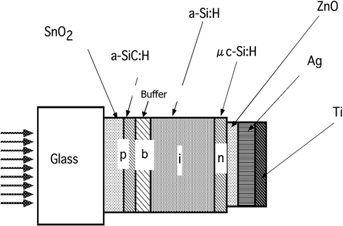
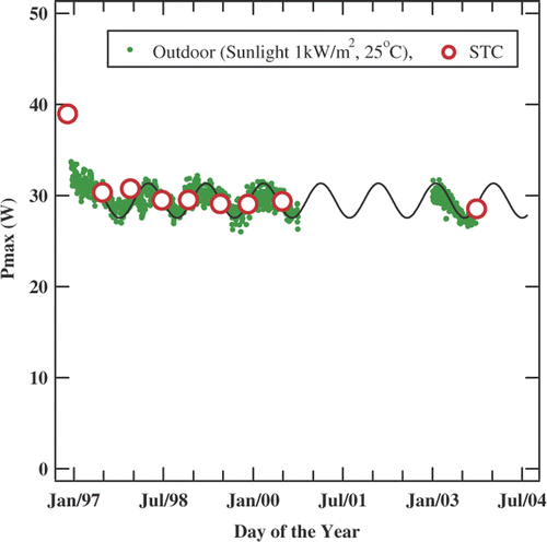
Hydrogenated a-SiC:H was first reported by Anderson and Spear Citation3 and data on the effect of impurity doping on the basic properties of a-SiC:H were published by Tawada and Hamakawa Citation2. Our investigations showed that methane-based a-SiC:H is almost entirely constructed with tetrahedrally coordinated carbon or carbon bonded to hydrogen, and is superior to ethylene-based a-SiC:H films for use as a window material in p-i-n a-Si:H solar cells. Initially, we observed a photoconductivity recovery effect on impurity doping in methane-based a-SiC:H with an optical band gap of <2.1 eV. Boron-doped methane-based a-SiC:H showed a larger photoconductivity, by one or two orders of magnitude, compared to undoped material. using IR and Auger electron spectroscopy, we concluded that methane-based a-SiC:H with an optical band gap of <2.1 eV is an ideal amorphous SiC:H alloy Citation4. We applied this methane-based a-SiC:H to p-i-n a-Si:H solar cells as the p-layer, and developed a high-efficiency a-SiC:H/a-Si:H heterojunction solar cell technology Citation5. The structure of a typical device is shown in . Through several optimizations, an initial efficiency of 11% and stabilized efficiency of 8.5% for a 100 × 100 mm area cell was obtained in 1992. To further improve efficiency, a double junction using a-Si:H Citation6 and a-SiGe:H, and a triple junction Citation7 were proposed. We investigated the cost/performance relationships between these structures, and concluded that a single junction of a-SiC:H/a-Si:H was the most practical structure for obtaining a low-cost solar module for terrestrial power applications. Consequently, we pursued the realization of large-area solar modules, leading to the development of a 1.2 × 1.2 m electrode CVD apparatus and large-area laser pattering systems in 1994. The dimensions of the glass substrate having a SnO2 electrode were 910 × 910 mm in area and 4 mm thick. We improved the uniformity of the cell performance by optimizing the deposition conditions and increased the effective cell area by decreasing the lost area for electrical integration via laser processing. Through this optimization process, the highest initial module efficiency of 10.6% was obtained with an I sc of 1.26 A, V oc of 42.5 V, FF of 73% and P max of 39.1 W in 1995 Citation8.
Figure 1. Schematic of the a-SiC:H/a-Si:H heterojunction solar cell structure.
The key issues at this time were how to control the Staebler–Wronski effect (light-soak degradation) and how to certify module efficiency. shows the performance change of the a-Si:H module at 38°C under strong light irradiation (70 mW/cm2). The module performance degreases by 20% within 100 h and appears stabilized until 4500 h. The Japan Quality Assurance Organization (JQA) carried out field tests on our modules in Australia and Japan, starting in 1996. The light-soak degradation of a-SiC:H/a-Si:H single junction modules is strongly dependent on the module temperature and ambient conditions. As shown in , the module performance decreases in winter and recovers in summer, and this change is reversible. The same effect was recorded in Perth () and in Darwin (), Australia. We concluded that the average light-soak degradation of our modules is less than 18% in Japan. Regarding long-term reliability, JQA also estimated the lifetime of a-Si:H modules by accelerated simulation under conditions of strong light-soaking and annealing Citation9. The results in suggest that a-Si:H solar modules would be stable for about 30 years after the initial degradation.
Figure 2. Performance change in a-Si:H module at 38°C under 70 mW/cm2 irradiation.
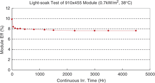
Figure 3. Field exposure tests on the a-Si:H module in Hamanako by JQA since August 1997.
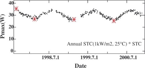
Figure 4. Long-term reliability field test on a-Si:H modules over a seven-year period in Perth, Australia.
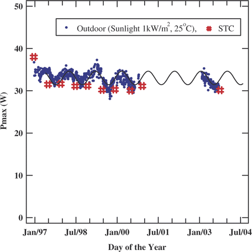
Figure 5. Long-term reliability field test on a-Si:H modules over a seven-year period in Darwin, Australia.
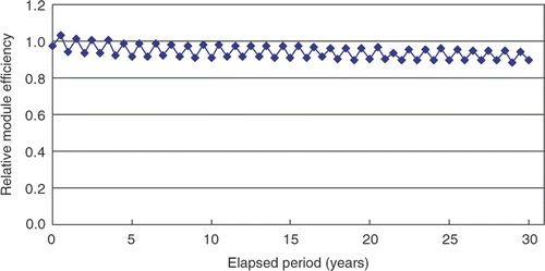
Figure 6. Long-term stability simulation of a-Si:H cell (as the standard of a one-year light-soaked cell).
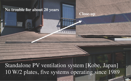
The author installed our a-Si:H modules on his house from 1989 and, as shown in , these modules are continuing to generate electricity after nearly 20 years of service. This proves that our a-Si:H modules have a photovoltaic lifetime of at least 20 years.
Figure 7. Solar roofing tiles of a-Si:H solar module installed in 1989 on a private house.
3. Mass-production of a-Si:H modules
In parallel with developing the technology of large-area, stable 8% a-Si:H modules, we also investigated the most cost-effective production scale and concluded the capacity to be 40 MW/year, consisting of two lines of 20 MW/year CVD production. To realize this strategy, we developed 20 MW/year of CVD, sputtering and laser patterning systems for a substrate size of 1 × 1 m. In 1998, we constructed a pilot production line with 4 MW/year capacity at our Shiga Plant to confirm the specifications of each item of equipment, module performance and production yield. We produced the modules in the Shiga pilot-plant using a low-cost SnO2 substrate, achieving an average module efficiency of 9.2%. It was concluded that a-Si:H modules can compete with c-Si modules from the viewpoint of production cost, with a production scale of more than 40 MW/year. In September 1998, we invested $65 million in a 20 MW/year production plant in Toyooka City, Hyogo Prefecture, where Kaneka Solartech Corporation was established as a subsidiary of Kaneka as 100% shareholder Citation10. Here, we began producing commercial a-Si:H modules with a size of 980 × 910 mm and performance of 64 W. Since 2004, the PV market has expanded enormously owing to the success of political pressure for PV technology in Germany. However, a shortage of Si feedstock became a serious problem for the production of c-Si PV modules. Due to these market conditions and the Si feedstock problem, thin film PV modules and, especially, a-S:Hi solar modules are now attracting considerable attention from system integrators and PV newcomers. We increased our production capacity to 24 MW/year in 2003, 40 MW/year in 2006, 55 MW/year in 2007 and 75 MW/year in 2008, and will increase our capacity at the Toyooka site to 150 MW/year by 2010. It has taken a quarter of a century since the invention of the a-SiC:H/a-Si:H heterojunction solar cell for the success of the a-Si solar cell to finally bloom, with the result that it is now one of the global standard thin film PV structures.
4. State-of-the-art of the next generation of thin film technologies
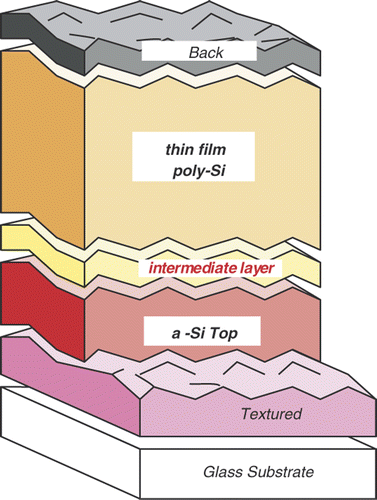
The a-Si:H solar module cannot sustain its competitiveness against other technologies indefinitely. Yamamoto et al. Citation11 developed a low-temperature process for deposition of thin film crystalline Si in 1993 and achieved 9.8% efficiency for a thin film c-Si:H solar cell with a 3 µm thickness. To further improve efficiency, a further increase in thickness is required, which would introduce new problems such as high cost and internal stress within the films. We proposed a new hybrid cell structure comprising a-Si:H and thin film c-Si:H (), taking advantage of a thinner layer of thin film c-Si:H. This hybrid cell showed a stable 12% efficiency during the initial trial stages. One major advantage is that we can easily alter the a-Si:H module production line by adding a glow discharge deposition chamber for thin film c-Si:H layers. In addition, since this hybrid module can be integrated using a laser-scribing process, similarly to the a-Si:H module, the equipment for a-Si module fabrication can be easily utilized.
Figure 8. Schematic of the a-Si:H/thin film c-Si:H hybrid solar cell structure.
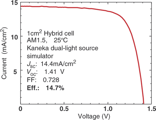
The hybrid technology was introduced into the Toyooka Plant in 2002, enabling commencement of production of stable 10% hybrid modules. We subsequently continued to improve the hybrid module efficiency, achieving a 12% technology in 2004 Citation12. Our target year for introducing 12% modules into the marketplace was originally 2005. But, to produce these commercially, we had to develop a high-throughput production system in-house, since the thickness of the thin film c-Si:H layer is 10 times that of the a-Si:H layer. This took a few years, with the result that, in 2008, we began partial production of 12% modules in our Toyooka Plant and will increase the production level from now. As regards further improvements, a 14.7% efficiency was obtained, as shown in , with a 1-cm2 cell by inserting the intermediate transparent layer between the a-Si:H top cell and the thin film c-Si:H bottom cell. We expect our proposed cell structure will be a significant module with high efficiency in near future.
Figure 9. V–I characteristics of the 14.7% small area cell.
The PV market continues to show enormous expansion and many newcomers have joined the field of thin film solar module production. Recently, a number of equipment suppliers have started shipping turn-key production systems for a-Si:H modules to newcomers. Total production capacity of the turn-key systems is estimated to be more than 1000 MW/year by 2010, with a subsequent increase to 4850 MW/year by 2013. Almost all of these thin film Si:H solar modules have the same structure as our a-SiC:H/a-Si:H heterojunction module. These turn-key equipment suppliers also intend to ship systems for fabricating similar modules to our hybrid structure. It is not easy to maintain the long-term reliability of thin Si:H solar modules, but we have developed our technologies through numerous acceleration and field tests on improved modules for long-term reliability. A worrying problem is that, if the modules produced by these newcomers give reliability problems in future, the confidence which we have built up within the thin Si:H film community would suffer. We, therefore, strongly request that manufactures confirm the reliability of their modules before shipping. The late Professor Walter Spear also made a wish for further evolution of thin Si:H solar module technologies and production.
Acknowledgements
R&D on thin Si:H films and solar cells in Japan has been supported by the New Energy Development Organization as the New Sunshine Project under METI. I would like to thank the members concerned.
References
- Spear , WE and LeComber , PG . 1976 . Phil. Mag. , 33 : 935
- Tawada , Y , Tsuge , K , Kondo , M , Okamoto , H and Hamakawa , Y . 1982 . J. Appl. Phys. , 53 : 5273
- Anderson , DA and Spear , WE . 1977 . Phil. Mag. , 35 : 1
- Tawada , Y , Okamoto , H and Hamakawa , Y . 1981 . Appl. Phys. Lett. , 39 : 2378
- Hamakawa , Y and Tawada , Y . 1982 . Int. J. Sol. Ener. , 1 : 125
- S. Arya, D.E. Carlson, L. Yang, L.F. Chen, F. Willing, K. Rajan, K. Jansen, J. Newton and T. Komero, Technical Digest of the 9th International Photovoltaic Solar Energy Conference, Arisumi, Japan, 11–15 November (1996), p.279
- S. Guha, J. Yang, A. Banerjee, T. Glafelter and S. Sugiyama, Technical Digest of the 9th International Photovoltaic Solar Energy Conference, Arisumi, Japan, 11–15 November (1996), p.283
- Kondo , M , Nishio , H , Kurata , S , Hayashi , K , Takenaka , A , Ishikawa , A , Nishimura , K , Yamagishi , H and Tawada , Y . 1997 . Sol. Ener. Mater. Sol. Cell. , 49 : 1
- Tawada , Y and Yamagishi , H . 2001 . Sol. Ener. Mater. Sol. Cell. , 66 : 95
- Tawada , Y , Yamagishi , H and Yamamoto , K . 2003 . Sol. Ener. Mater. Sol. Cell. , 78 : 647
- Yamamoto , K , Suzuki , T , Kondo , K , Okamoto , T , Yamaguchi , M , Izumina , M and Tawada , Y . 1994 . Sol. Ener. Mater. Sol. Cell. , 34 : 501
- Tawada , Y . 2008 . Technology Management (F&I) , 2 : 121 [in Japanese]