Abstract
This introductory paper to the special conference marking the retirement of Professor David Cockayne gives a brief outline of his career. It highlights some of his many seminal contributions in research, and also refers briefly to his outstanding contributions to the promotion, dissemination and teaching of electron microscopy not covered in the scientific programme of the conference.
Keywords:
1. Introduction
David Cockayne retired from his Professorship in the Physical Examination of Materials at Oxford University at the end of September 2009. This is an important milestone and is an appropriate occasion to pay tribute to his past achievements. This special issue consists of papers presented at a conference organised in his honour in Oxford on 7 September 2009. The topics of this conference are within the main scientific areas in which David made seminal advances: (1) the weak beam technique of electron microscopy of defects, (2) applications of electron diffraction to the study of amorphous and crystalline materials, and (3) the characterisation of nanoscale structures and interfaces.
David Cockayne was born in London in 1942, and he and his parents emigrated to Australia when he was eight years old. He has joint Australian and British nationality and it is clear from his brief Curriculum Vitae at the end of this paper that there has been a strong attraction to both countries throughout his career, leading to oscillations from one to the other. In this introduction, we first follow his research career in approximately chronological order, and attempt to describe the nature of his research, referring briefly to a few of the many seminal contributions he has made. In a later section, we comment on the outstanding contributions he has also made to the promotion, dissemination and teaching of electron microscopy, not covered in the scientific programme.
2. Research career (until 2009)
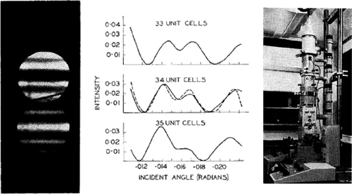
David began research in electron diffraction in 1964 in Melbourne, working with Peter Goodman, Alex Moodie and John Cowley (). The project was to test the multislice theory of electron diffraction Citation1. It involved the construction of a precision convergent beam electron diffraction camera and the calculation of the intensity distribution as a function of incident angle, using the Cowley–Moodie theory, to compare with the observed intensity distribution in the convergent beam electron diffraction pattern from MoS2 (see ). This was the first test of the multislice theory and enabled the thickness of the specimen to be determined to within one unit cell. The research is described in Citation2. In the course of this work, David discovered that the original Cowley–Moodie equations in Citation1 included an incorrect sign, i.e. that it was effectively a theory of positron diffraction.
Figure 1. Professor D.J.H. Cockayne FRS.
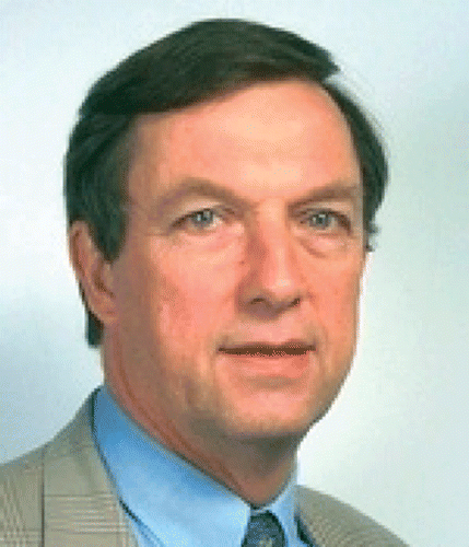
Figure 2. Professor A.F. Moodie, Dr P. Goodman, and Professor J.M. Cowley.
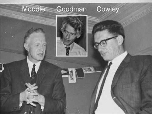
Figure 3. Comparison of experimental and calculated intensities as a function of incident angle for the 100 reflection in MoS2 Citation2. Reprinted with permission from Review of Scientific Instruments, D.J.H. Cockayne, P. Goodman, J.C. Mills and A.F. Moodie, Design and operation of an electron diffraction camera for the study of small crystalline regions, Vol. 38, Issue 8, p. 1097, Copyright 1967, American Institute of Physics.
This project had a considerable influence on David's approach to his subsequent research. It involved high precision measurements and rigorous in-depth theoretical analysis of the results. These are the hallmarks of David's research portfolio.
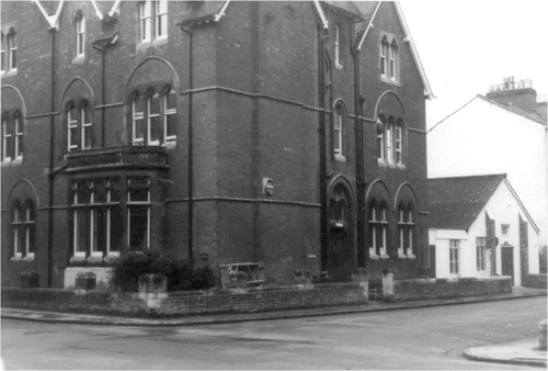
In 1966, David was awarded a Commonwealth Scholarship and he moved to Oxford to the Department of Metallurgy to carry out research towards a D.Phil., supervised by M.J. Whelan. shows a youthful Cockayne amongst the members of the Department in 1967. At the time, the electron microscopes were housed in the hut next to the house at 10 Parks Road (), which served as the Metallurgy Annex, and most of the electron microscopists had their offices in the house. Number 10 Parks Road used to be the Mathematical Institute and during the war it served as a Maternity Hospital. They were referred to by the metallurgists in the main Metallurgy (Hume-Rothery) building as “unfrocked physicists and chemists”. There was a close community spirit among the occupants of 10 Parks Road, but David and his wife Jean fostered the community spirit in the Department as a whole by organising walks in the Oxfordshire countryside.
Figure 4. David Cockayne in 1967 in the laboratory photograph of the Department of Metallurgy, University of Oxford.
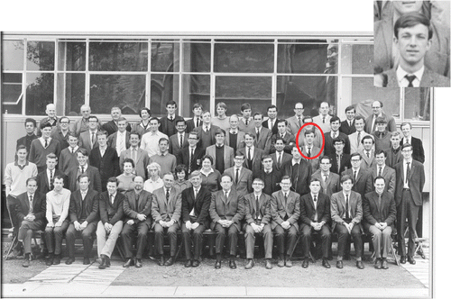
Figure 5. Metallurgy Annex at 10 Parks Road. Electron microscopes were housed in the hut.
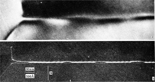
The object of David's research project was to probe the strain-field close to the cores of dislocations. He was introduced to the Howie–Whelan treatment of the dynamical theory of electron diffraction and its application to imperfect crystals Citation3. The result was the development (with Mike Whelan and Ian Ray) of the darkfield “weak beam” technique, which improved by an order of magnitude (to 1.5 nm) the resolution at which complex lattice defect geometries could be studied Citation4. The technique has had an important impact in advancing our understanding of the structure and properties of lattice defects in many materials, and became a routine tool used in laboratories all over the world. Forty years later, this technique is still widely used and some 20 or so papers using this technique are still published annually in major journals. Using this technique, David demonstrated unambiguously for the first time that glide dislocations in elemental semiconductors are dissociated into two partial dislocations bounding a stacking fault, thus settling a controversy which existed at the time, and determined accurate values of the stacking fault energies both in semiconductors and other materials. shows a climbing dislocation in Si imaged in dark-field in (a) and (b) in the same reflection, but at the reflecting position in (a) and in the weak beam condition in (b) (taken from Citation5). The large improvement in resolution in (b) is immediately apparent. Later, in Sydney, with Hons and Spence he showed that, in CdS, the dislocations moved in the dissociated form Citation6. He and his group went on to study misfit dislocations in strained layer heterostructures (InGaAs/GaAs system), and explained the structures observed in terms of elasticity theory Citation7. The development of the “weak beam” technique is discussed in Mike Whelan's paper in this issue.
Figure 6. Climbing dislocation in Si imaged in dark-field (a) at the reflecting position and (b) in the weak beam condition Citation5. Reprinted from I.L.F. Ray and D.J.H. Cockayne, Proceedings of the Royal Society A, Vol. 325, p. 543, , 1971, with permission from The Royal Society.
David spent part of 1970 at Chalk River as a Visiting Scientist to work with Parsons and Hoelke, who had interpreted perturbations in lattice fringe images, such as local bending or terminating fringes, in terms of dislocations. This assumed a one-to-one correspondence between fringe distribution and lattice plane distribution. David carried out image calculations using the Bloch wave formulation of the dynamical theory of electron diffraction for imperfect crystals Citation3 for inclined screw dislocations in thin foils, and showed that the number and nature of terminating fringes depend on the diffraction geometry, and that the assumption referred to above is not valid. This led to an important joint publication with Parsons and Hoelke Citation8.
In 1974, David returned to Sydney University to take up the appointment of Director of the Electron Microscope Unit. His research there covered a broad range of topics; in particular, the study of strain relief by misfit dislocations at interfaces in semiconductor heterostructures. He also branched out into a rather different area – the study of amorphous materials by electron diffraction. With McKenzie, he developed a powerful electron diffraction technique within an electron microscope to determine accurate radial distribution functions (giving the average distributions of atoms around a central atom) from small volumes of amorphous material, orders of magnitude smaller than possible with X-rays or neutrons due to their small scattering cross-sections Citation9. By collecting highly calibrated energy selected electron diffraction patterns to high scattering angles, he created a precision tool giving nearest-neighbour distances accurate to 0.001 nm. An early application was the first proof of the existence of thin film amorphous carbon in diamond form Citation10.
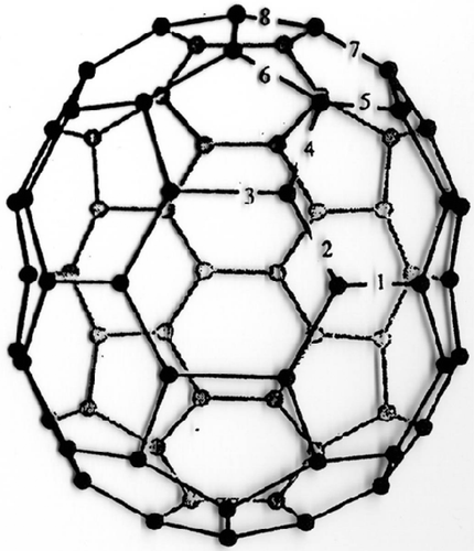
The thin amorphous carbon films were produced by deposition onto a NaCl substrate from a plasma stream of a cathodic vacuum arc with a curved magnetic filter. shows the diffracted intensity as a function of q, the smooth curve f2 fitted to it at high scattering angles, the reduced density function G(r) (closely related to the radial distribution function) as a function of interatomic distance r and a model of two linked tetrahedra of carbon atoms. The dotted vertical lines in the G(r) diagram indicate the interatomic distances in crystalline diamond. The two peaks corresponding to interatomic distances between first and second nearest neighbours are well reproduced in the amorphous carbon, while the peak of the third nearest neighbour is absent, corresponding to a random rotation of the two tetrahedra about the bond (2–5) linking them. Another example is the structure of the C70 molecule, which was obtained from the G(r) data for a powder sample using a simulated annealing technique, which assumes that the atoms interact through a potential equal to −G(r). The relaxed minimum energy structure is shown in taken from Citation11; it is an ellipsoidal-shaped molecule, slightly pinched at the waist, consisting of hexagons and pentagons of carbon atoms. The various interatomic distances within the molecule are determined to an accuracy of 0.001 nm.
Figure 7. RDF analysis of thin film amorphous carbon. See text for details. Image created by D.J.H. Cockayne.
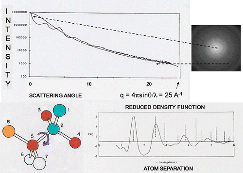
Figure 8. Structure of the C70 molecule from RDF data Citation11. See text for details. Reprinted by permission from Macmillan Publishers Ltd.: Nature, The structure of the C70 molecule, D.R. McKenzie, C.A. Davies, D.J.H. Cockayne, D.A. Muller and A.M. Vassallo, Vol. 355, p. 622, Copyright 1992.
David also started a research programme on quantum dots (QD), using TEM under zone axis multibeam imaging conditions, to obtain information on the composition, shape and size of the QDs, important in determining their optoelectronic properties. shows an example of the work of his group on coherent InGaAs QDs grown on an (001) GaAs substrate Citation12. The experimentally observed images, shown at the top of the composite diagram, consist of crosses with arms that spread out towards the periphery. The simulated images (a), (b) and (c), shown below the experimental images, are for lattice mismatches of 4, 6 and 7%, respectively. The strain-field distribution was calculated using three-dimensional anisotropic finite element analysis. The TEM image simulations were carried out using multi-beam dynamical theory with the column approximation Citation3. The arms of the cross in all three simulations have constant width. The simulation image (d) was calculated assuming a gradual increase of the mismatch from 4% at the bottom of the QD to 6% at the top. The arms of the cross now increase towards the periphery of the image, in qualitative agreement with experiment. This indicated segregation of In towards the surface of the QD.
Figure 9. Comparison of experimental and simulated [001] zone axis images of InGaAs quantum dots on a GaAs substrate, indicating surface segregation of In. See text for details. Image created by D.J.H. Cockayne.
![Figure 9. Comparison of experimental and simulated [001] zone axis images of InGaAs quantum dots on a GaAs substrate, indicating surface segregation of In. See text for details. Image created by D.J.H. Cockayne.](/cms/asset/92fb7090-3a2d-41d8-a398-2bcb1bd5b1ad/tphm_a_439909_o_f0009g.gif)
David returned to Oxford in 2000 to take up the post of Professor in the Physical Examination of Materials in the Department of Materials. He again built up a powerful research group. An important advance was the extension of the electron diffraction technique to obtain high precision data from nanosized volumes of amorphous materials Citation13. A recent application of this technique was the study of the structure of the rapid phase change material GeSbTe. This is described in the contribution by Borisenko et al. in this special issue.
The work on QDs also continued and, following the TEM evidence of elemental segregation at the surfaces, David and his group then showed by atomistic modelling that elemental segregation within QDs is an important strain-relief mechanism (in addition to previously accepted mechanisms), and developed a capability to carry out sophisticated modelling of QD structures in strained environments Citation14. This is described in the paper by Lang in this issue. A collaborative project with Frances Ross led to exciting real time observations of GeSi/Si (001) island shrinkage due to surface alloying during Si capping Citation15.
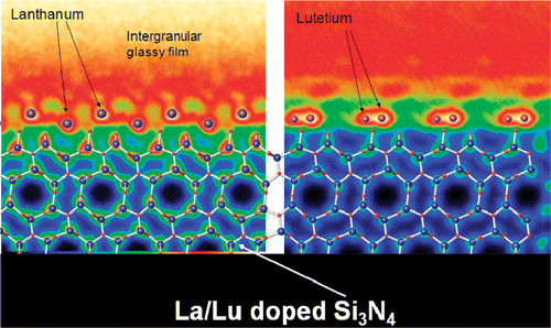
Another recent highlight of the research of David's group, in collaboration with a group in the University of Karlsruhe, was the determination of the positions of rare-earth doping atoms at the interface between crystalline Si3N4 and the amorphous intergranular films in this polycrystalline ceramic. The rare earth atoms La and Lu promote the growth of needle-like grains which enhance toughness. Using the high-angle annular dark-field (HAADF) STEM technique, David and his collaborators determined the three-dimensional coordinates of the specific sites of the La and Lu atoms relative to the adjacent Si3N4 crystal structure Citation16. shows the arrangements of the La and Lu atoms in the HAADF STEM images. The atoms at the corners of the hexagons are Si. The regular arrangement of the rare earth atoms within an otherwise amorphous layer is remarkable.
Figure 10. High-angle annular dark-field STEM images of La and Lu doping atoms in intergranular glassy film between Si3N4 grains. See text for details. Image created by D.J.H. Cockayne.
David's scientific work is characterised by a profound insight into the complexities of electron diffraction and microscopy, the development and application of high precision techniques and a rigorous analysis and deep understanding of experimental observations. Anyone who has been privileged to work with him knows that nothing but complete understanding will satisfy him. An important objective of his research has been to extract numbers from his observations, whether it is the separation of partials in a dissociated dislocation, accurate interatomic distances, precise positions of atoms, or chemical composition on a nanometre scale.
3. Promotion, dissemination, teaching and leadership of electron microscopy
David has also made outstanding contributions to the promotion, dissemination and teaching of electron microscopy. During his period in Sydney (1974–2000), he organised or promoted numerous courses and workshops on different aspects of electron microscopy and analysis, and was much respected for inspiring the younger microscopists and for stimulating interest in electron microscopy in schools. With H. Hashimoto, he promoted the Asia Pacific Conferences in Electron Microscopy and associated workshops.
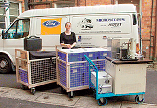
David was also keen to show school children the “hidden world” revealed by electron microscopy. He initiated in Sydney a scheme in which a table top SEM was loaned to schools for periods of two months for hands-on use by students and teachers. This developed into a “Microscopes on the Move” programme in which a specially adapted SEM could be transported in a dedicated van to schools across the country (). This programme got under way in 2000 after David had left Sydney, and was accessed by some 20,000 students, teachers and members of the public in the first year Citation17. Recently in the UK, David and Angus Kirkland have developed the Cyber SEM technique which enables schools to access and drive remotely an SEM in Oxford. This programme is now operating and many schools have expressed interest in taking part. These educational activities demonstrate David's enthusiasm for electron microscopy and the microscopic world, and his passion to enable the young and old to discover the secrets and beauty of this hidden world.
Figure 11. Microscopes on the move! Image created by D.J.H. Cockayne.
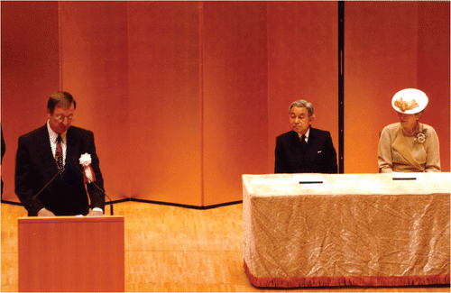
Finally, David has provided outstanding leadership for the electron microscope community. He was General Secretary of the Committee of Asia Pacific Societies of Electron Microscopy from 1984 to 1996. In 1995, be became General Secretary of the International Federation of Societies for Electron Microscopy (IFSEM), served as its President from 2003 to 2007, and is now vice-President till 2010. This illustrates his high standing internationally in the field. shows David in his capacity as President of IFSEM giving the opening address at the 16th International Microscopy Congress in Sapporo in 2006, in the presence of the Emperor and Empress of Japan. He also founded the Australian Key Centre for Microscopy and Microanalysis at the University of Sydney, and was Foundation President of the Australian Society for Electron Microscopy (1986–1988).
Figure 12. Cockayne delivering the opening address at the 16th International Microscopy Congress, Sapporo 2006, in the presence of the Emperor and Empress of Japan.
4. Conclusion
David Cockayne has had a wide-ranging and lasting impact in electron microscopy through his outstanding research, his promotion of the field through his inspired teaching and dissemination of the subject, and through his exemplary leadership. We wish him well in his well-earned retirement.
Acknowledgements
I am grateful to David Cockayne for providing me with much information on this paper, and to him and Jean Cockayne for the figures.
References
- Cowley , JM and Moodie , AF . 1957 . Proc. Phys. Soc. Lond. , 71 : 533
- Cockayne , DJH , Goodman , P , Mills , JC and Moodie , AF . 1967 . Rev. Sci. Instrum. , 38 : 1097
- Hirsch , PB , Howie , A , Nicholson , RB , Pashley , DW and Whelan , MJ . 1965 . Electron Microscopy of Thin Crystals , London : Butterworths .
- Cockayne , DJH , Ray , ILF and Whelan , MJ . 1969 . Phil. Mag. , 20 : 1265
- Ray , ILF and Cockayne , DJH . 1971 . Proc. R. Soc. Lond. A , 325 : 543
- Cockayne , DJH , Hons , A and Spence , JCH . 1980 . Phil. Mag. A , 42 : 773
- Zou , J and Cockayne , DJH . 1995 . Appl. Phys. , 77/76 : 2448
- Cockayne , DJH , Parsons , JR and Hoelke , CW . 1971 . Phil. Mag. , 24 : 139
- Cockayne , DJH and McKenzie , DR . 1988 . Acta Crystallogr. A , 44 : 870
- McKenzie , DR , Muller , DA , Kravtchinskaia , E , Segal , D , Cockayne , DJH , Amaratunga , G and Silva , R . 1991 . Thin Solid Films , 206 : 198
- McKenzie , DR , Davis , CA , Cockayne , DJH , Muller , DA and Vassallo , AM . 1992 . Nature , 355 : 622
- Liao , XZ , Zou , J , Cockayne , DJH , Leon , R and Lobo , C . 1999 . Phys. Rev. Lett. , 82 : 5148
- McBride , W , Cockayne , DJH and Nguyen-Manh , D . 2003 . Ultramicroscopy , 96 : 191
- Lang , C , Cockayne , DJH and Nguyen-Manh , D . 2005 . Phys. Rev. B , 72 ( 15 ) : 155328
- Lang , C , Kodambaka , S , Ross , FM and Cockayne , DJH . 2006 . Phys. Rev. Lett. , 97 : 226104
- Winkelman , GB , Dwyer , C , Hudson , TS , Nguyen-Manh , D , Döblinger , M , Satet , RL , Hoffmann , MJ and Cockayne , DJH . 2005 . Appl. Phys. Lett. , 87 : 061911
- O’Connor , C . 2008 . 50 Great Moments, Celebrating the Golden Jubilee of the University of Sydney's Electron Microscope Unit , Edited by: Ratinac , KR . 250 Sydney : Sydney University Press .
5. Brief curriculum vitae of D.J.H. Cockayne FRS
| Date and Place of Birth | = |
19 March 1942 London |
| Nationality | = |
Australian and British (Emigrated to Australia at age of eight) |
| Marital Status | = |
Married, two daughters, one son |
| 1964 | = |
B.Sc. 1st class Honours, University of Melbourne |
| 1966 | = |
M.Sc. 1st class Honours, University of Melbourne Research with Cowley, Moodie and Goodman |
| 1966–1969 | = |
Commonwealth Scholarship to read for D.Phil at Oxford. Supervisor M.J. Whelan |
Appointments and Honours
| 1969–1974 | = |
Research Fellow at Department of Metallurgy & Science of Materials, Oxford |
| 1974–Jan 2000 | = |
Director, Electron Microscope Unit, University of Sydney |
| 1995–Jan 2000 | = |
Director, Australian Key Centre for Microscopy and Microanalysis |
| Jan 2000–2009 | = |
Professor in the Physical Examination of Materials, University of Oxford |
| 2000–2009 | = |
Honorary Professor, School of Physics, University of Sydney |
| 2005 | = |
Honorary Professor, University of Science and Technology, Beijing |
| 1999 | = |
FRS |
| 2009 | = |
Massey Medal of Australian and UK Institutes of Physics |
Committees
| 1984–1996 | = |
General Secretary, Committee of Asia Pacific Societies of Electron Microscopy |
| 1995–2002 | = |
General Secretary, International Federation of Societies for Electron Microscopy (IFSEM) |
| 2003–2007 | = |
President, IFSEM |
| 2007–2010 | = |
Vice President, IFSEM |
| 1986–1988 | = |
Foundation President, Australian Society for Electron Microscopy |
Conferences, Workshops, etc. Organised
| 1975–1991 | = |
Chairman and Organiser, Biennial Vacation Schools on Electron Microscopy, Sydney |
| 1976 | = |
Chairman and Organiser, Fourth Australian Conference on Electron Microscopy, Sydney |
| 1984 | = |
Chairman and Organiser, Workshop on Electron Microscopy, Singapore (Australian Development Assistance Bureau) |
| 1988 | = |
Chairman and Organiser, Workshop on Electron Microscopy, Bangkok |
| 1990 | = |
Chairman and Organiser, Drummond Workshop in Analytical Electron Microscopy, Sydney |
| 1991–1994 | = |
Chairman and Organiser, Annual Training School on Maintenance and Operation of the EM, Sydney |
| 1995–1996 | = |
Chairman, Australian Conference on EM, Sydney |
| 2003 | = |
Organiser, EMAG Advanced School, Oxford |
| 2003 | = |
Convener, UK Delegate to BCEIA 2003, China |
| 2004 | = |
Organiser, Oxford–Princeton Summer School on Advanced Microscopy and Microanalysis |
| 2008 | = |
Organiser, Royal Society Discussion Meeting: “New possibilities with aberration corrected EM” |