
 ?Mathematical formulae have been encoded as MathML and are displayed in this HTML version using MathJax in order to improve their display. Uncheck the box to turn MathJax off. This feature requires Javascript. Click on a formula to zoom.
Abstract
A fundamental knowledge and understanding of the adhesion behaviour of metal–polymer systems is important as interface failure leads to a complete breakdown of flexible devices. A combination of in situ atomic force microscopy for studying topological changes and in situ synchrotron based stress measurements both during film tensile testing were used to estimate the adhesion energy of a thin bilayer film. The film systems consisted of 50–200 nm Cu with a 10 nm Cr adhesion layer on 50 μm thick polyimide. If the Cu film thickness is decreased to 50 nm the Cr interlayer starts dominating the system behaviour. An apparent transition from plastic to predominantly brittle deformation behaviour of the Cu can be observed. Then, compressive stresses in the transverse direction are high enough to cause delamination and buckling of the Cr interlayer from the substrate. This opens a new route to induce buckling of a brittle interlayer between a ductile film and a compliant substrate which is used to determine the interfacial adhesion energy.
1. Introduction
Flexible electronics such as paper-like displays and flexible skin sensors are of major interest for industrial applications [Citation1–3]. But the manufactured material systems consist of complicated single and multilayer structures on polymer substrates with submicron film thickness dimensions which may alter the mechanical properties compared to the well-known bulk behaviour. Therefore, the research on the mechanical, electrical and adhesion properties of thin film systems becomes more important to produce reliable and bendable devices with a long lifetime.
The fabricated systems can include multiple thin film materials; commonly used are ceramics [Citation4], glasses [Citation5,6] or metals, like aluminium [Citation7], gold [Citation8,9] or copper [Citation10,11] on flexible polymer substrates, such as polyimide (PI) [Citation9,11,12], polyethylene terephthalate [Citation5,6,13] or polydimethyl siloxane [Citation14,15]. It is known that the adhesion between pure copper films on polymer substrates is too weak to fabricate reliable devices that can suffer different mechanical conditions such as bending, tensile and compressive forces, without delamination of the film. Therefore, interlayers of titanium, chromium or tantalum with only a few nanometers in thickness are utilized [Citation16–19] to improve the adhesion strength between the metal film and the polymer substrate. If for example Cr is used as an interlayer between a Cu film and PI, the Cr interlayer reacts with the PI and forms a strong Cr–C bonding with the C atoms of the polymer [Citation20,21]. Unfortunately, these interlayers are rather brittle.
If thin brittle films on polymers are strained in tension, channel cracks will form perpendicular to the straining direction and at higher strains buckles (localized delamination) can form parallel to the straining direction if laterally compressive stresses occur [Citation12,13,19,22]. Cordill et al. presented a model which allows the calculation of the interfacial adhesion energy using only the geometry (width and height) of the formed buckles [Citation23]. Even though the buckles will form easily in strained brittle films, they are seldom observed in ductile films (Cu, Au) often used in flexible electronic devices due to their high electrical conductivity.
The main goal of this study is to establish a method to obtain the adhesion energy of a metallic bilayer film system with a brittle interlayer between a ductile metal film and a compliant substrate. Therefore, bilayers composed of 50–200 nm Cu/10 nm Cr on PI substrates are strained in situ under an atomic force microscope (AFM) to study the evolution of the crack as well as the localized surface deformation (neck) spacings. Furthermore, the AFM images are used to measure the buckle geometry which is required for the determination of the adhesion energy with the Fischer model as presented in reference [Citation23] by Cordill et al. In situ tensile tests analysing the Cu film stress by the synchrotron based sin²ψ diffraction technique are used to measure the stress evolution in the Cu film perpendicular to the straining direction. Thus, it is possible to investigate the Cu film stress necessary to cause buckling and interface delamination of the Cu film from the polymer substrate.
2. Experimental
In this study, thin films consisting of 50, 100 and 200 nm thick Cu and a 10 nm thick Cr adhesion layer on cleaned 50 μm thick PI substrate (brand: UPILEX) were investigated. The metal films were deposited by electron beam evaporation in a Balzers BAK 550 evaporation machine using a vacuum of 5 × 10⁻⁷ mbar and a deposition rate of 0.5 nm/s. To provide information about the microstructure of the Cu films, the grain sizes were measured using different electron microscopy techniques. The grain size of the 200 nm Cu film was determined by electron back scatter diffraction (EBSD) in a JEOL 6500 scanning electron microscope (SEM). Prior to the EBSD studies the sample was Argon ion polished for 20 min to remove the native oxide layer, and then sputtered with 2 nm carbon to minimize the sample drift due to the electron beam interaction with the non-conductive polymer substrate. The 200 nm Cu film shows a bimodal grain structure composed of approximately 1 μm large (1 0 0) grains embedded in smaller (1 1 1) grains with a size of around 100 nm. The microstructure of the thinner Cu films were investigated in a Philips CM 20 transmission electron microscope (TEM) at 200 kV accelerating voltage. The TEM samples were produced by a scrape technique for thin films [Citation24] where the Cu films were carefully removed from the polymer substrate using a cleaned razor blade. The metal fragments were then positioned on a conventional TEM grid for powders with a carbon membrane. The grain sizes of the thinner films were determined by measuring the horizontal grain diameter of at least 40 grains. The average grain size of the 50 nm thick Cu film is 36 ± 12 nm and for the 100 nm Cu film 65 ± 21 nm.
In this research, two different in situ straining experiments were used and the samples were cut with a scalpel to the dimensions of 7 mm × 35 mm (see insert of Figure ). In the first tensile tests, the samples were strained stepwise to 15–20% using a displacement controlled screw driven straining device which can fit under a Digital Instruments DI 3100 AFM [Citation25]. The engineering strains were calculated using the initial gauge length, which is around 18 mm, and the elongation after each straining step measured with calibrated calipers. Consecutive AFM images of approximately the same area were taken in tapping mode with a scan rate of 1 Hz, a resolution of 512 lines and a size of 25 μm × 25 μm to determine the density and spacing of the channel cracks and the localized deformation (thinning, necking) which formed during straining. Analysing if an AFM height profile feature is caused by cracking or necking is done by the method proposed in [Citation25] which is based on the ratio between the depth, Δ and the film thickness, h. If the ratio is greater than 0.15, a channel crack exists and otherwise a neck [Citation25].
The detection limit of this technique depends on the used AFM tip. In the experiments, NanosensorsTM PointProbe® Plus-NCHR with a tip radius of about 7 nm, a tip height of 10–15 μm and a macroscopic half cone angle of 20° are used. That means if the crack opening is small, the AFM tip cannot detect the bottom of the crack due to the taper of the tip, so that the crack will be observed as a small drop from the surface and not as a large drop in the height profiles. Therefore, the technique was first applied on brittle films with a large crack opening where the crack depth was 10–15% of the film thickness [Citation26].
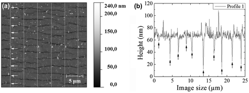
A line intercept method was utilized on the recorded images at every straining step to evaluate the crack and neck density. Six height profiles were taken on each AFM image and the number of cracks or necks which intercept with the lines were counted. The average densities are then the number of cracks or necks per line length averaged over the six lines. Furthermore, the distances between the cracks or necks were measured on every line and averaged over the six height profiles leading to one average crack spacing or one average neck spacing for each strain. Figure (a) shows an example of the six height profiles on an AFM image of the 50 nm thick Cu film at 16% strain where no necks are observed. Additionally, Figure (b) shows the corresponding plot of the height against the image size for profile 1 in which the cracks are marked with black arrows.
Figure 1. (a) AFM height image of the 50 nm Cu film at 16% strain with six lines from which the height profiles were taken. The white arrows indicate the intercept points with the cracks. (b) Corresponding height profile of Profile 1 from (a). The distances were measured between the cracks indicated by black arrows. No necks were observed in this film.
At higher strains, buckles can form parallel to the straining direction and perpendicular to the cracks (Figure (a)). The geometry of these buckles allows for the calculation of the adhesion energy (energy release rate) of thin films on polymer substrates with the model described in [Citation23]. Only the values of the half buckle width, b and the buckle height, δ, are needed normalized by the film thickness, h and plotted in the form of (δ/h)1/2 against (b/h) using the following equation [Citation23](1)
(1)
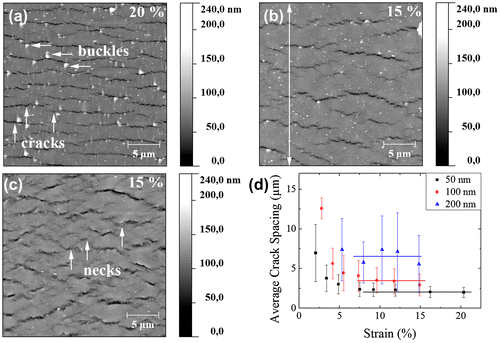
Figure 2. (colour online) AFM images of strained (a) 50 nm, (b) 100 nm and (c) 200 nm Cu films. The white arrow in (b) indicates the tensile direction for all images. (d) Average channel crack spacings of 50, 100 and 200 nm thick Cu films. The channel crack saturation range is indicated by straight lines to guide the eye.
with α as the only fitting parameter. The interfacial adhesion energy, Γ, can now be calculated with the knowledge of α using Equation (Equation2(2)
(2) )
(2)
(2)
where E′ is the modified elastic modulus, E′ = E/(1 – ν²). The model together with Equations (Equation1(1)
(1) ) and (Equation2
(2)
(2) ) and a description of the technique can be found in detail in [Citation23].
The second in situ straining experiments were performed in the KMC-2 beam line [Citation27] at the synchrotron BESSY II in Berlin, Germany, using a commercial Anton Paar 600 TS® straining device. The samples were strained in uniaxial tension to 12% with a loading rate of 0.1 mm/min and unloaded to a load of 0 N. The force and displacement of the film–substrate system allowing the calculation of the engineering stress and strain were recorded during the experiment. The common sin²ψ method [Citation28] was used to obtain the copper lattice strains perpendicular to the tensile direction in the films (see insert of Figure ) during the whole tensile test to monitor the film stresses leading to buckling of the film. The set-up was in reflection geometry with a beam wave length of 0.177 nm and a beam size of 300 μm. The intensities of the (1 1 1) copper peak were measured continuously at four different ψ angles with a Bruker VÅNTEC detector using an exposure time of 5 s (200 nm film) and 10 s (50 and 100 nm films) during the complete loading and unloading cycles. The film stresses were calculated using the sin²ψ method applying a Hill model and the X-ray elastic constant (1/2 S2) [Citation29] for an untextured (1 1 1) copper reflection in the transverse sample direction. The stresses in the Cu films obtained by the x-rays were registered simultaneously to the engineering stresses of the complete material system obtained by the load cell.
3. Results
The deformation behaviour of various Cu film thicknesses strained to 15–20% is very different. The AFM images (Figure (a)–(c)) show that the plastic deformation in the 200 nm Cu film is more pronounced than in the thinner films due to the high amount of necking in the thicker Cu film, and the channel crack patterns change from straight to zig-zag shaped channel cracks with increasing film thickness. The average channel crack spacings of the different film thicknesses against the engineering strains are shown in Figure (d). The channel crack spacings of the 50 and 100 nm Cu films decrease with increasing strain until a plateau is reached. These plateaus, indicated by straight lines, define the channel crack saturation range where new cracks will no longer form and only the cracks themselves widen with increasing strain. However, the 200 nm Cu film exhibits a nearly constant channel crack spacing independent of the strain. The error bars in this case are larger due to the low amount of channel cracks which could be evaluated in the 25 × 25 μm images. The mean values of the channel crack spacings at saturation are 2.2 ± 0.2 μm, 3.3 ± 0.2 μm and 6.6 ± 0.8 μm for the 50, 100 and 200 nm films, respectively. From Figure (a)–(c) it can be concluded that the amount of channel cracks decreases and the average channel crack spacings increase with increasing film thickness. Simultaneously, the amount of necking, i.e. localized plasticity, is reduced if the film thickness decreases, leading to buckling of the thinnest film due to lateral compressive stresses that build up. The buckles were first observed at 15–16% strain.
It is possible to determine the adhesion energy for the 50 nm Cu film with the adhesion model described earlier [Citation23]. The plot of (δ/h)1/2 against (b/h) is shown in Figure a with the minimum α value of 4 × 10⁻⁴. The minimum α value and the buckle geometry of the buckle tail is used in the calculation of the interfacial adhesion energy, because the model is only valid in the first stages of buckling, i.e. the ideal buckle geometry without cracks at the buckle top and with a symmetric cross-section.
Figure 3. (colour online) (a) Plot of (δ/h)1/2 against (b/h) with the fit of the minimum α value of 4 × 10⁻⁴. (b) SEM image of a FIB cross-section through a buckle showing delamination of the Cr–PI interface. The dashed white line indicates the PI surface.
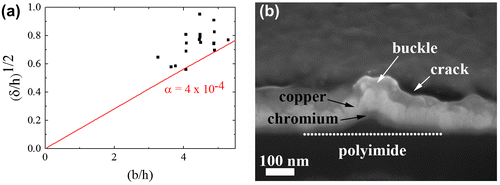
Focused ion beam (FIB) cuts through buckles of the 50 nm Cu film show that the weakest point in this material system is the Cr–PI interface where the bilayer begins to delaminate from the PI substrate (Figure (b)). However, for the determination of the adhesion energy the material constants of Cu (E = 128 GPa, ν = 0.36 [Citation16]) and Cr (E = 279 GPa, ν = 0.21 [Citation23]) are utilized with a compound film thickness of 60 nm, because the influence of the 50 nm Cu film is very strong compared to the influence of the 10 nm Cr interlayer. Therefore, the material parameters were weighted in the calculation, i.e. 5/6 of Cu and 1/6 of Cr. For a serial connection of the material parameters, the calculated interfacial adhesion energy of the 50 nm Cu/10 nm Cr bilayer film system was 6.3 J/m² with an error of ±0.8 J/m² determined by an α value of ±0.5 × 10⁻⁴ while a very similar value of 5.7 ± 0.7 J/m² is obtained assuming a parallel connection of the films. The latter value will be used for further discussion as the parallel connection describes the buckling condition in the best way.
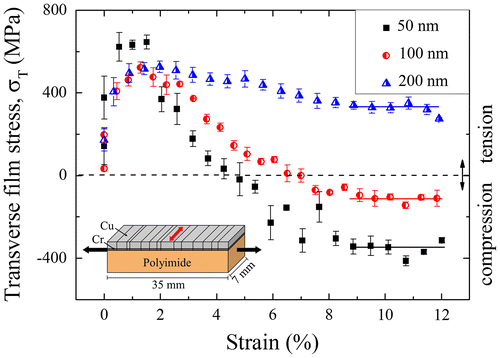
The stress measurements perpendicular to the straining axis (transverse film stress) show the unexpected formation of tensile stresses at low strains (Figure ). After a maximum tensile stress at 2% strain, the tensile stresses in the transverse direction decrease slightly for the thickest film, but more significantly for the thinner 100 and 50 nm thick films. In both cases the formation of compressive stresses can be observed.
Figure 4. (colour online) Film stresses of the 50, 100 and 200 nm Cu films against the engineering strain perpendicular to the straining direction. The error bars are calculated using the standard deviation. The dashed line indicates the transition from the compressive into tensile region and the solid straight lines the channel crack saturation ranges. A sketch of the cracked film system is inserted where the Cu film is drawn in light grey and the Cr film in dark grey. The tensile direction is indicated by black arrows and the measuring direction of the film stresses (transverse direction) by the red arrow.
4. Discussion
The transverse film stresses (see Figure ) show an increase of tensile stresses at low strains until the maximum peak stresses which correspond to the first deformation with cracking or necking. Thereby, the stress evolution can be explained by the model proposed by Frank et al. [Citation19] which estimates the mean coating stresses in straining and transverse direction based on basic considerations. In this study, Cu is expected to deform plastically at low strains leading to a lateral constriction (apparent Poisson’s ratio) of 0.5. However, PI shows a Poisson’s ratio of 0.32 as measured within this study. This explains (in good agreement with the model of Frank et al.) the unexpected formation of tensile stresses in the transverse direction at the beginning of the tensile test. The formation of channel cracks at 2% strain leads to a stress relaxation in straining direction and, in some cases, a transition of the tensile stresses to compressive stresses in transverse direction. For the 50 nm thick film, the compressive stresses are approximately –400 MPa which is sufficient to cause buckling perpendicular to the cracks and parallel to the tensile direction. In the case of the 100 nm thick film, compressive stresses form but are too low to induce buckling; in the case of the thickest film (200 nm), the transverse film stress is lower, but still well in the tensile regime which forbids buckling.
The stress evolution of the 50 nm (see Figure ) and 100 nm thick films is in good agreement with the model provided by Frank et al. [Citation19], even though the magnitude of tensile stresses is underestimated and of compressive stresses is overestimated by their approach. However, the 200 nm thick film does not show the predicted behaviour. This is mainly due to the fact that the thickest film shows a considerable amount of necking instead of channel cracking which does not lead to a significant stress reduction in either measured direction. It needs to be mentioned, that the validity of Frank`s model [Citation19] brakes down in such highly ductile films with a mixture of cracking and necking.
Figure 5. (colour online) Transverse film stresses of the 50 nm Cu film (in black) compared to the data evaluated by the model of Frank et al. [Citation19] (in red). A Poisson’s ratio of 0.36 for Cu and 0.32 for PI as well as the experimental data of the crack spacings are used in the model to calculate the stresses.
![Figure 5. (colour online) Transverse film stresses of the 50 nm Cu film (in black) compared to the data evaluated by the model of Frank et al. [Citation19] (in red). A Poisson’s ratio of 0.36 for Cu and 0.32 for PI as well as the experimental data of the crack spacings are used in the model to calculate the stresses.](/cms/asset/67e157cb-c7b4-40dd-ad2c-0f34715e88e0/tphm_a_920543_f0005_oc.gif)
The film thickness effect here is obvious. Besides the constraint of the plastic deformation by dislocation activity due to geometrical limitations of the film thickness and the grain size leading to a high yield strength [Citation30], also the brittle behaviour of the thin Cr interlayer affects the deformation behaviour on the Cu top layer considerably.
To validate and prove the results determined by the adhesion model of Cordill et al. [Citation23] for a bilayer Cu–Cr film system on PI, the model of Hutchinson and Suo [Citation31] for spontaneous buckling is used. Therefore, the critical buckling stress, σb, and the driving stress of the film, σd, are first calculated in consideration of the film thickness, h and the buckle geometry (buckle height, δ and buckle width, b) leading to the determination of the mixed mode interfacial fracture energy, Γ(Ψ), with the phase angle of loading, Ψ, using Equation (Equation3(3)
(3) ) [Citation31].
(3)
(3)
To compare the mixed mode interfacial fracture energy, Γ(Ψ), with the interfacial adhesion energy, Γ, the values were calculated for the same three buckles which achieved the requirements of Fischer’s model [Citation23] and thus could be fitted with the minimum α value. The value of Γ(Ψ) is 4.1 ± 0.4 J/m² for the parallel connection of the material parameters (4.5 ± 0.5 J/m² for the serial assumption) and lies in the same range of the interfacial adhesion energy calculated using Fischer’s model (Γ = 5.7 ± 0.7 J/m²). In this study, the standard deviation of the used method can be caused by the fact that the validity of the model is only ensured if the sample behaves pure elastically. However, it cannot be completely excluded that the 50 nm Cu/Cr sample did not deform with a low amount of plasticity, because the thicker films show a high amount of plastic deformation in the form of necking.
If the calculated interfacial adhesion energy of 5.7 J/m² (parallel connection) will be compared to other results found in literature, the values correspond also well with the adhesion energy of a bare Cr film on PI which was determined to 4.5 J/m² using the same technique and model [Citation23]. In this case, the Cr film starts buckling at approximately 10% strain, while compared to the investigated Cu/Cr film which delaminates at around 15% strain and shows a better adhesion strength than bare Cr films on polymer substrate that is also reflected in the larger adhesion value. Furthermore, the calculated adhesion energies correlate well with the interfacial energy between a chromium interlayer and a PI substrate consisting of a 300 nm Au/5 nm Cr film on PI [Citation32]. In this reference, the interfacial energy was approximately 7.3 J/m² determined by a four-point bending test.
Cordill et al. showed in strained 100 and 200 nm thick Cu films with 10 and 30 nm thick Ti interlayers on PI, that buckles form at 7 or 14% strain after annealing at 350 °C for 1 h due to a reduction of the adhesion by interdiffusion and intermetallic phase formation between Cu and Ti [Citation16]. The early buckling of this film system due to the microstructural and chemistry changes during annealing leads to a low adhesion energy of 0.2 J/m² and 0.25 J/m² [Citation16]. It can be observed that the Ti interlayer fails before the Cr interlayer due to a low bonding of this film system to the polymer which can also be concluded from the adhesion energy of 3.5 J/m² of a bare 50 nm Ti film on PI [Citation18]. Therefore, the usage of Cu–Cr film systems should be preferred over Cu–Ti film systems to produce reliable devices. In addition, Cu/Cr are not miscible and do not form brittle intermetallics while Cu/Ti are known to form intermetallic phases upon annealing [Citation33–35].
5. Conclusions
By decreasing the film thickness of Cu films, the amount of plastic deformation can be reduced and buckles will form due to lateral compressive stresses. These compressive stresses in the Cu films measured by in situ synchrotron experiments are only found for the 50 nm Cu/10 nm Cr film system to be high (–400 MPa) enough to induce buckle driven delamination of a buried Cr adhesion layer. Furthermore, a transition from plastic to rather brittle behaviour with decreasing film thickness was found where the Cr interlayer dominates the fracture and deformation behaviour. This is revealed by the different film stress evolution perpendicular to the straining direction as measured by synchrotron radiation. Additionally, the 200 nm thick films showed localized necking and channel cracking while only channel cracks were detected for the 50 nm thick films.
The adhesion model described in [Citation23] for brittle films can be applied to calculate the interfacial adhesion energy of a brittle adhesion layer on a polymer substrate buried under a ductile metal film if the ductile film thickness is minimized to prevent extensive plastic deformation. The determined adhesion energy of 5.7 ± 0.7 J/m² for the 50 nm Cu/10 nm Cr film system on PI compares well with other metal–polymer interfaces which can be found in literature.
Acknowledgements
Partial funding of the research study has been provided by the Austrian Science Fund FWF (project no. P22648-N20) and by the Helmholtz-Zentrum Berlin (project no. 2011_2_110211 and 2012_1_111115). J. Schalko, Research Unit for Integrated Sensor Systems of the Austrian Academy of Sciences (Wiener Neustadt, Austria) is acknowledged for providing films.
References
- S.P. Lacour, I. Graz, D. Cotton, S. Bauer and S. Wagner, Conf. Proc. IEEE Eng. Med. Biol. Soc. (2011) p.8373.
- M. Ying, A.P. Bonifas, N. Lu, Y. Su, R. Li, H. Cheng, A. Ameen, Y. Huang and J.A. Rogers, J. Nanotechnol. 2012 (2012) p.1.10.1155/2012/328565
- J.A. Rogers, Z. Bao, K. Baldwin, A. Dodabalapur, B. Crone, V.R. Raju, V. Kuck, H. Katz, K. Amundson, J. Ewing and P. Drzaic, Proc. Nat. Acad. Sci. U.S.A. 98 (2001) p.4835.10.1073/pnas.091588098
- H. Kozuka, T. Fukui, M. Takahashi, H. Uchiyama and S. Tsuboi, ACS Appl. Mater. Inter. 4 (2012) p.6415.10.1021/am3019993
- Y. Leterrier, L. Boogh, J. Andersons and J.A.E. Månson, J. Polym. Sci., Part B: Polym. Phys. 35 (1997) p.1449.10.1002/(ISSN)1099-0488
- Y. Leterrier, J. Andersons, Y. Pitton and J.A.E. Månson, J. Polym. Sci., Part B: Polym. Phys. 35 (1997) p.1463.10.1002/(ISSN)1099-0488
- B.E. Alaca, M.T.A. Saif and H. Sehitoglu, Acta Mater. 50 (2002) p.1197.10.1016/S1359-6454(01)00421-9
- S. Olliges, S. Frank, P.A. Gruber, V. Auzelyte, H. Solak and R. Spolenak, Mater. Sci. Eng. A 528 (2011) p.6203.10.1016/j.msea.2011.04.041
- D. Faurie, P.O. Renault, E. Le Bourhis and P. Goudeau, Acta Mater. 54 (2006) p.4503.10.1016/j.actamat.2006.05.036
- N. Lu, Z. Suo and J.J. Vlassak, Acta Mater. 58 (2010) p.1679.10.1016/j.actamat.2009.11.010
- Z.H. Cao, K. Hu and X.K. Meng, Mater. Sci. Eng. A 536 (2012) p.244.10.1016/j.msea.2012.01.006
- M.J. Cordill, A. Taylor, J. Schalko and G. Dehm, Metall. Mater. Trans. A 41 (2010) p.870.10.1007/s11661-009-9988-9
- H. Jin, W. Lu, M.J. Cordill and K. Schmidegg, Exp. Mech. 51 (2011) p.219.10.1007/s11340-010-9359-x
- I.M. Graz, D.P.J. Cotton and S.P. Lacour, Appl. Phys. Lett. 94 (2009) p.3435.
- T. Li, Z. Huang, Z. Suo, S.P. Lacour and S. Wagner, Appl. Phys. Lett. 85 (2004) p.3435.10.1063/1.1806275
- M.J. Cordill, A. Taylor, J. Schalko and G. Dehm, Int. J. Mater. Res. 102 (2011) p.729.
- P.A. Gruber, J. Böhm, F. Onuseit, A. Wanner, R. Spolenak and E. Arzt, Acta Mater. 56 (2008) p.2318.10.1016/j.actamat.2008.01.027
- A.A. Taylor, M.J. Cordill, L. Bowles, J. Schalko and G. Dehm, Thin Solid Films 531 (2013) p.354.
- S. Frank, U.A. Handge, S. Olliges and R. Spolenak, Acta Mater. 57 (2009) p.1442.10.1016/j.actamat.2008.11.023
- T.-G. Chung, Y.-H. Kim and J. Yu, J. Adhes. Sci. Technol. 8 (1994) p.41.10.1163/156856194X00041
- T. Miyamura and J. Koike, Mater. Sci. Eng. A 445–446 (2007) p.620.10.1016/j.msea.2006.09.097
- J. Andersons, S. Tarasovs and Y. Leterrier, Thin Solid Films 517 (2009) p.2007.10.1016/j.tsf.2008.10.072
- M.J. Cordill, F.D. Fischer, F.G. Rammerstorfer and G. Dehm, Acta Mater. 58 (2010) p.5520.10.1016/j.actamat.2010.06.032
- A.A. Taylor, M.J. Cordill, G. Moser and G. Dehm, Prakt. Metallogr.-Pr. M. 48 (2011) p.408.
- M.J. Cordill and V.M. Marx, Phil. Mag. Lett. 93 (2013) p.618.10.1080/09500839.2013.830792
- M.J. Cordill and V.M. Marx, Mater. Res. Soc. Symp. Proc. 1527 (2013).
- A. Erko, I. Packe, C. Hellwig, M. Fieber-Erdmann, O. Pawlizki, M. Veldkamp and W. Gudat, AIP Conf. Proc. 521 (2000) p.415.10.1063/1.1291824
- L. Spieß, R. Schwarzer, H. Behnken and G. Teichert, Moderne Röntgenbeugung, B.G. Teubner Verlag, Wiesbaden, 2005.10.1007/978-3-663-10831-3
- I.C. Noyan and J.B. Cohen, Residual Stress, Springer Verlag, New York, NY, 1987.10.1007/978-1-4613-9570-6
- M.A. Meyers, A. Mishra and D.J. Benson, Prog. Mater. Sci. 51 (2006) p.427.10.1016/j.pmatsci.2005.08.003
- J.W. Hutchinson and Z. Suo, Adv. Appl. Mech. 29 (1992) p.63.
- J.D. Yeager, D.J. Phillips, D.M. Rector and D.F. Bahr, J. Neurosci. Methods 173 (2008) p.279.10.1016/j.jneumeth.2008.06.024
- M. Konieczny, Mater. Lett. 62 (2008) p.2600.10.1016/j.matlet.2007.12.067
- J.L. Liotard, D. Gupta, P.A. Psaras and P.S. Ho, J. Appl. Phys. 57 (1985) p.1895.10.1063/1.334422
- T.D. Uzunov, S.I. Lambov and S.P. Stojanov, Vacuum 47 (1996) p.61.10.1016/0042-207X(95)00028-3