
Abstract
In 1967, Coates discovered the electron channelling contrast of backscattered electrons (BSEs) in scanning electron microscopy, and by this the possibility to investigate arrangements of lattice defects in deformed microstructures of materials. Since that time, a straightforward development of the scanning electron microscopes as well as of the electron channelling contrast technique took place. Nowadays, the performance of scanning electron microscopes is high enough that the resolution of electron channelling contrast imaging (ECCI) micrographs is comparable with conventional bright field transmission electron microscopy (TEM) micrographs. In the first part of the present paper, a historical review on the development of the ECCI technique starting from its discovery more than 45 years ago up to the combination with other advanced methods of scanning electron microscopy like electron backscatter diffraction or high-resolution selected area channelling patterning in the last few years is given. Major important investigations using this technique for the visualization of individual lattice defects like stacking faults (SFs) and dislocations or dislocation arrangements are chronologically summarized. The second part demonstrates that nowadays, ECCI micrographs taken in high-resolution scanning electron microscopes can be called high-resolution ECCI (HR-ECCI). It is shown that the resolution of individual SFs and dislocations in the HR-ECCI micrographs is comparable to that of conventional TEM (about 15 nm defect image width). Furthermore, the paper is demonstrating that HR-ECCI micrographs can be obtained for various types of materials after different mechanical loadings and different grain sizes ranging from large grain size of 500 μm (cast steel) down to less than 2 μm (γ-TiAl).
1. Introduction
More than 45 years ago – in 1967, Coates [Citation1] reported for the first time on the observation of electron channelling contrast patterns in a scanning electron microscope. Booker et al. [Citation2] gave a first interpretation of these patterns and their meaning for the characterization of materials in scanning electron microscopy. Since that time, scanning electron microscopy was subjected to a very straightforward development resulting in high-resolution scanning electron microscopes (HR-SEMs). At the early 1960s, however, the resolution of a scanning electron microscope was “… typically viewed somewhat better than that of an optical microscope but significantly lower than that of a transmission electron microscope …” [Citation3]. Nowadays, HR-SEMs which are equipped with a field emission gun reach spatial resolutions comparable to conventional transmission electron microscopy (TEM). The combination of HR-SEMs with the possibility to apply the electron channelling contrast to bulk specimens offers a wide range of applications in the field of materials research related to microstructural processes and mechanical properties. Nevertheless, in the last 20 years, only few papers appeared dealing with the application of the electron channelling contrast in order to investigate the microstructure of deformed metallic materials. Thus, it seems that the excellent potential of the electron channelling contrast imaging (ECCI) is not fully acknowledged and exploited, yet.
Apart from excellent fundamental and review papers on the theory of the electron channelling contrast, the aim of this paper is to demonstrate the great potential of the high-resolution ECCI (HR-ECCI) technique from a practical point of view for studying deformation mechanisms in bulk materials allowing also experiments under interrupted monitoring conditions. Therefore, the authors present a comprehensive overview on the application of this technique based on their previous research works. The authors show that owing to the current state-of-the-art field emission scanning electron microscopes, it is possible to investigate individual lattice defects like stacking faults (SFs) or individual dislocations as well as dislocations arrangements occurring in tensile loading and/or fatigue. The first part of this work gives a rough summary on the origin of electron channelling contrast followed by detailed historical review of the development and the application of the electron channelling contrast method. The second part of the paper deals with the results of the HR-ECCI in different materials under different loading conditions as static tensile loading, thermo-mechanical fatigue or low cycle fatigue.
2. Electron channelling contrast with BSEs
As reported by Coates [Citation1] and Booker et al. [Citation2] in 1967, the principle of the electron channelling contrast is the dependency of the intensity of BSEs on the angle between the incident primary electron beam and the lattice planes of a crystalline structure. Depending on this angle, the interaction of the electrons with the periodic lattice potential originates Bloch waves. The resulting maxima of the probability density of the electrons occur either on the diffracting lattice planes or in between them. Hence, the interaction of the electrons with the diffraction centres (atom cores) can be either strong or less pronounced resulting in low or high electron backscattering coefficients, respectively [Citation4,5]. A detailed description on the Bloch wave theory was given by Wilkinson et al. in 1998 [Citation6]. Quite recently, Zaefferer and Elhami [Citation7] published a fundamental paper on the theory and the application of the electron channelling contrast under controlled diffraction conditions. The authors give a deep insight into the electron scattering mechanisms regarding both the backscattering as well as the channelling effect including a detailed treatment of the Bloch wave theory in perfect crystals. Furthermore, the influence of lattice defects on the electron channelling contrast is theoretically discussed for two-beam condition and the resulting contrasts of different individual lattice defects like SFs and individual dislocations were calculated.
The four operating modes of electron channelling contrast known from the literature – (i) BSE orientation contrast, (ii) electron channelling pattern (ECP), (iii) selected area channelling pattern (SACP) and (iv) ECCI are shown schematically in Figure together with imaging conditions and typical examples of resulting images.
Figure 1. Different operating modes of electron channelling contrast. (a) conventional BSE orientation contrast in a polycrystalline nickel specimen (grain size 30 μm), (b) ECP of a nickel bi-crystal with large grain size (about 500 μm), (c) SACP of three individual grains in a polycrystalline nickel specimen (grain size 30 μm). (d) ECCI (left side) and inverted ECCI (right side) of a cyclically deformed polycrystalline nickel specimen (grain size 70 μm).
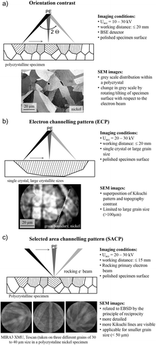
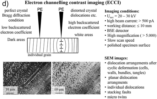
Figure (a) illustrates the conventional BSE orientation contrast where individual grains of a polycrystalline microstructure exhibit different grayscale levels in the BSE image due to the different crystallographic orientations of each grain with respect to the incident primary electron beam resulting in different backscattering contrasts. Tilting the specimen in the SEM leads to changes in the grayscale level of each individual grain due to the change of the crystal orientation with respect to the primary electron beam. In Figure (a), the different crystallographic orientations are symbolized by the different alignment of one set of lattice planes in the scanned grains.
ECPs as shown in Figure (b) allow the determination of the crystallographic orientation. Changes in the orientation relationships between primary electron beam and different lattice planes during the scanning procedure along the specimen surface result in Kikuchi lines forming ECPs, which are very similar to electron backscatter patterns. Best imaging conditions for ECP are small working distance and lower magnification leading to a large scanning angle 2Θ. However, the application of ECP is restricted to single crystals or polycrystalline material with a large grain size (>100 μm). In addition, the quality of ECPs is reduced by increasing dislocation density in the investigated material as reported by Stickler et al. [Citation8]. Furthermore, the ECPs are superimposed by the topography of the specimen surface and much care has to be taken on the surface preparation. Therefore, the ECP technique was rarely used.
The SACPs are quite similar to ECP. However, the SACPs are obtained by rocking the primary electron beam around a nearly stationary point on the specimen surface (see Figure (c)). Due to the different operating modes, more Kikuchi lines are visible and consequently more detailed crystallographic orientation information can be obtained. This makes SACPs favourable for the determination of orientations of smaller crystal sizes. However, special technical equipment at the SEM (SACP module) for rocking the primary electron beam was necessary in the past. Nowadays, however, in case of modern scanning electron microscopes (e.g. Tescan, MIRA3 [Citation9]; Zeiss, AURIGA [Citation10]) with enhanced electron path using a combination of objective lens and immersion lens, no additional rocking unit is necessary and SACPs can be obtained for polycrystalline materials with an average grain size of about 30–40 μm as shown in Figure (c) for polycrystalline nickel.
Special electron channelling contrast conditions can be used to image lattice defects in bulk materials – known as the ECCI technique shown in Figure (d). In principle, there is no fundamental difference to the above-described orientation contrast (see Figure (a)). However, the lattice distortions occurring from the presence of lattice defects lead to changes in the backscattering and channelling conditions depending on the deviation parameter (called e.g. ω in [Citation7] or s in [Citation10]) as nicely demonstrated by Zaefferer and Elhami [Citation7]. According to this description, the lattice defect contrast can occur either when the crystal is in channelling condition (bright defect contrast on a dark background) or in strong backscattering condition (dark defect contrast on a bright background). Figure (d) shows an ECC image of the dislocation arrangement after fatigue, where the dislocation dense regions (walls, veines) appear as constant bright contrast nearly independent on the grain orientation with respect to the primary electron beam. In addition, the ECCI image is shown in inverted contrast, which is then comparable to TEM studies.
3. Historical review on the development of the ECCI and its application to different types of materials
The TEM was, for a long time, a unique and excellent method for investigations on the nature of individual lattice defects (like dislocations, SFs, etc.) and their arrangements in different types of materials, and after different mechanical and thermal treatments [Citation5,11]. Already in 1967, Booker et al. [Citation2] stated that “it should be in principle possible to use the scanning electron microscope to detect dislocations by the direct examination of unetched crystal surfaces”. However, it took more than 20 years until the ECCI technique was successfully applied for investigations of individual lattice defects. This long period was necessary because HR-SEM equipped with field emission gun (FEG-SEM) had to be developed. The application of the electron channelling contrast applied in a scanning electron microscope for imaging lattice defects has opened a large new field in scanning electron microscopy. Table presents a historical review on the application of the electron channelling contrast for imaging individual dislocations and dislocation arrangements in different types of materials. The table includes also information about the used type of SEM, the applied ECC imaging parameters (as far as presented) as well as the main results of the investigations. The historical review is divided into three parts: (i) imaging of individual lattice defects, (ii) imaging of dislocation arrangements after fatigue and (iii) combination of ECCI with other SEM techniques.
Table 1. Review on investigations of dislocations and dislocation arrangements in different materials and after different mechanical loading applying the ECCI technique.
3.1. Imaging of individual lattice defects
Already five years after Coates and Booker discovered the ECPs; in 1972, Spencer et al. [Citation12] concluded from calculations using the dynamical diffraction theory that individual lattice defects like dislocations etc. may be visualized in thin foils under optimized conditions with a conventional scanning electron microscope (CSEM) equipped with a tungsten hairpin filament. Pitaval et al. [Citation13] and Morin et al. [Citation14] performed in 1977 and 1979, respectively, path-breaking experimental studies on individual dislocations by ECCI in SEM. At the beginning of the 1970s, these authors designed a cold field emission gun attached to SEM – Stereoscan MKII. With this instrument and a high-energy filter removing the low-energy BSEs, they were able to visualize individual dislocations in silicon (Si) single crystals operating at 40–50 kV acceleration voltage and tilt angles of 50 – 70°, the so-called high-tilt ECCI configuration. The authors stated also that the contrast of dislocations in electron channelling images depends on the g·b criterion as for TEM. Therefore, exact diffraction conditions are recommended, which were determined at this time using SACPs.
Since 1990, the number of investigations on individual dislocations by means of the ECCI technique was significantly increasing. Czernuszka et al. [Citation15] showed that it is possible to image and characterize individual dislocations in bulk specimens. The authors applied the ECCI technique using still the high-tilt configuration (tilt angle ~45°) in a high-resolution FEG-SEM in combination with a high-efficiency BSE detector yttrium-aluminium garnet film (YAG) without any energy filtering of the BSEs. The application of this method on different bulk materials (Si, Ni3Ga) allowed the visualization of individual dislocations with a contrast width of approximately 20 nm, which is comparable to the conventional TEM. Wilkinson et al. [Citation16] investigated clusters of misfit dislocations lying more than 1 μm below the surface at the interface between strained epitaxial Si–Ge layers on silicon substrates. However, at these depths, the resolution of ECC images is very low, thus individual dislocations cannot be resolved by this technique.
In the last decade, the group of Crimp and co-workers [Citation17–22] did a significant progress in the development of the ECCI technique to a robust routine alternative to TEM. In [Citation19,20], the experimental parameters and set-up necessary to carry out ECCI as a routine method are summarized. Whereas at the beginning of the 1990s, ECCI was applied at high-tilt configurations (~45° tilt of specimen with respect to the incident electron beam) with a side-mounted BSE detector, Simkin et al. [Citation19,20] recommended a low-tilt configuration (<10°) in combination with a pole piece-mounted standard 4-quadrant Si-diode backscatter detector. The authors showed that although the overall BSE signal is lower in the low-tilt configuration, the large collection angle (solid angle) of the pole piece-mounted detector offers best imaging conditions. Furthermore, the authors mentioned the numbers of advantages of ECCI investigations in comparison to TEM studies like (i) easy preparation of specimens since no electron transparent thin foil is necessary, (ii) large investigation area combined with good statistics and (iii) application to in situ studies on bulk materials.
Starting in 2009, the group of Pickard and co-workers [Citation23–26] adapted in the last years the ECCI to GaN and SiC films, in order to resolve burgers vector of individual threading dislocations propagating through the film thickness. It is stated by the authors that due to surface relaxations, the g·b criterion cannot be applied. Nevertheless, the spatial size effect of ECCI contrast features can be used to differentiate screw/mixed dislocations from edge threading dislocations.
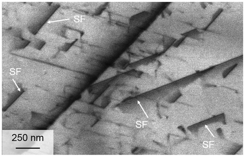
Quite recently in 2011, it was shown by Weidner et al. [Citation27,28] that lattice defects like SFs can be visualized by ECCI applied in a high-resolution FEG-SEM. The inverted ECCI micrograph in Figure shows examples for SFs in austenitic cast TRIP steels after tensile deformation (a) and after cyclic deformation (b). The resolution of the individual SFs in the HR-ECCI micrographs is comparable to that of conventional TEM [Citation5,11].
Figure 2. HR-ECCI micrographs (inverted) of individual SFs in austenitic cast TRIP steels G-X5CrMnNi16.6.6 (a) and G-X5CrMnNi16.6.3 (b) after tensile deformation up to 8% of elongation (a) and cyclic deformation at εa,t = 2.5 × 10⁻³ up to Nf = 130,508 cycles (b). [Citation27,28].
![Figure 2. HR-ECCI micrographs (inverted) of individual SFs in austenitic cast TRIP steels G-X5CrMnNi16.6.6 (a) and G-X5CrMnNi16.6.3 (b) after tensile deformation up to 8% of elongation (a) and cyclic deformation at εa,t = 2.5 × 10⁻³ up to Nf = 130,508 cycles (b). [Citation27,28].](/cms/asset/0095133a-7b43-4ecc-86b2-bdfcf6179bd2/tphm_a_1006296_f0002_b.gif)
3.2. Imaging of dislocation arrangements after fatigue
Since the beginning of the 1990s, numerous papers were published dealing with the investigation of dislocation arrangements in metallic materials after cyclic deformation. The group of Mughrabi and co-workers [Citation29–31] published the first papers on this subject. The authors give an overview on results of the first ECCI investigations on different types of materials after cyclic deformation like austenitic steel, copper and α-iron [Citation30]. A direct comparison of dislocation arrangements imaged both by applying conventional TEM as well as ECCI in a SEM with tungsten cathode and low-tilt ECCI configuration (tilt angle ≤10°) is presented. The authors demonstrated very well the usefulness of applying this technique in order to study dislocation arrangements after fatigue. They showed that it is possible to distinguish between dislocation walls, dislocation cells and subgrain structures. Furthermore, the authors highlighted that this relatively simple and efficient technique has a supplementary character to TEM investigations due to its advantages of simple specimen preparation and large field of view.
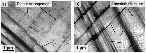
Few years later, Schwab et al. [Citation32] showed that dislocation glide localization phenomena like the “ladder-like” structure of dislocation walls in persistent slip bands (PSBs) occurring in nickel polycrystals after fatigue can be studied by the ECCI technique in a conventional SEM equipped with tungsten cathode and using the low-tilt ECCI configuration. Thus, it was possible to obtain statistically provided geometrical parameters (thickness of dislocation walls, thickness of dislocation free channels, etc.) of the dislocation arrangements in the composite of PSBs and matrix. In this context, Buque et al. [Citation33–35] investigated the influence of individual grain orientations as well as of the grain size on the occurring dislocation arrangements and the macroscopic heterogeneity of plastic deformation. The authors showed that the following four groups of dislocation arrangement patterns can be introduced and are sufficient in order to describe the high variety of dislocation configurations after cyclic deformation at different plastic strain amplitudes: (i) labyrinth structure, (ii) fragmented wall structure, (iii) bundle structure and (iv) patch structure. The ladder-like structure of dislocation walls correlated with PSBs occurs mostly in the bundle-type structure, but can be observed also in all other dislocation patterns. In [Citation35], it is shown that increasing grain size leads to a fragmentation of the grain orientation-dependent dislocation arrangement into parts with different mesoscopic parameters.
Recently, Zhang et al. [Citation36] as well as Li et al. [Citation37] performed intensive studies concerning the formation mechanisms of dislocation arrangements in fcc single crystals [Citation37] as well as in bi-crystals concerning the influence of special grain boundaries on cyclic deformation and fatigue damage [Citation36].
The experimental results on fcc metals with planar dislocation glide behaviour offer a far less clear picture. Although there is a clear evidence of cyclic slip localization also in these materials, no systematic studies on the dislocation arrangements in these materials are available. Until now, dislocation arrangements have been studied mainly using TEM e.g. in the case of single crystals of Cu–Zn [Citation38] and Cu–Al [Citation39] alloys. Buchinger et al. [Citation40] found dislocation arrangements corresponding to localization of the cyclic plastic strain – so-called “persistent” Lüders bands. Kaneko et al. [Citation41] applied ECCI to an austenitic Fe-19% Ni–11% Cr steel cyclically deformed at different stress levels to half of the fatigue life. The authors revealed slip localizations in bands with a dislocation arrangement in the surface grains (SGs), which are more or less reminiscent to the ladder-like structure as well as vein structures in materials with pronounced cross slip behaviour like nickel or copper. It was also shown that these band structures are persistent.
Quite recently, for bcc materials, Shih et al. [Citation42] investigated the fatigue behaviour of interstitial free steel (IF) at different total strain amplitudes and correlated the occurrence of secondary hardening for medium strain amplitudes with the formation of small dislocation cells.
3.3. Combination of ECCI with other SEM techniques
Up to now, defined diffraction conditions based on ECP [Citation14,22,43,44] or SACP [Citation45,46] were necessary for the investigation of individual dislocations by ECCI. However, these methods are limited by necessary large grain sizes (ECP) or instrumental conditions (SACP). Quite recently, a novel set-up for ECCI under controlled diffraction conditions was introduced by Gutierrez-Urrutia et al. [Citation48] – so-called cECCI (controlled ECCI). This set-up uses the high spatial resolution (about 30 nm [Citation49]) of EBSD measurements for the determination of the crystal orientation in the area which is interesting for ECCI of dislocations or twins. Computer software [Citation50] is used to calculate diffraction patterns of studied ECCI areas. Best diffraction conditions for the selected ECCI area were then obtained by slight tilting and rotating of the specimen in order to set up defined diffraction conditions. In [Citation51,52], the authors present results of combined EBSD and ECCI investigations of the dislocation and micro twin evolution during tensile deformation of a Fe–Mn–C Twinning Induced Plasticity (TWIP) steel. Furthermore, the novel EBSD-based set-up for ECCI is used to determine the dislocation density in a tensile deformed Fe–Si alloy [Citation53,54]. The dislocation densities measured under different diffraction conditions (two- and three-beam conditions) represent average dislocation densities, which are comparable to such obtained by standard bright-field TEM. Gutierrez-Urrutia et al. [Citation55,56] demonstrated on different examples that the cECCI coupled with EBSD opens the field for a quantitative description of deformation structures using SEM instead of TEM. Among an interpretation of the channelling contrast resulting from lattice defects using two-beam Bloch wave approach, they showed that quantitative values for dislocation densities and nanotwins can be obtained using the ECCI technique. Quite recently, Zaefferer et al. [Citation7] published a fundamental paper according to cECCI in terms of theoretical approaches and practical aspects together with some case studies. Moreover, Mansour et al. [Citation10] published a second method of controlled ECCI technique – so-called accurate ECCI (aECCI). Mansour et al. favours the coupling of high angular and spatial resolution SACP (HR-SACP) and ECCI for the controlled set-up of crystals for perfect imaging conditions for imaging individual lattice defects. The authors argue that an alignment of the crystal orientation is necessary to achieve an optimum contrast. However, to set up a crystallographic orientation at an exact deviation parameter seems to be difficult. The authors demonstrated nicely on a 2% Si-IF steel that the collection of HR-SACP in combination with simulated EBSD pattern opens a new gate to perform “TEM style contrast analysis of dislocations from even relatively fine grained polycrystals” [Citation10].
3.4. Summary of historical review
Thus, the historical overview shows that the ECCI technique has been developed during the last about 50 years to a powerful technique for the investigation of individual lattice defects as well as dislocation arrangements after different mechanical treatments and in different materials. This great step forward is the result of a significant progress in the development of HR-SEMs. In addition, the change from the high-tilt to the low-tilt condition for ECCI – proposed for the first time by Crimp and co-workers – made the application of ECCI in a SEM to bulk materials to a reliable technique for the analysis of deformation structures similar to TEM. Finally, both the cECCI [Citation7] using EBSD as well as the aECCI [Citation10] using SACP to set up the crystallites in proper imaging conditions will open a gate to go ahead from a more or less qualitative description of defect arrangements to a quantitative characterization.
Using high-resolution field emission scanning electron microscopes (HR-FEG-SEM), it is possible to visualize lattice defects like SFs or individual dislocations in bulk materials with a comparable resolution as obtained for conventional TEM on electron transparent foils. Nowadays, ECCI micrographs taken in HR-FEG-SEM can be called HR-ECCI.
In the following, the authors will summarize some case studies of the application of the HR-ECCI technique to different materials mainly after cyclic deformation, but also after monotonic loading. It is not in the focus of the following sections to give a closed description of the fatigue or monotonic loading behaviour of the chosen materials or to describe the influence of the composition of the materials on the adaptability of the ECCI technique.
4. High-resolution ECCI and the investigation of defect arrangements after monotonic or cyclic deformation
In the following, the application of the ECCI technique using the low-tilt ECCI configuration in different types of scanning electron microscopes is presented. It is demonstrated that it is possible to obtain HR-ECCI micrographs showing individual lattice defects like SFs and individual dislocations using high-resolution FEG-SEM. Nevertheless, excellent ECCI micrographs showing dislocation arrangements like wall, bundle or labyrinth structures after cyclic loading can be obtained even in conventional SEMs equipped with tungsten cathode. Furthermore, the following section is also demonstrating that HR-ECCI micrographs can be obtained for different types of materials and different grain sizes ranging from large grain size of 500 μm (cast steel) down to less than 2 μm (γ-TiAl). In all presented examples, the ECCI investigations were accompanied by EBSD measurements. However, for detailed information on results of these EBSD measurements, the reader is kindly asked to refer to respective refs.
4.1. Experimental set-up
The ECCI investigations were performed in four different types of scanning electron microscopes, which were equipped either with a tungsten cathode or with a field emission gun.
The SEM with the tungsten cathode (DMS 962, ZEISS) was equipped with a four-quadrant retractable backscatter detector from KE Developments (UK). ECCI technique was performed in low-tilt condition at an acceleration voltage of 20 kV, an aperture of 70 μm and at working distances of about 10–11 mm. By this, dislocation arrangements after cyclic deformation of Ni polycrystals were imaged. This material is a representative candidate for pronounced cross slip behaviour and for the development of arrangements of dislocations in wall, bundle, veins, cell and labyrinth structures or the well-known ladder-like structure of PSBs in fatigue.
As SEMs with a field emission gun, an ULTRA55 (ZEISS), a LEO 1540 (ZEISS) and a MIRA 3 XMU (TESCAN) were used equipped with four-quadrant BSE-detectors, a pole piece-mounted detector in case of the ULTRA55 and retractable detectors in the LEO 1540 and the MIRA 3 XMU SEMs. Working distances down to 3 mm were possible in ULTRA55, about 5 mm in LEO 1540 and 8 mm in MIRA 3 XMU. For all three microscopes, the used acceleration voltage was 20 kV. Using the ULTRA55 and the LEO 1540 with an electron column working after the GEMINI principle, an aperture of 120 μm and a so-called high-current mode leading to about 20 nA beam current was applied. In the MIRA3 XMU, a unique real time “in-flight beam tracing™” technology working with a single aperture of 10 μm and continuous adjustable beam current up to 100 nA is applied; the effective probe current and also the resulting diameter of the electron beam on the specimen surface are permanently available.
ECPs for crystallites of a grain size of less than 50 μm can be obtained at lower working distances and magnifications using a combination of objective and immersion lens in the MIRA3 XMU.
EBSD systems using the Channel5 software (hkl-Oxford) and OIM software (TSL) were available for the data acquisition and analysis on the DSM 962, LEO 1530, Ultra55 and the MIRA3 XMU, respectively.
4.2. Materials and specimen preparation
Specimens at different stages of plastic deformation were analysed by ECCI or combined ECCI/EBSD investigations. Table gives a summary of the investigated deformation states. Hereby, the table is divided into fatigue tests and tensile tests. Furthermore, the investigated materials are grouped to materials showing (i) wavy glide behaviour, (ii) planar glide behaviour or (iii) a transition from planar and to wavy glide behaviour depending on the applied cyclic deformation amplitude. Most mechanical tests were performed on servo hydraulic testing machines (MTS, Instron). Special testing parameters for individual specimens can be found in given references.
Table 2. Materials and mechanical test parameters of specimens investigated by ECCI/EBSD.
In addition, Table gives information whether the investigations were performed on surface grains (SGs) or in the bulk material (BG). In case of investigations on SGs, the specimens were prepared by grinding and mechanical polishing followed by electrolytic polishing prior to the mechanical tests. After the mechanical tests, occurring slip markings at the specimen surface were removed either by electrolytic or vibration polishing. In case of investigations on bulk grains, the gauge length of the specimens was sectioned parallel to the loading axis followed by grinding and mechanical polishing.
Careful surface finish is strictly required for ECCI investigations, since ECCI is applied in order to investigate individual dislocations or dislocation arrangements near the specimen surface. Therefore, it is necessary that the surface is free of preparation damage layer or other artefacts. The best ways to guarantee the necessary surface quality are electrolytic polishing or vibration polishing. For electrolytic polishing, the typical material specific electrolytes and polishing parameters were used. Vibration polishing was performed by the vibratory polisher VibroMet® 2 (Buehler). It removes minor deformation remaining after mechanical preparation and yields high-quality polished surfaces. It is applicable for a wide range of materials and is the preferred method for multiphase materials and composite materials. It is often used as an excellent EBSD polishing technique. A superior quality result and exceptional flatness of the specimen surface is obtained by a horizontal motion of 7200 cycles per minute producing very effective polishing action. Vibration polishing produces less deformation, flatter surfaces and reduces edge rounding. It also yields a stress-free surface without problems associated with e.g. electro-polishing or ion milling. In the present studies, vibration polishing was performed for 24 h using a SiO2 suspension followed by a final careful cleaning procedure.
However, contamination effects have a significant negative influence on the quality of ECCI micrographs. Therefore, it is necessary to keep the contamination level during the ECCI investigations at a minimum. In order to minimize contamination, it is useful to avoid any resin or carbon tapes. In case of previously performed EBSD measurements, which results very often in a contamination layer, it is recommended to remove this layer by plasma cleaning.
4.3. Individual lattice defects after tensile and cyclic deformation
Pitaval et al. [Citation11] and Morin et al. [Citation12] demonstrated already at the end of the 70’s that it is possible to visualize individual lattice defects like dislocations or SFs by the application of the ECCI technique in a scanning electron microscope. At that time, a so-called high-tilt ECCI configuration (about 45° tilt of the specimen) was used in one of the first SEMs with a cold field emission gun and an acceleration voltage of about 50 kV. They obtained as an outstanding result for that time period first images of individual dislocations in a silicon single crystal under different diffraction conditions with an acceptable resolution. Nowadays, more than 30 years later, the development of high-resolution FEG-SEMs yields significant improvement in the resolution of SEM images comparable to conventional TEM bright field.
4.3.1. Observation of SFs by HR-ECCI
Using high-resolution FEG-SEMs in combination with the ECCI technique allows to visualize planar lattice defects like SFs with a resolution comparable to conventional TEM. In materials with a low stacking fault energy (SFE), regular dislocations shows a high tendency to dissociate into Shockley partial dislocations generating two-dimensional SFs in between the partial dislocations. Due to external stress, the two partial dislocations move in opposite directions leading to largely extended SFs. Thus, the SF distance depends on the applied stress [Citation70]. Consequently, plastic deformation leads to a high density of SFs, which are in some materials grouped together in deformation bands. The density of SFs in these deformation bands may get so high, that individual SFs cannot be resolved by electron microscopy. The investigation of such bands in an austenitic steel by EBSD measurements revealed a hexagonal lattice structure in these regions, which is clearly caused by the high density of SFs [Citation27,71]. The deformation bands with the hexagonal lattice structure correspond always to slip systems with a high Schmid factor. However, in between these bands or along slip systems with lower Schmid factor, individual SFs become visible applying the ECCI technique.
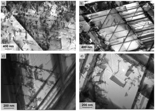
Figure shows two examples of HR-ECCI micrographs visualizing individual SFs in metastable high-alloy austenitic cast steel after uniaxial tensile (a) and cyclic (b) deformation, respectively. The investigated steel exhibits a quite low SFE of about 17 kJ/mol [Citation72,73] and, therefore, a high tendency to form SFs. In both micrographs, deformation bands on different activated slip systems as well as individual SFs are clearly visible. The SFs show the typical fringe contrast which is well known from TEM images [Citation5]. Similar to the thickness contrast in TEM [Citation5], the fringes result from oscillations of the intensity of BSEs on a SF [Citation55]. Figure (c) and (d) shows additional transmission SEM (t-SEM) images taken on a TEM foil of the same material as shown in Figure (a) using a transmission electron detector in a SEM (MIRA3 XMU) using an acceleration voltage of 30 kV and a low working distance (3 mm). Deformation bands consisting of overlapping SFs as well as individual SFs are clearly visible. Thus, the application of modern FEG-SEM also for transmission microscopy is well demonstrated. In the present case, the comparison of inverted ECCI and t-SEM verifies that the planar defects are really SFs.
Figure 3. Inverted ECCI micrographs on bulk specimens (a,b) and t-SEM images on a TEM foil (c,d) of high-alloy TRIP steels showing individual SFs. (a) G-X5CrMnNi16.6.6 after tensile deformation to 8% of elongation. (b) G-X5CrMnNi16.6.3 after cyclic deformation with a total strain amplitude εa,t = 2.5 × 10⁻³ up to failure (Nf = 130,508).(c,d) G-X5CrMnNi16.6.6 after tensile deformation up to 8% of elongation. TE-detector was used in a FEG-SEM at 30 kV acceleration voltage. In (a,b) loading axis is horizontal.
The calculated extinction distance for a {1 1 1} diffraction vector at 20 kV in f.c.c iron, which is 14 nm is in good agreement with results recently reported by Gutierrez-Urrutia et al. [Citation55] and Zaefferer and Elhami [Citation7]. The analysis of the crystallographic orientation obtained from additional EBSD measurements revealed that the SFs visible in Figure (b) lie on (1 1 1) planes, which are inclined at an angle of 22° with respect to the specimen surface. At least two full sets of extinction fringes are clearly visible. The measured thickness of the fringe contrast of the SF is about 15 nm (see Figure (b)). Taking into account the inclination of the SF with respect to the surface, the information depth of SF contrast shown in Figures (a), (b) and is about 50–80 nm. However, for SFs lying in a depth less than the extinction distance, no full period of fringe contrast can be observed. Thus, SFs appear then “only” as a shadow in the bright contrast of the rest of the grain as indicated by white arrows in Figure .
Figure 4. Inverted ECCI micrographs of a high-alloy TRIP steel (G-X5CrMnNi16.6.6) after tensile deformation to 8% of elongation with indicated {111} planes (a) and measured width of contrast fringes of individual SF (b). The insert in (a) demonstrates the grain orientation obtained by EBSD. (b) is a part of (a) at higher magnification).
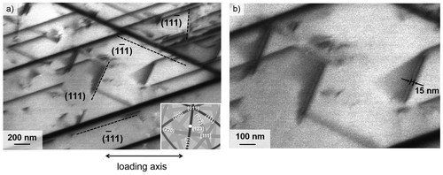
Figure 5. Inverted ECCI micrograph of a high-alloy TRIP steel (G-X5CrMnNi16.6.6) after tensile deformation at room temperature up to 8% of elongation showing individual SFs along two different {1 1 1} planes without full period of fringe contrast.
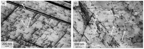
Nevertheless, among SFs also regular dislocations participate on the deformation process, as well. Therefore, individual dislocations can be observed after monotonic tensile deformation too. However, due to the locally introduced high lattice distortion, the visualization of individual dislocations is more difficult and limited to lower strain levels. Figure (a) shows a mixture of deformation bands, individual SFs and individual regular dislocations in a G-X5CrMnNi 16.7.6 steel specimen tensile deformed up to a strain of ε = 8%. Figure (b) shows the formation of an individual deformation band by several SFs along the primary slip plane together with individual regular dislocations (marked by white arrows) in the austenitic matrix. Both mechanisms – the movement of partial dislocations forming SFs as well as the regular dislocation glide – are mainly active at lower strain levels (in this case 8%) followed by the formation of deformation induced α’-martensite at larger strains, as demonstrated by Vinogradov et al. [Citation74] using acoustic emission measurements in combination with advanced method of pattern recognition and cluster analysis.
Figure 6. Inverted ECCI micrographs of a high-alloy TRIP steel (G-X5CrMnNi16.6.6) after tensile deformation at room temperature up to 8% of elongation. (a) Mixture of deformation bands, individual SFs and regular dislocations. (b) Development of a new deformation band by grouping of several individual SFs along the same slip plane and regular dislocations in the austenitic matrix.
4.3.2. Observation of individual dislocations by HR-ECCI
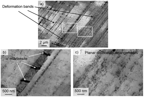
HR-ECCI allows the observation of individual dislocations in the microstructure of different deformed metallic materials (see also planar dislocation arrangements in Section 4.4). Figure shows the dislocation arrangement for a γ-TiAl alloy TNB-V5 after thermo-mechanical fatigue. The microstructure of this material consists of duplex structure of globular γ-TiAl (tetragonal phase) and lamellar colonies of alternating γ-TiAl lamellas and α2-Ti3Al lamellas (hexagonal phase). Intensive TEM investigations of microstructures after cyclic loading up to high temperatures (973 K) revealed that the deformation behaviour of two-phase γ-TiAl alloys is determined by the easy activation of regular dislocation glide and mechanical twinning [Citation75]. Furthermore, Henaff and Gloanec [Citation76] observed recovery and climb processes as well as remnant dislocation loops in an ordinary dislocation arrangement after LCF tests at 723 K. In comparison to TEM investigations, ECCI studies on bulk specimens allow to investigate the dislocation arrangements with a reasonable good statistic without demanding and time consuming preparation of thin foils. Details on the investigated material and the thermo-mechanical fatigue tests are presented in [Citation77,78]. The inverted ECC images in Figure clearly reveal that the deformation microstructure can be visualized within the γ-TiAl phase both in globular grains (a,b) with a mean grain size of few micrometres (2–4 μm) as well as in lamellar regions (c,d) with an interlamellar distance below 1 μm. Both, in the globular as well as in the lamellar γ-TiAl phase, individual dislocations and dislocation tangles are visible. The individual dislocations are largely extended screw dislocations, which are pinned in some case (black dots). In addition, micro twins (arrows) have been formed.
Figure 7. Inverted ECC images of the dislocation arrangements in γ-TiAl TNB-V5 alloy after thermo-mechanical fatigue in the temperature range of 673 K < T < 923 K with a mechanical strain amplitude of εa,mech = 5.75 × 10⁻³. (a,b) Globular γ-TiAl grains. (c,d) Lamellar regions. (after [Citation65]).
![Figure 7. Inverted ECC images of the dislocation arrangements in γ-TiAl TNB-V5 alloy after thermo-mechanical fatigue in the temperature range of 673 K < T < 923 K with a mechanical strain amplitude of εa,mech = 5.75 × 10⁻³. (a,b) Globular γ-TiAl grains. (c,d) Lamellar regions. (after [Citation65]).](/cms/asset/bb134379-4fec-46b9-b9d7-597023d3c091/tphm_a_1006296_f0007_b.gif)
A comparison of the ECCI technique with complementary, conventional TEM studies performed on TEM foils of the deformed material are shown in Figure as verification of the results obtained in the ECCI investigations. Figure (a) shows the inverted HR-ECCI micrograph of a globular γ-TiAl grain with elongated screw dislocations as well as dislocation tangles. The screw dislocations are pinned and in some cases, remnant dislocation loops are visible. In comparison, Figure (b) shows the dislocation arrangement in a globular γ-TiAl grain as well, but taken using classical TEM at 200 kV [Citation65]. Elongated screw dislocations are visible as well. It is vividly seen, that the defect types and/or arrangements visualized by application of the ECCI technique are in resolution comparable to those obtained from TEM investigations. The image width of individual dislocations visualized by ECCI is about 15 nm, which is similar to conventional TEM. Furthermore, it becomes evident that the investigation of dislocation and/or defect arrangements using the ECCI technique on a bulk specimen can be performed with a reasonably good resolution as well as good statistics. By applying EBSD measurements before or after the ECCI investigations [Citation65], it is even possible to investigate the influence of crystallographic orientation on special dislocation arrangements within a reasonable time frame.
Figure 8. Comparison between inverted ECCI (a) and convential TEM (b) micrograph of the dislcation arrangement in a globular γ-TiAl grain. [after 65]. Details see Figure .
![Figure 8. Comparison between inverted ECCI (a) and convential TEM (b) micrograph of the dislcation arrangement in a globular γ-TiAl grain. [after 65]. Details see Figure 7.](/cms/asset/0eb3ee54-1cd8-4a64-a128-f1378d3dd16c/tphm_a_1006296_f0008_b.gif)
4.4. Planar dislocation arrangements after fatigue
The dislocation arrangement in metallic materials due to cyclic deformation is among other parameters strongly affected by the character of slip – planar slip and cross slip. The planarity of slip in metals and alloys depends on the SFE of dislocations as well as on the short-range order (SRO). Depending on the SFE, fcc metals and alloys can be divided into two groups: materials with pronounced cross slip behaviour (high SFE) and planar glide materials (low SFE) [Citation79–81]. The cross slip of dislocations is easier for higher SFE which results in wavy slip. However, interstitials like nitrogen or carbon as alloying elements for instance in austenitic stainless steels inhibit cross slip of dislocations and promote planar slip. Takemoto et al. [Citation82] showed that the planar distribution of dislocations is attributed to a SRO zone. For a recent review on wavy-to-planar-slip transition, see also [Citation83].
4.4.1. Planar dislocation arrangement at early state of fatigue
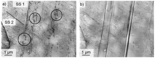
The austenitic stainless steel 316L with a low SFE (37 mJ/m²) exhibits pronounced planar glide behaviour. Thus, dislocations are arranged along activated slip planes, and cross slip is hindered due to the dissociation of regular dislocations into Shockley partial dislocations. Experimental investigations of the cyclic deformation of this type of fcc metals with planar slip behaviour offer a far less clear picture than materials with a pronounced cross slip behaviour like copper or nickel. In the path, dislocation arrangements have been studied mainly using TEM or in some cases by ECCI investigations at half of fatigue life or in the vicinity of cracks [Citation41]. However, a systematic study of the development of dislocation arrangements within slip localizations and individual grains with respect to their crystallographic orientation is still missing for planar glide materials. Therefore, studies on dislocation arrangements in an austenitic stainless steel (AISI 316L) were performed at an early stage of cyclic deformation [Citation68]. In contrast to PSBs in nickel (cf. [Citation84,85]) or in copper (cf. [Citation86,87]), the arrangement of dislocations is not in such a clear “ladder-like” structure. An example for the dislocation arrangement at an early stage of cyclic deformation of a 316L specimen is shown in Figure . Already, after 1000 cycles, first slip markings occur on the specimen surface. An intermediate state between planar and wavy dislocation arrangement along two different activated slip systems (SS1, SS2) at this early stage of fatigue is shown in Figure (a). Whereas, SS2 shows more or less a planar-like dislocation arrangement, first arrangement of dislocations in wall-type structures occurs along SS1 (marked by circles in Figure (a)). This dislocation arrangement belongs to the slip markings observed at the surface. Continuing in cyclic deformation of the specimen for additional 500 cycles demonstrates the persistency of these slip bands (along SS1) because exactly at the same areas of the first localized dislocation arrangements, the slip markings occur again at the specimen surface (see. Figure (b)).
Figure 9. Inverted ECCI micrographs of an individual grain in polycrystalline austenitic stainless steel AISI 316L after cyclic deformation with εa,p = 1 × 10⁻³ up to 1000 cycles showing dislocation arrangement along two different slip systems (a). (b) Surface slip markings after 500 additional cycles. Loading axis is horizontal. (FEG-SEM, ZEISS Ultra 55).
4.4.2. Planar dislocation arrangement and martensitic phase transformation
At room temperature, the austenitic stainless steel AISI 316L contains of a stable austenitic phase without martensitic phase transformation from the austenite (fcc) into the α’-martensite (bcc) during deformation. The stability of the austenite can be characterized among others by the martensitic start temperature Ms and the Md30 temperature, which represents the lowest temperature where 50% of deformation-induced α’-martensite is formed at a true strain of 30%. The calculated Ms and Md30 temperatures for AISI 316L are 77 and 255 K, respectively, indicating a high austenite stability. In Ref. [Citation88], experimental studies on the stability of austenite in 316L steel during cyclic deformation at room and low temperatures were performed. These investigations showed that the steel AISI 316L exhibits a very high stability during cyclic deformation at room temperature even at high plastic strain amplitudes (εa,p = 9.5 × 10⁻³) and thus, no deformation-induced α’-martensite was detected.
However, formation of deformation-induced martensite was found to a small extent after cyclic loading with high plastic strain amplitude at low temperature of 110 K. Figure shows inverted ECCI images of an individual austenitic grain exhibiting a planar dislocation arrangement in two activated slip systems (Figure (a)). Lenticular islands of α’-martensite (white arrows) were found at intersection points of crossing deformation bands (Figure (b)). Unfortunately, in the present case, these islands are too small for a phase identification with EBSD. However, in other grains, where the islands were much larger, they were identified as α’-martensite via EBSD [Citation89]. This is in very good agreement with [Citation90] showing a direct phase transition from the austenite (fcc) to martensite (bcc). Figure (c) shows the planar arrangement of individual dislocations along two different slip systems.
Figure 10. Inverted ECC images of the planar dislocation arrangement in an individual austenitic grain of the steel AISI 316L cyclically deformed at 110 K with a plastic strain amplitude of εa,p = 9.5 × 10⁻³. (a) Deformation bands on two different slip systems. (b) Islands of α’-martensite. (c) Planar arrangements of individual dislocations in two different slip systems without martensitic phase transformation. (b) and (c) are details of (a). Loading axis is horizontal. (FEG-SEM, ZEISS LEO 1530).
4.4.3. Transition from planar glide to cross slip behaviour
It is known from the literature [Citation86,91] that the dislocation arrangements in fcc metals and alloys strongly depend on the plastic strain amplitude and SFE resulting partly in a transition from planar to cross slip behaviour. A well-known example for this behaviour is the austenitic stainless steel AISI 316L. At low plastic strain amplitudes, this steel exhibits pronounced planar glide behaviour as already described in Section 4.4.1. At higher strain amplitudes or at low strain amplitudes in the vicinity of stress concentrations like crack tips the formation of cell, wall or labyrinth structures were observed [Citation38].
A comparable behaviour was observed also for a metastable high-alloy austenitic steel. Figure shows dislocation arrangements in a high-alloy austenitic cast TWIP steel (G-X5CrMnNi16.7.9) cyclically deformed at two different total strain amplitudes up to failure (Nf). Characteristic microstructural feature of this type of metastable austenitic stainless steel is the formation of deformation bands (see arrows) consisting of numerous micro twins. Very locally only, the formation of α’-martensite at the intersection points of those bands can occur. For low strain amplitudes, Figure (a) shows in addition to these deformation bands a pronounced planar dislocation arrangement along two slip planes. In contrast, at higher deformation amplitudes, a pronounced labyrinth structure is observed (see Figure (b)).
Figure 11. Inverted ECC images of the dislocation arrangement in cyclically deformed high-alloy TRIP steels G-X5CrMnNi16.7.8. (a) εa,t = 6 × 10⁻³. (b) εa,t = 1.2 × 10⁻². Loading axis is horizontal. (FEG-SEM, ZEISS LEO 1530).
4.5. ECCI and the slip activity of PSBs
Pure polycrystalline nickel (99.9%) with a high SFE (180 [Citation92]–300 [Citation93] mJ/m²) shows pronounced cross slip of dislocations resulting in wavy glide behaviour. Due to the activation of cross slip, the arrangement of dislocations is characterized by the formation of dislocation walls and cells. During cyclic deformation, slip localization occurs in form of so-called PSBs [Citation94], which are characterized by the well-known “ladder-like” structure of the arrangement of dislocation dense walls [Citation95,96]. PSBs emerging at the specimen surface cause so-called persistent slip markings (PSMs) forming a pronounced surface relief composed of extrusions and intrusions [Citation97,98], which are preferred locations for crack initiation. Two different approaches were pursued in the literature investigating the influence of PSBs/PSMs on the crack initiation and propagation [Citation99,100]: (i) development of extrusion/intrusion profile in dependence on the number of cycles [Citation101] and (ii) determination of the half-cycle slip activity of PSB. Schwab et al. [Citation84] as well as Hollmann [Citation85] performed half-cycle experiments on nickel single crystals at room temperature [Citation81] and low temperatures [Citation85] in order to study the slip activity of PSBs. Weidner et al. [Citation62–64] adopted this technique for the investigation on the cyclic slip activity of PSBs in polycrystalline nickel. The ECCI technique was complemented by EBSD and atomic force microscopy (AFM) for studying the half-cycle slip activity [Citation84,85]. Polycrystalline nickel with mean grain size of about 70 μm was cyclically deformed with low plastic strain amplitude up to 7500 cycles and 30,000 cycles, which correspond to 0.15 and 0.6 Nf, respectively [Citation62]. The ECCI micrographs in Figure illustrate the appearance of typical dislocation arrangements with PSBs in a matrix of dislocation veins and bundles at 7500 cylces (a,b) and 30,000 cycles (c,d), respectively. At lower number of cycles, the majority of PSBs can be described as individual PSBs with a thickness dPSB < 5 μm. At higher number of cycles, the individual PSBs tend to develop into so-called macro-PSB with 5 < dPSB < 50 μm. The “ladder-like” arrangement of dislocation walls is then turned into a pronounced cell structure.
Figure 12. Inverted ECC imaging of dislocation arrangements in polycrystalline nickel after cyclic deformation with εa,p = 5 × 10⁻⁴ up to 7500 cycles (a,b) and 30,000 cycles (c,d), respectively. Loading axis is horizontal. (FEG-SEM, Zeiss Ultra 55).
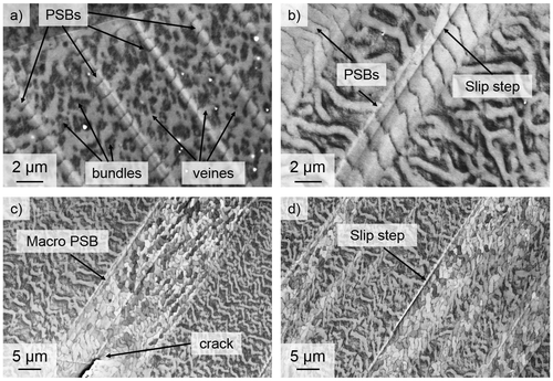
Imaging of PSBs by ECCI is mainly useful for the determination of parameters like dislocation wall thickness and channel width [Citation102] or the dependence of the PSB formation on the crystallographic orientation and/or grain size [Citation103] due to the good statistics, which can be achieved by this method. Another aspect for which the ECC imaging can be used is the investigation of the activation of cyclic slip within the PSBs [Citation62]. For such investigations, the specimens were pre-deformed to a certain number of cycles (e.g. 0.15 and 0.6 Nf in Figure ) followed by removal of the surface slip markings and subsequent half-cycle (hc) deformation in tension. Imaging the dislocation arrangements by ECCI revealed that places where cyclic slip is activated during a hc deformation and appears as slip steps at the surface. These slip steps occur as dark lines in the ECCI images (see Figure (b) and (d)). It becomes evident that neither at 7500 cycles nor at 30,000 cycles, the whole PSB is active. It is vividly seen that only a small part is active and that no preferred place for the activation of cyclic slip exists in an already well-developed PSB. The visibility of activation of cyclic slip during hc deformation in ECC images allows a pre-screening of grains, which can be then later subjected to detailed measurements of the slip step height and width using AFM [Citation62]. Knowing the crystallographic orientations from EBSD measurements, the local shear strain amplitude can be calculated for individual slip steps [Citation64].
Starting with this point, the ECC micrographs can be used also for the investigation of the reversibility or irreversibility of cyclic slip in individual PSBs [Citation104] during one full cycle (hc in tension plus hc in compression). The terms of hc and full-cycle (fc) deformation as well as total reversibility, partial reversibility and total irreversibility become evident from Figure . Figure (a)–(c) explains schematically the applied cyclic pre-deformation up to 0.6 Nf, the hc in tension as well as the fc in terms of the plastic strain hysteresis loops with starting and end point of loading cycles. Figure (d)–(g) shows the different cyclic slip reversibility / irreversibility behaviour of PSBs.
Figure 13. (colour online) Description of the cyclic pre-deformation up to 0.6 Nf (a), the half-cycle deformation in tension (b) and the full-cycle loading (c) in terms of plastic strain hysteresis loops with indicated start/stop points. (d-g) Definition of slip irreversibility during full-cycle loading (black – origin, red – half cycle, blue – full cycle). Surface displacements u and thickness D of the part of PSB activated during the hc or fc loading. (d) Slip step after hc loading in tension. (e) Full reversibility plus an additional new fc loading slip step (case A). (f) Partial irreversibility (case B). (g) Total irreversibility with additional full-cycle loading slip step (case C).
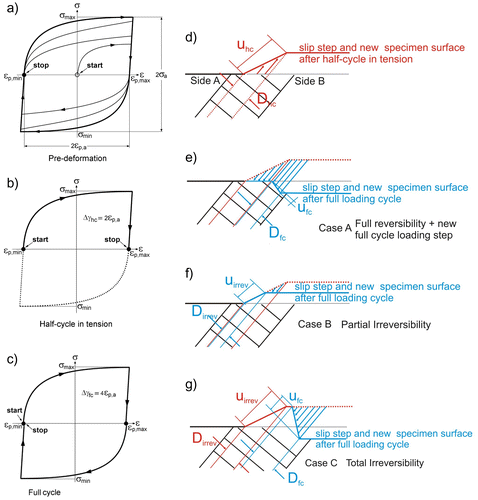
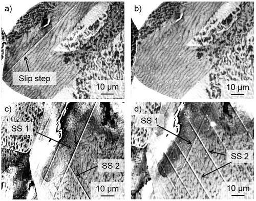
Here, the parameter u describes the surface displacement measured along the Burgers vector b of the activated slip system and D the thickness of the part of PSB, which is active during the hc loading. It becomes obvious that, depending on the observed PSB, four different cases can be observed: (i) full reversibility (case 0) (not shown in Figure ), (ii) full reversibility plus an additional new fc loading slip step (case A), (iii) partial irreversibility (case B) and (iv) total irreversibility with additional full-cycle loading slip step (case C). These four different cases can be observed directly from ECC images due to the change of contrast of slip steps formed within the microstructure after fatigue, mainly in PSBs. Of course, this is only a qualitative interpretation and has to be verified by detailed profile measurements using AFM, for more detail see [Citation64]. Results of the experimental determination of the cyclic slip irreversibility factor on basis of these findings were published in Ref. [Citation104]. This example demonstrates that the ECCI technique is very useful for a pre-screening due to the large field of view and, therefore, good statistics for selection of interesting PSBs and/or grains. Figure shows an example for the activation of cyclic slip within two different grains after hc loading (a,c) and fc loading (b,d). The different behaviours of localized cyclic slip in the two grains become evident. Grain 1 (a,b) shows complete reversibility of cyclic slip. The slip step formed during the hc in tension (a) disappears completely during the fc loading (b). The situation in grain two is more complex. During the hc in tension, cyclic slip is activated on two different slip systems (SS 1 and SS 2) on few parts of the grain only (c). The fc loading reveals three different processes: (i) activation of cyclic slip on new places related to slip system SS 2, (ii) partial reversibility of cyclic slip in slip system SS 1 (case B) and (iii) full reversibility on slip system SS 2 plus additional cyclic slip during the fc loading. The ECCI technique is in this case again valuable for pre-screening of slip activities in several grains.
Figure 14. Inverted ECC imaging of the cyclic slip reversibility / irreversibility on polycrystalline nickel after cyclic pre-deformation up to 30,000 cycles followed by half-cycle deformation in tension (a,c) and additional half-cycle deformation in compression (b,d). Loading axis is horizontal. (CSEM, Zeiss DSM 960).
5. Summary
The present paper shows that the application of the high-resolution electron channelling contrast-imaging technique is a powerful tool to investigate both dislocation arrangements and individual lattice defects like SFs, dislocations or micro twins in various metallic materials after different mechanical loading conditions using a large variety of scanning electron microscopes. The resolution of the ECCI micrographs of individual lattice defects is comparable with the image resolution of conventional TEM micrographs. Moreover, the results demonstrated very well that the ECCI technique is a powerful method for characterization of the microstructure after deformation in combination with other techniques like EBSD or AFM. However, the most important requirements for HR-ECCI are, in addition to the use of a HR-FEG-SEM, an excellent specimen surface preparation by electro or vibration polishing as well as an experienced and patient operator.
Acknowledgements
The authors thank Prof. W. Skrotzki and Dr E. Hieck-mann for supporting with SEM investigations on the Ultra55 at the Institutes of Structural Physics and Semiconductor Physics of Technische Universität Dresden. Prof. D. Rafaja is grateful acknowledged for providing the SEM LEO 1530 at the Institute of Materials Science of Technische Universität Bergakademie Freiberg. Dr J. Man (Institute of Physics of Materials, Brno, Czech Republic), Dr M. Roth (IMA Dresden), Dr-Ing. A. Glage (Institute of Materials Engineering, Technische Universität Bergakademie Freiberg) are gratefully acknowledged for providing specimens for SEM investigations. Many thanks goes to Dr-Ing. S. Martin for providing a TEM foil of high-alloy CrMnNi TRIP steel for t-SEM investigations. Prof. F. Pyczak (Helmholtz-Centre Geesthacht) is grateful acknowledged for the TEM investigations on a γ-TiAl TEM foil. Mrs. G. Siemroth, Mrs. K. Zuber and Mrs. A. Müller are acknowledged for the excellent specimen preparation according to the high needs for good quality of ECCI micrographs. The authors appreciate the helpful discussions with Prof. U. Martin (Institute of Materials Engineering) on the manuscript.
Additional information
Funding
References
- D.G. Coates, Phil. Mag. 16 (1967) p.1179.10.1080/14786436708229968
- G.R. Booker, M.B. Shawa, M.J. Whelan and P.B. Hirsch, Phil. Mag. 16 (1967) p.1185.10.1080/14786436708229969
- D.C. Joy, Ultramicrsocopy 37 (1991) p.216.10.1016/0304-3991(91)90020-7
- H. Bethge and J. Heydenreich, Elektronenmikroskopie in der Festkörperphysik [Electron microscopy in solid state physics], in H. Bethge and J. Heydenreich, eds., Verlag der Wissenschaften, Berlin, 1982, p.145.10.1007/978-3-642-93211-3
- D.B. Williams and C.B. Carter, Transmission Electron Microscopy: A Textbook in Materials Science, Plenum Press, New York, NY, 1996, p.28.10.1007/978-1-4757-2519-3
- A.J. Wilkinson and P.B. Hirsch, Micron 28 (1997) p.279.10.1016/S0968-4328(97)00032-2
- S. Zaefferer and N.N. Elhami, Acta Mater. 75 (2014) p.20.10.1016/j.actamat.2014.04.018
- R. Stickler, C.W. Hughes and G.R. Booker, J. Mater. Sci. Lett. 7 (1972), p.712.
- J. Dluhos, L. Sedlacek and J. Man, 21st International Conference Metallurgical and Materials, 2012, p.216. Availabe at http://metal2012.tanger.cz/files/proceedings/02/reports/453.pdf
- H. Mansour, J. Guyon, M.A. Crimp, N. Gey, B. Beausir and N. Maloufi, Scripta Mater. 84–85 (2014) p.11.10.1016/j.scriptamat.2014.03.001
- J. Thomas and T. Gemming, Analytical Transmission Electron Microscopy, Springer, Wien, 2014, p.135.
- J.P. Spencer, C.J. Humphreys and P.B. Hirsch, Phil. Mag. 26 (1972) p.193.10.1080/14786437208221029
- M. Pitaval, P. Morin, J. Baudry, E. Viaria and G. Fontaine, J. Microsc. Spectrosc. Electron. 2 (1977) p.185.
- P. Morin, M. Pitaval, D. Besnard and G. Fontaine, Phil. Mag. 40 (1979) p.511.10.1080/01418617908234856
- J.T. Czernuszka, N.J. Long, E.D. Boyes and P.B. Hirsch, Phil. Mag. Lett. 62 (1990) p.227.10.1080/09500839008215127
- A.J. Wilkinson, G.R. Anstis, J.T. Czernuszka, N.J. Long and P.B. Hirsch, Phil. Mag. 68 (1993) p.59.10.1080/01418619308219357
- B.C. Ng, B.A. Simkin and M.A. Crimp, Mater. Sci. Eng. A 239–240 (1997) p.150.10.1016/S0921-5093(97)00574-1
- B.C. Ng, B.A. Simkin and M.A. Crimp, Ultramicrscopy 75 (1998) p.137.10.1016/S0304-3991(98)00057-6
- B.A. Simkin and M.A. Crimp, Ultramicroscopy 77 (1999) p.65.10.1016/S0304-3991(99)00009-1
- B.A. Simkin, B.C. Ng and M.A. Crimp, Microsc. Anal. (1999) p.11.
- B.C. Ng, B.A. Simkin, M.A. Crimp and T.R. Bieler, Intermetallics 12 (2004) p.1317.10.1016/j.intermet.2004.03.015
- M.A. Crimp, Micro. Res. Tech. 69 (2006) p.374.10.1002/(ISSN)1097-0029
- Y.N. Picard, M.E. Twigg, J.D. Cladwell, C.R. Eddy Jr., M.A. Mastro and R.T. Holm, Scripta Mater. 61 (2009) p.773.10.1016/j.scriptamat.2009.06.021
- M.E. Twigg and Y.N. Picard, J. Appl. Phys. 105 (2009) p.093520.10.1063/1.3110086
- R.J. Kamaladasa and Y.N. Picard, Basic principles and application of electron channelling in a scanning electron microscope for dislocation analysis, in: Microscopy: Science, technology, Application and Education, A. Medez-Vilas and J. Dlaz, eds., Formatex (2010) p.1583.
- R.J. Kamaladasa, F. Liu, L.M. Porter, R.F. Davis, D.D. Koleske, G. Mulholland, K.A. Jones and Y.N. Picard, J. Microsc. 244 (2011) p.311.
- A. Weidner, S. Martin, V. Klemm, U. Martin and H. Biermann, Scripta Mater. 64 (2011) p.513.10.1016/j.scriptamat.2010.11.028
- A. Weidner, A. Glage, L. Sperling and H. Biermann, Int. J. Mat. Res. 102 (2011) p.1.
- R. Zauter, F. Petry, H.-J. Christ and H. Mughrabi, Mater. Sci. Eng. A 124 (1990) p.125.10.1016/0921-5093(90)90142-P
- R. Zauter, F. Petry, M. Bayerlein, C. Sommer, H.-J. Christ and H. Mughrabi, Phil. Mag. 66 (1992) p.425.10.1080/01418619208201567
- C. Sommer, H. Mughrabi and D. Lochner, Acta Mater. 46 (1998) p.1527.10.1016/S1359-6454(97)00362-5
- A. Schwab, J. Bretschneider, C. Buque, C. Blochwitz and C. Holste, Phil. Mag. Lett. 73 (1996) p.449.10.1080/095008396179986
- C. Buque, J. Bretschneider, A. Schwab and C. Holste, Mater. Sci. Eng. A 300 (2001) p.254.10.1016/S0921-5093(00)01784-6
- C. Buque, J. Bretschneider, A. Schwab and C. Holste, Mater. Sci. Eng. A 319–321 (2001) p.631.10.1016/S0921-5093(00)02012-8
- C. Buque, Int. J. Fatigue 23 (2001) p.459.10.1016/S0142-1123(01)00013-5
- Z.F. Zhang and Z.G. Wang, Prog. Mater. Sci. 53 (2008) p.1025.10.1016/j.pmatsci.2008.06.001
- P. Li, S.X. Li, Z.G. Wang and Z.F. Zhang, Prog. Mater. Sci. 56 (2011) p.328.10.1016/j.pmatsci.2010.12.001
- P. Lukáš, L. Kunz and J. Krejčí, Scripta Metall. Mater. 26 (1992) p.1511.
- C. Laird, S. Stanzl, R. de la Veaux and L. Buchinger, Mater. Sci. Eng. 80 (1986) p.143.10.1016/0025-5416(86)90193-X
- L. Buchinger, A.S. Cheng, S. Stanzl and C. Laird, Mater. Sci. Eng. 80 (1986) p.155.10.1016/0025-5416(86)90194-1
- Y. Kaneko, K. Fukui and S. Hashimoto, Mater. Sci. Eng. A 400–401 (2005) p.413.10.1016/j.msea.2005.01.075
- C.C. Shih, N.J. Ho and H.L. Huang, Mater. Charact. 60 (2009) p.1280.10.1016/j.matchar.2009.05.013
- Y. Kaneko, M. Ishikawa and S. Hashimoto, Mater. Sci. Eng. A 400–401 (2005) p.418.10.1016/j.msea.2005.02.080
- M.A. Crimp, B.A. Simkin and B.C. Ng, Phil. Mag. Lett. 81 (2001) p.833.10.1080/09500830110088755
- B.A. Simkin, B.C. Ng, T.R. Bieler, M.A. Crimp and D.E. Mason, Intermetallics 11 (2003) p.215.10.1016/S0966-9795(02)00236-4
- B.A. Simkin, B.C. Ng, M.A. Crimp and T.R. Bieler, Intermetallics 15 (2007) p.55.10.1016/j.intermet.2006.03.005
- T. Tanaguchi, Y. Kaneko and S. Hashimoto, IOP Conf. Series: Mater. Sci. Eng. 3 (2009) p.012020.10.1088/1757-899X/3/1/012020
- I. Gutierrez-Urrutia, S. Zaefferer and D. Raabe, Scripta Mater. 61 (2009) p.737.10.1016/j.scriptamat.2009.06.018
- S. Zaefferer, Ultramicroscopy 107 (2007) p.254.10.1016/j.ultramic.2006.08.007
- S. Zaefferer, J. Appl. Crystall. 33 (2000) p.10.10.1107/S0021889899010894
- I. Gutierrez-Urrutia, S. Zaefferer and D. Raabe, Mater. Sci. Eng. A 527 (2010) p.3552.10.1016/j.msea.2010.02.041
- I. Gutierrez-Urrutia and D. Raabe, Acta Mater. 59 (2011) p.6449.10.1016/j.actamat.2011.07.009
- I. Gutierrez-Urrutia and D. Raabe, Scripta Mater. 66 (2012) p.343.10.1016/j.scriptamat.2011.11.027
- I. Gutierrez-Urrutia and D. Raabe, Corrigendum to Scripta Mater. 66 (2012) p.343, Scripta Mater. 66 (2012) p.720.10.1016/j.scriptamat.2011.11.027
- I. Gutierrez-Urrutia, S. Zaefferer and D. Raabe, JOM 65 (2013) p.1229.10.1007/s11837-013-0678-0
- I. Gutierrez-Urrutia and D. Raabe, Adv. Mater. Research 783–786 (2014) p.750.
- T. Zhai, J.W. Martin, G.A.D. Briggs and A.J. Wilkinson, Acta Mater. 44 (1996) p.3477.10.1016/1359-6454(96)00026-2
- J. Ahmed, A.J. Wilkinson and S.G. Roberts, Phil. Mag. Lett. 76 (1997) p.237.10.1080/095008397178986
- D.L. Chen, D. Melisova, B. Weiss and R. Stickler, Fat. Fract. Eng. Mater. Struc. 20 (1997) p.1551.10.1111/ffe.1997.20.issue-11
- J. Ahmed, A.J. Wilkinson and S.G. Roberts, Phil. Mag. A 81 (2001) p.1473.10.1080/01418610108214358
- J. Ahmed, S.G. Roberts and A.J. Wilkinson, Phil. Mag. A 86 (2006) p.4965.10.1080/14786430600710941
- A. Weidner, R. Beyer, C. Blochwitz, C. Holste, A. Schwab and W. Tirschler, Mater. Sci. Eng. A435–436 (2006) p.540.10.1016/j.msea.2006.07.039
- A. Weidner, C. Blochwitz, W. Skrotzki and W. Tirschler, Mater. Sci. Eng. A 479 (2008) p.181.10.1016/j.msea.2007.06.044
- A. Weidner, J. Man, W. Tirschler, P. Klapetek, C. Blochwitz, J. Polák and W. Skrotzki, Mater. Sci. Eng. A 492 (2008) p.118.10.1016/j.msea.2008.03.027
- A. Weidner, F. Pyzcak and H. Biermann, Mater. Sci. Eng. A 571 (2013) p.49.10.1016/j.msea.2013.01.078
- A. Glage, A. Weidner and H. Biermann, Proced. Eng. 2 (2010) p.2085.10.1016/j.proeng.2010.03.224
- A. Glage, M. Weider, M. Hasterok, A. Weidner, K. Eigenfeld, C.G. Aneziris and H. Biermann, Proced. Eng. 10 (2011) p.548.10.1016/j.proeng.2011.04.092
- A. Weidner, J. Man, W. Skrotzki and J. Polák, in 12th International Conference on Fracture, Ottawa, Canada, July 12–17, 2009, CD-Proceedings.
- J. Man, K. Obrtlík, M. Petrenec, P. Beran, M. Smaga, A. Weidner, J. Dluhos, T. Kruml, H. Biermann, D. Eifler and J. Polák, Proced. Eng. 10 (2011) p.1279.10.1016/j.proeng.2011.04.213
- J. Talonen and H. Hänninen, Acta Mater. 55 (2007) p.6108.10.1016/j.actamat.2007.07.015
- S. Martin, C. Ullrich, D. Imek, U. Martin and D. Rafaja, J. Appl. Cryst. 44 (2011) p.779.10.1107/S0021889811019558
- D. Rafaja, C. Krbetschek, C. Ullrich and S. Martin, J. Appl. Cryst. 47 (2014) p.936.10.1107/S1600576714007109
- D. Rafaja, C. Krbetschek, D. Borisova, G. Schreiber and V. Klemm, Thin Solid Films 530 (2013) p.105.10.1016/j.tsf.2012.07.067
- A. Vinogradov, A. Lazarev, M. Linderov, A. Weidner and H. Biermann, Acta Mater. 61 (2013) p.2434.10.1016/j.actamat.2013.01.016
- B.J. Inkson and C.J. Humphreys, Phil. Mag. Lett. 71 (1995) p.307.10.1080/09500839508241012
- G. Henaff and A.-L. Gloanec, Intermetallics 13 (2005) p.543.10.1016/j.intermet.2004.09.007
- M. Roth and H. Biermann, Metall. Mater. Trans. A 41 (2010) p.717.10.1007/s11661-009-0119-4
- M. Roth and H. Biermann, Int. J. Fatigue 30 (2008) p.352.10.1016/j.ijfatigue.2007.01.049
- S. Suresh, Fatigue of Materials, 2nd ed., Cambridge University Press, Cambridge, 1998, p.86.10.1017/CBO9780511806575
- P. Lukáš, Fatigue crack initiation mechanisms, in Encyclopedia of Materials: Science and Technology, Vol. 3, K.H.J. Buschow, R.W. Cahn, M.C. Flemings, B. Ilschner, E.J. Kramer and S. Mahajan, eds., Elsevier Science, Oxford, 2001, p.2884.
- M. Klesnil and P. Lukáš, Fatigue of Metallic Materials, 2nd ed., Prague, Academia-Elsevier, 1992.
- T. Takemoto, K. Mukaj and K. Hoshino, Trans. Iron Steel Inst. Jpn (ISIJ) 26 (1986) p.337.10.2355/isijinternational1966.26.337
- Z. Wang, Phil. Mag. 84 (2004) p.351.10.1080/14786430310001639824
- A. Schwab, O. Meissner and C. Holste, Phil. Mag. Lett. 77 (1998) p.23.10.1080/095008398178732
- M. Hollmann, Phil. Mag. Lett. 80 (2000) p.613.10.1080/09500830050134327
- C. Laird, P. Charsley and H. Mughrabi, Mater. Sci. Eng. 81 (1986) p.433.10.1016/0025-5416(86)90281-8
- Z.S. Basinski and S.J. Basinski, Prog. Mater. Sci. 36 (1992) p.89.10.1016/0079-6425(92)90006-S
- J. Man, K. Obrtlík, M. Petrenec, P. Beran, M. Smaga, A. Weidner, J. Dluhoš, T. Kruml, H. Biermann, D. Eifler and J. Polák, Procedia Eng. 10 (2011) p.1279.10.1016/j.proeng.2011.04.213
- A. Weidner, A. Glage, S. Martin, J. Man, V. Klemm, U. Martin, J. Polák, D. Rafaja and H. Biermann, Int. J. Mat. Res. 102 (2011) p.1374.10.3139/146.110604
- H. Schumann, Kristall und Technik 9 (1974) p.1141.10.1002/(ISSN)1521-4079
- K. Obrtlik, T. Kruml and J. Polak, Mater. Sci. Eng. A 187 (1994) p.1.10.1016/0921-5093(94)90325-5
- F. Häussermann and M. Wilken, Phys. Stat. Sol. 18 (1966) p.609.10.1002/(ISSN)1521-3951
- C. Blochwitz, K. Mecke and E. Stephan, Kristall und Technik 13 (1978) p.851.10.1002/(ISSN)1521-4079
- N. Thompson, N.J. Wadsworth and N. Louat, Phil. Mag. 1 (1956) p.113.10.1080/14786435608238086
- E.E. Laufer and W.N. Roberts, Phil. Mag. 14 (1966) p.65.10.1080/14786436608218989
- P. Lukas, M. Klesnil and J. Krejcı, Phys. Status Solidi 27 (1968) p.545.10.1002/(ISSN)1521-3951
- P.J.E. Forsyth, Nature 171 (1953) p.172.10.1038/171172a0
- A.H. Cottrell and D. Hull, Proc. R. Soc. A 242 (1957) p.211.10.1098/rspa.1957.0170
- J. Polak, J. Man and K. Obrtlik, Int. J. Fatigue 25 (2003) p.1027.10.1016/S0142-1123(03)00114-2
- J. Man, K. Obrtlik and J. Polak, Phil. Mag. 89 (2009) p.1295.10.1080/14786430902917616
- J. Man, P. Klapetek, O. Man, A. Weidner, K. Obrtlik and J. Polak, Phil. Mag. 89 (2009) p.1337.10.1080/14786430902917624
- J. Bretschneider, C. Holste and B. Tippelt, Acta Mater. 45 (1997) p.3775.10.1016/S1359-6454(97)00030-X
- C. Buque, J. Bretschneider, A. Schwab and C. Holste, Mater. Sci. Eng. A 300 (2001) p.254.10.1016/S0921-5093(00)01784-6
- A. Weidner, M. Sauzay and W. Skrotzki, Key Eng. Mater. 465 (2011) p.223.10.4028/www.scientific.net/KEM.465