
Abstract
SmB, a so-called Kondo insulator, is recently discussed as a candidate material for a strong topological insulator. We present detailed atomically resolved topographic information on the (0 0 1) surface from more than a dozen SmB
samples. Atomically flat, in situ cleaved surfaces often exhibit B- and Sm-terminated surfaces as well as reconstructed and non-reconstructed areas coexisting on different length scales. The terminations are unambiguously identified. In addition, electronic inhomogeneities are observed which likely result from the polar nature of the (0 0 1) surface and may indicate an inhomogeneous Sm valence at the surface of SmB
. In addition, atomically resolved topographies on a (1 1 0) surface are discussed.
1. Introduction
Topologically non-trivial surface states have evolved into a highly topical and active field of research. Here, the interest stems not only from the physics involved [Citation1] but also from some of the unusual transport properties of the electrons within the surface states which render them attractive for potential applications [Citation2]. The main idea relies on a sufficiently strong spin–orbit coupling in a bulk insulator which can result in topologically protected (by time-reversal symmetry) surface states [Citation3,Citation4]. To this end, the product of the parity of all involved bands at the time reversal invariant momentum points is required to be . In a seminal paper it was demonstrated that such conditions could be fulfilled in strongly correlated 4f systems in which a hybridisation between conducting d-bands and localised f-bands takes place [Citation5]. Here, the so-called Kondo insulators [Citation6,Citation7] are of particular interest since they are characterised by a narrow gap and strong spin–orbit coupling. Subsequent band structure calculations for the well-known Kondo insulator SmB
indeed predicted non-trivial surface states [Citation8–Citation11]. It also sparked a flurry of experiments. Transport measurements were able to show that there is surface conductance [Citation12–Citation14]. A number of angle-resolved photoemission spectroscopy (ARPES) studies were conducted in an effort to provide support to the claim that these surface states are in fact topological in nature. In particular, results of spin-resolved ARPES were interpreted as evidence for the latter [Citation15,Citation16]. However, other views have also been put forward including the involvement of a surface reconstruction and of the polar nature of the (0 0 1) SmB
surface [Citation17,Citation18]. In addition, ARPES results down to 1 K have been discussed in terms of Rashba splitting [Citation19].
One severe obstacle in resolving the afore-mentioned issues is the complexity of the SmB surfaces, even if they are cleaved in situ and smooth down to an atomic level. We apply Scanning Tunneling Microscopy (STM) and Spectroscopy (STS) to provide information on the atomic length scale to show the multitude of different terminations often coexisting on the same surface. Atomically resolved spectroscopic data indicate electronic inhomogeneities on non-reconstructed surfaces. In addition, signatures of the Kondo effect being at play are presented.
2. Experimental
Single crystals of SmB were synthesised by using an Al flux method [Citation14]. The STM/STS work was conducted mostly in a low-temperature STM (base temperature 4.6 K, Omicron Nanotechnology) with ultra-high vacuum (UHV) of
Pa. In a few noted cases, a UHV cryogenic STM was employed providing a base temperature of 0.3 K and a magnetic field of up to 12 T. We report results on a total of 18 cleaves. All SmB
single crystals were cleaved in situ of the respective STM chamber at temperatures of about 20 K. Immediately after cleaving, the samples were inserted into the STM head. Our attempts to cleave at room temperature did not result in atomically flat surface areas. A sample cleaved at
20 K, but stored in situ at room temperature, was re-investigated after several months. This thermal cycling did not introduce any apparent change to the topography. If not stated otherwise, topographies were obtained at bias voltages
0.2 V with tunneling set points
0.6 nA. Tunneling spectroscopy was measured by using a lock-in technique with small bias modulation (
) at 117 Hz. If not stated otherwise, topographic images shown in the following were obtained at temperatures
K.
3. Surface topography,  0 0 1 crystallographic planes
3.1. Overview
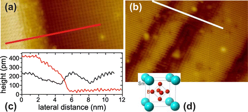
In Figure an overview of the different surfaces encountered so far is presented. It should be emphasised that these different topographies may come in various sizes (they can be as small as a few nm) and may coexist on one and the same surface depending on the investigated location. In STS, spectroscopy can be conducted on a well-defined topography while measurements in which a certain area is investigated (e.g. ARPES, optical conductivity or point contact measurements) may very well average over different terminations with unknown weight. The upper central image of Figure presents a Sm-terminated surface. This can most easily be recognised by considering the main crystallographic directions (shown on the left side): the lines of corrugations run along the diagonal. This is obvious from the zoom on the left [Citation20] which shows an area of nm
. The Sm atoms (blue circles) exhibit the expected square arrangement along the main crystallographic directions and with correct distances (SmB
: cubic crystal structure with lattice constant
4.133 Å, cf. Figure (d)). In addition, also the apex of the B octahedra (pink) is clearly seen in the topography (the assignment of the atoms will become clear below). The dark dents likely represent Sm atoms missing from the uppermost layer; in this case their depth of about 70 pm is in line with expectations from the crystal structure. Very similar surface structures were observed on SmB
[Citation21] as well as LaB
[Citation22]. In contrast, the two topographies at bottom left and centre depict
Figure 1. (colour online) Overview of the different topographies encountered for planes. Notes. The upper left and centre topographies present Sm-terminated surfaces; the main crystallographic directions are indicated. The zoom on the left shows an area of
nm
, with the Sm (blue) and B (pink) apex atoms marked by circles [Citation20]; cf. Figure for the crystal structure and heights of corrugations for the respective terminations. The bottom left and centre topographies exhibit B-termination; the centre one adumbrates electronic inhomogeneity (left topography:
0.1 V,
0.4 nA,
0.35 K). The two images on the right depict reconstructed surfaces; the upper one disordered, the lower one ordered (
reconstruction). See Section 3.3 for discussion. White lines indicate a main crystallographic direction, heights are very similar to those of Figure (g).
![Figure 1. (colour online) Overview of the different topographies encountered for planes. Notes. The upper left and centre topographies present Sm-terminated surfaces; the main crystallographic directions are indicated. The zoom on the left shows an area of nm, with the Sm (blue) and B (pink) apex atoms marked by circles [Citation20]; cf. Figure 2 for the crystal structure and heights of corrugations for the respective terminations. The bottom left and centre topographies exhibit B-termination; the centre one adumbrates electronic inhomogeneity (left topography: 0.1 V, 0.4 nA, 0.35 K). The two images on the right depict reconstructed surfaces; the upper one disordered, the lower one ordered ( reconstruction). See Section 3.3 for discussion. White lines indicate a main crystallographic direction, heights are very similar to those of Figure 3(g).](/cms/asset/b043f4fd-173e-48f6-92d0-b6c67bb33f0f/tphm_a_1171414_f0001_oc.gif)
B-terminated areas. Here, the corrugations are aligned parallel to the 1 0 0
directions (indicated by a white line in the centre image). However, the centre image clearly shows some underlying inhomogeneities (also seen in [Citation23]) which are not present in the left image. We consider this inhomogeneity to be electronic in origin and discussed this below. The two images on the right visualise differently reconstructed surfaces. The upper one shows that the Sm atoms on top of the B surface do not necessarily need to order into a (
) reconstruction as it is presented in the lower image (for further discussion, see Section 3.3). Some of the surface terminations reported here have also been observed by others [Citation21,Citation23]. It should be noted, however, that all these smooth terminations need often to be searched for, while many areas appear rough on an atomic scale.
A topography exhibiting a step edge is presented in Figure (a). The total height of this step, 0.41 nm, is in excellent agreement with the lattice constant. However, this step is rather broad (see also the height scan (red curve) in Figure (c) taken along the red line in Figure (a)), an observation we typically encountered for the few step edges found so far. This may indicate a distorted lattice structure along the ridge, in line with the above-mentioned observation that smooth terminations were rather infrequent. Alternatively, other terminations involving breaking up of intra-octahedral bonds (see below) might also be encountered along the step edge. All these possibilities, however, call for locally resolved spectroscopic measurements.
3.2. Assignment of the surface termination
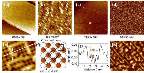
In all discussions about the different surfaces it is pivotal to assign the termination properly, i.e. to unambiguously distinguish Sm- from B-termination. The likely most reliable way to achieve this is by the observation of
Figure 2. (colour online) (a) Step of one unit cell height on a non-reconstructed surface (area shown: nm
). This step is not sharp but rather extended. (b) Non-reconstructed surface (
nm
) on a different sample exhibiting several steps between Sm- and B-terminated areas. The white line is almost parallel to a
1 0 0
crystallographic direction. (c) Height scans along the marked lines; red curve relates to red line in (a), black curve to white line in (b). (d) Cubic crystal structure of SmB
.
atomically resolved steps separating different terminations, and specifically if these step heights are in agreement with expectations from the crystal structure [Citation20]. Here, further support to this assignment is presented; this time by considering steps between alternating surface terminations as presented in the topography Figure (b). In this nm
field of view, three ‘trenches’ of approximately 100 pm in depth can clearly be made out, see height scan (Figure (c), black line) along the white line marked in the topographic image. Note that this height scan was taken almost parallel to one of the main crystallographic directions, i.e. along
1 0 0
. We assign the upper (brighter in Figure (b)) terraces to Sm-terminated areas and the lower (darker) ones to B terminations for the following two reasons: (i) The height difference of the upper and lower terraces corresponds approximately to the distance between the centre of a B atom and the plane spanned by the four closest Sm atoms, i.e. half the distance of two inter-octahedral borons (0.083 nm). Of course, the heights as measured by STM are also influenced by the local density of states (DOS) and possibly also by some relaxation of the surface atom distances with respect to their bulk distances. In addition, the steps are again not sharp, as discussed above for Figure (a). Nonetheless, the measured heights are difficult to explain for any other assumed surface configuration. (ii) As already seen for the non-reconstructed surfaces in Figure , the corrugations on the upper terraces run along lines parallel to
1 1 0
(note that the white line in Figure (b) is almost parallel to
1 0 0
). These corrugations have slightly alternating heights corresponding to an alternating visualisation of Sm and B atoms with distances of
along the diagonal [Citation20]. In contrast, the corrugations within the lower areas of Figure (b) are oriented along
1 0 0
with distances of a as expected if apex atoms of the B octahedra are visualised.
Within the cubic crystal structure of SmB, the octahedra form sturdy B
polymeric anions. Yet, the inter-octahedral B-distance (0.1669 nm) is slightly smaller than the intra-octahedral distance (0.1744 nm) [Citation24]. Hence, one might consider cleaving through the B
octahedra rather than between them. Indeed, we rarely observed ‘doughnut-shaped’ structures (see Figure (h)), similar to those reported in [Citation21]. These ‘doughnuts’ have diameters of about one lattice constant and therefore, are likely made up by eight boron atoms, i.e. two respective atoms out of each of four adjacent octahedra, cf. Figure (d) for the SmB
unit cell and [Citation21]. In order to rationalise the experimental findings, i.e. compare cleaving by breaking inter-octahedral vs. intra-octahedral bonds, electronic structure calculations with respect to the surface energies
of differently terminated slabs were carried out. Density functional theory calculations in the generalised gradient approximation were conducted for LaB
and CaB
, i.e. two hexaborides with integer valence La
and Ca
next to the intermediate valence
2.6 of SmB
. The implementation in the all-electron first principles code FHI-AIMS was employed using localised, numerically tabulated atom-centred orbitals [Citation25]. For LaB
the calculated values are in good agreement with [Citation26]: an energetic preference of the surface formed by cutting the inter-octahedral boron bonds (
Jm
), as compared to surfaces that cut intra-octahedral bonds (
Jm
), was found. For the case of CaB
, the difference is somewhat larger (2.77 Jm
and 3.92 Jm
, respectively). Surface relaxations do not yield substantial changes and decrease all mentioned surface energies by 0.1–0.2 Jm
. Assuming that qualitatively the same picture holds for SmB
, the calculations support the assertion above that in rare cases, e.g. in concert with respective lattice imperfections, the cleavage can also take place between intra-octahedral bonds, while in the typical case the cleaving is expected to leave the B octahedra intact.
The surface structure of Figure (b) can be compared to the () reconstructed surface (Figure lower right): in both cases, Sm- and B-terminated surfaces are exposed simultaneously but on different length scales. Yet, tunneling spectra obtained on reconstructed surfaces clearly differ from those on non-reconstructed ones [Citation20,Citation23]. Spectra obtained on unreconstructed Sm- and B-terminated surfaces were compared in [Citation20]: the size of the hybridisation gap agrees for both terminations, as anticipated for a bulk property. On the other hand, one obvious difference is that tunneling into quasiparticle states is more pronounced on Sm-terminated surfaces. The latter is in line with expectations and provides further support to our assignment of surface terminations. However, taking all this together emphasises again the need for detailed local information on the exact surface structure.
3.3. Atomically reconstructed surfaces
As already mentioned, a bulk truncated 0 0 1
surface of SmB
is polar due to uncompensated charges at the
Figure 3. (colour online) (a)–(d) STM images of cleaved 0 0 1
surface of SmB
. While (a), (b) and (d) are disordered, an ordered (
) reconstruction can be recognised in (c). (e) High resolution image
of a disordered surface similar to (a), where Sm atoms form a self-organised labyrinth on top of a
reconstructed B-terminated surface. Notice that across the Sm chains B
octahedra are anti-phase with each other (for example, see white arrows). (f) Schematic diagram of a
reconstructed B-terminated surface. Empty black (solid brown) circles represent missing (filled) B
octahedra. (g) Line scan along the white line in (e). (h) High resolution zoomed
image of (d) displaying doughnut-like features. Heights of corrugations in (a)–(c) are very similar to (e), total height scales in (d) and (h) are 0.12 nm.
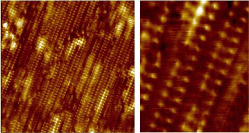
surface. The intermediate valence of Sm renders a simple electron counting even more complicated. However, several reasons may give rise to complex surface morphologies, such as a concomitant reduction of the free energy [Citation27] and/or an accommodation of the strain induced by the atomic size mismatch of the constituents [Citation28]. In consequence, a variety of differently reconstructed surfaces was reported based on atomically resolved STM [Citation20,Citation21,Citation23]. In Figure (a)–(d), the STM images of 0 0 1
surfaces on areas as large as
nm
are presented. Such atomically reconstructed regions can extend up to a few microns. A single cleave at low temperatures can produce all these different types of topographies indicating that they all lie close in energy. The topographic images in Figure (a), (b) and (d) are disordered, whereas (c) displays an ordered (2
1) reconstruction (cf. also Figure right). The latter type of reconstruction was observed previously in STM and low-energy electron diffraction measurements [Citation29,Citation30].
The surface displayed in Figure (a) is particularly interesting: here, Sm atoms form a self-organised labyrinth-like structure on a reconstructed B-terminated surface. In Figure (e), a high resolution image of a similar surface is presented. Across the Sm-chain, the B
octahedra are shifted by half a unit cell, i.e. they are anti-phase with respect to each other. In Figure (f) a schematic diagram of such a
reconstruction is presented, in which the missing B
octahedra are represented by black circles. These reconstructions are also found in the mixed-valent material Fe
O
[Citation31]. A height scan along the white line in Figure (e) can be seen in Figure (g). The Sm–Sm valley-height with respect to that of B
–B
is found to be 0.078 nm, which is comparable to the distance of 0.083 nm between the top B-atom of the B
octahedra and the plane made up by the four closest Sm atoms in the SmB
unit cell (i.e. half the inter-octahedra distance). Further, the B
–B
distance 0.56 nm is close to
, which is consistent with a
-type reconstruction. Figure (h) depicts a high resolution zoom-in image of (d). This disordered surface is likely comprised of both Sm as well as B atoms. Similar doughnut-like features have been reported in [Citation21].
It is needless to mention that the surface reconstructions may easily result in even more complex surface states, which make a straightforward observation of the topologically non-trivial surface states an experimental challenge. A well-known example for the formation of a metallic surface layer is the Si(1 1 1) reconstruction [Citation32].
4. Surfaces along the 1 1 0 plane
In contrast to the 1 0 0
surface discussed in Section 3, the
1 1 0
surface of SmB
is not polar. Hence, one could expect that an interpretation of results obtained on the latter is more straightforward. For the
1 1 0
surface, two additional surface Dirac points were predicted [Citation33]. Also, experimental results obtained on cleaved
1 1 0
surfaces have been reported [Citation34,Citation35].
Different areas of a cleaved 1 1 0
surface are presented in Figure . Clearly, atomic
Figure 4. (colour online) STM images of a cleaved 1 1 0
surface of SmB
; left:
nm
, right:
nm
. Although atomic corrugations can clearly be recognised, these surfaces are not as smooth as those obtain for
0 0 1
planes.
resolution is achieved and the rectangular arrangement expected for Sm atoms on a 1 1 0
plane with correct distances is seen in the zoomed-in image. However, the surfaces appear certainly not as smooth as those obtained on
0 0 1
surfaces, contain numerous defects and therefore, likely, different types of atoms and may exhibit locally varying atomic environments. Consequently, care has to be taken in interpreting spectroscopic results unless the quality of the surfaces is improved.
5. Electronic inhomogeneities at the surface
In the following we focus on 0 0 1
surfaces which are not atomically reconstructed. Spectroscopy on smaller (a few nm in extent) non-reconstructed areas revealed indications for the hybridisation gap [Citation20] expected for a Kondo insulator at low temperatures. In contrast, on larger areas – at least several tens of nm in extent – the tunneling spectral line-shape typically appeared as a Fano resonance [Citation36], owing to a quantum mechanical interference of the electrons tunneling from (to) the STM tip into (out of) the quasiparticle states and the conduction band. Then, the tunneling conductance g(V) = dI(V)/dV can be fitted by [Citation37]
(1)
Here, and
are the width of the resonance and its position in energy, respectively. The asymmetry parameter q is determined by the probabilities of tunneling into the quasiparticle states and the conduction band, as well as by the particle-hole asymmetry [Citation38]. Although the bare local DOS of SmB
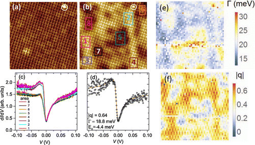
is obscured by the
Figure 5. (colour online) Topography of B-terminated SmB over an area of
nm
measured at 6 K using a dual bias mode: (a) Forward scan with
V and (b) backward scan with
V. An impurity marked by white circles confirms that both images were taken on the same area. (c) Average tunneling conductance g(V) on areas marked by matching colours in (b). (d) Typical single tunneling spectrum and corresponding fit (continuous line) to Equation (Equation1
(1) ). (e) and (f) Spatial variation of
and |q|, respectively.
Fano resonance, the parameter can be related to the Kondo temperature
[Citation39].
The STM topography, as shown in Figure (a), was conducted on a B-terminated area of nm
in a dual bias mode. This implies that the same area can be scanned with two different bias voltages applied for the forward and backward scans. In the present case, the forward scan was conducted with
V, Figure (a), while
V was used for the backward scan in Figure (b). The fact that exactly the same areas were visualised is evidenced by the impurity marked by the white circles in Figure (a) and (b). Nonetheless, a strong spatial inhomogeneity is seen in Figure (b), which is not present in Figure (a). Since the tunneling conductance is a convolution of tip–sample distance and the local DOS, this suggests not only a spatially inhomogeneous but also a asymmetric local DOS with respect to the sign of
. This can be more clearly inferred from the tunneling conductance presented in Figure (c). Here, the dI/dV-curves were obtained by averaging over the areas shown in (b) with matching colours. These curves differ significantly between
0 mV. All 2500 individual spectra obtained within the field of view of Figure (a) and (b) were fitted to Equation (Equation1
(1) ); an example is given in Figure (d). The resulting spatial maps for
and |q| are presented in Figure (e) and (f), respectively. Notably,
and |q| are anti-correlated, i.e. the regions with larger values of
exhibit smaller values of |q|. This is consistent since larger values of
suggest stronger hybridisation. Because the hybridisation in SmB
takes place between Sm 4f states and the 5d conduction band [Citation8], a large
may imply that the 5d bands are more occupied, which in turn can give rise to a higher probability of tunneling into the conduction band, i.e. smaller |q|, particularly on a B-terminated surface as shown here. We speculate that the spatial inhomogeneities of
and |q| are related to a spatially inhomogeneous intermediate valence of Sm at the surface of SmB
.
Within our field of view, is found to vary between
meV
1 meV, with a pronounced maximum of probability at
meV. Since the hybridisation gap in SmB
is about 15–20 meV [Citation13,Citation20,Citation40,Citation41], one may assume that the Fano resonance found here is likely a phenomenon related to the in-gap states lying close to the Fermi level
. As mentioned above, in order for the Fano resonance to show up, two types of tunneling channels are required. One may then speculate about the two contributions changing locally, i.e. the heavy quasiparticles related to the bulk and the conduction band being related to the surface states, both of which reside inside the hybridisation gap. Evidence for the former is found in specific heat [Citation42] and recent ARPES measurements [Citation19]. The latter may have been detected in de Haas–van Alphen experiments, which report two-dimensional Fermi surfaces with light effective mass of the quasiparticles [Citation43], a view which, however, has been challenged [Citation35].
6. Kondo effect
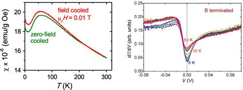
As mentioned above, SmB is an intermediate-valence
Figure 6. (colour online) Left: Temperature dependence of the susceptibility . Right: Tunneling spectra on a B-terminated surface of SmB
at temperatures 6 K
50 K clearly showing Fano-type line-shapes and a closing-up of the partial gap at zero-bias with increasing T.
compound with a Sm valence of [Citation44]. For such a value of
it is questionable to what extent the standard Kondo picture can be applied [Citation45].
In Figure left, the susceptibility is recapped for one of our samples. In line with earlier measurements [Citation7,Citation13,Citation46] it exhibits Curie–Weiss-like and van Vleck contributions (due to its intermediate valence) for K, and non-magnetic behaviour with an enlarged DOS at
at lowest temperatures. The upturn at lowest temperatures which is typically assigned to paramagnetic impurities [Citation7,Citation46,Citation47] is comparatively tiny for this SmB
sample indicating excellent sample quality. Nonetheless, one might speculate that the small difference in
between zero-field and field cooled measurement may be due to this tiny amount of impurities.
Whether or not the overall behaviour is related to an underlying Kondo effect has been discussed controversially, see e.g. [Citation6,Citation7,Citation48,Citation50]. More recent support for the Kondo picture was provided e.g. by the analysis of point contact measurements [Citation13]. The closing-up of the gap as observed by temperature dependent STS measurements on small, non-reconstructed surface areas was also consistent with expectations for the Kondo effect [Citation20]. In Figure right, g(V)-spectra obtained on a large, non-reconstructed B-terminated area in the range 6 K 50 K is presented. In contrast to [Citation20], the spectra here are clearly of Fano-type. Yet, the closing of the (partial) gap with increasing temperature follows the same trend and hence, is again consistent with a logarithmic behaviour expected for the Kondo effect [Citation51]. Note that very similar Fano line-shapes were obtained on a (
) reconstructed surface in the temperature range 8 K
30 K and the respective spectra were interpreted in terms of hybridisation resulting from the underlying Kondo lattice [Citation23].
Acknowledgements
The authors gratefully acknowledge experimental help by Tae-Hwan Jang and insightful discussions with Yuri Grin.
Additional information
Funding
Notes
No potential conflict of interest was reported by the authors.
References
- M.Z. Hasan and C.L. Kane, Colloquium: Topological insulators, Rev. Mod. Phys. 82 (2010), pp. 3045–3067.
- A. Stern, D.K. Efimkin, V. Galitski, J. Xia, and Z. Fisk, Radio frequency tunable oscillator device based on SmB6 micro-crystal, (2015). Available at arXiv:1510.02569.
- C.L. Kane and E.J. Mele, Z2 topological order and the quantum spin Hall effect, Phys. Rev. Lett. 95 (2005), pp. 146802-1–146802-4.
- L. Fu and C.L. Kane, Topological insulators with inversion symmetry, Phys. Rev. B 76 (2007), pp. 045302-1–045302-17.
- M. Dzero, K. Sun, V. Galitski, and P. Coleman, Topological Kondo insulators, Phys. Rev. Lett. 104 (2010), pp. 106408-1–106408-4.
- G. Aeppli and Z. Fisk, Kondo insulators, Comments Condens. Matter. Phys. 16 (1992), pp. 155–165.
- P.S. Riseborough, Heavy fermion semiconductors, Adv. Phys. 49 (2000), pp. 257–320.
- T. Takimoto, SmB6: A promising candidate for a topological insulator, J. Phys. Soc. Jpn. 80 (2011), pp. 123710-1–123710-4.
- F. Lu, J.Z. Zhao, H. Weng, Z. Fang, and X. Dai, Correlated topological insulators with mixed valence, Phys. Rev. Lett. 110 (2013), pp. 096401-1–096401-5.
- V. Alexandrov, M. Dzero, and P. Coleman, Cubic topological Kondo insulators, Phys. Rev. Lett. 111 (2013), pp. 226403-1–226403-5.
- J. Kim, K. Kim, C.-J. Kang, S. Kim, H.C. Choi, J.-S. Kang, J.D. Denlinger, and B.I. Min, Termination-dependent surface in-gap states in a potential mixed-valent topological insulator: SmB6, Phys. Rev. B 90 (2014), pp. 075131-1–075131-6.
- S. Wolgast, C. Kurdak, K. Sun, J.W. Allen, D.J. Kim, and Z. Fisk, Low-temperature surface conduction in the Kondo insulator SmB6, Phys. Rev. B 88 (2013), pp. 180405(R)-1–180405(R)-5.
- X. Zhang, N.P. Butch, P. Syers, S. Ziemak, R.L. Greene, and J. Paglione, Hybridization, correlation, and in-gap states in the Kondo Insulator SmB6, Phys. Rev. X 3 (2013), pp. 011011-1–011011-7.
- D.-J. Kim, S. Thomas, T. Grant, J. Botimer, Z. Fisk, and J. Xia, Surface Hall effect and nonlocal transport in SmB6: Evidence for surface conduction, Sci. Rep. 3 (2013), pp. 3150-1–3150-4.
- N. Xu, P.K. Biswas, J.H. Dil, R.S. Dhaka, G. Landolt, S. Muff, C.E. Matt, X. Shi, N.C. Plumb, M. Radovic, E. Pomjakushina, K. Conder, A. Amato, S.V. Borisenko, R. Yu, H.-M. Weng, Z. Fang, X. Dai, J. Mesot, H. Ding, and M. Shi, Direct observation of the spin texture in SmB6 as evidence of the topological Kondo insulator, Nat. Commun. 5 (2014), pp. 4566-1–4566-5.
- S. Suga, K. Sakamoto, T. Okuda, K. Miyamoto, K. Kuroda, A. Sekiyama, J. Yamaguchi, H. Fujiwara, A. Irizawa, T. Ito, S. Kimura, T. Balashov, W. Wulfhekel, S. Yeo, F. Iga, and S. Imada, Spin-polarized angle-resolved photoelectron spectroscopy of the so-predicted Kondo topological insulator SmB6, J. Phys. Soc. Jpn. 83 (2014), pp. 014705-1–014705-6.
- Z.-H. Zhu, A. Nicolaou, G. Levy, N.P. Butch, P. Syers, X.F. Wang, J. Paglione, G.A. Sawatzky, I.S. Elfimov, and A. Damascelli, Polarity-driven surface metallicity in SmB6, Phys. Rev. Lett. 111 (2013), pp. 216402-1–216402-5.
- E. Frantzeskakis, N. de Jong, B. Zwartsenberg, Y.K. Huang, Y. Pan, X. Zhang, J.X. Zhang, F.X. Zhang, L.H. Bao, O. Tegus, A. Varykhalov, A. de Visser, and M.S. Golden, Kondo hybridization and the origin of metallic states at the (001) surface of SmB6, Phys. Rev. X 3 (2013), pp. 041024-1–041024-11.
- P. Hlawenka, K. Siemensmeyer, E. Weschke, A. Varykhalov, J. Sánchez-Barriga, N.Y. Shitsevalova, A.V. Dukhnenko, V.B. Filipov, S. Gabáni, K. Flachbart,O. Rader, and E.D.L. Rienks, Samarium hexaboride: A trivial surface conductor, (2015). Available at arXiv:1502.1542.
- S. Rößler, T.-H. Jang, D.-J. Kim, L.H. Tjeng, Z. Fisk, F. Steglich, and S. Wirth, Hybridization gap and Fano resonance in SmB6, Proc. Nat. Acad. Sci. USA 111 (2014), pp. 4798–4802.
- W. Ruan, C. Ye, M. Guo, F. Chen, X. Chen, G.-M. Zhang, and Y. Wang, Emergence of a coherent in-gap state in the SmB6 Kondo insulator revealed by scanning tunneling spectroscopy, Phys. Rev. Lett. 112 (2014), pp. 136401-1–136401-5.
- J.S. Ozcomert and M. Trenary, Atomically resolved surface structure of LaB6(100), Surf. Sci. Lett. 265 (1992), pp. L227–L232.
- M.M. Yee, Y. He, A. Soumyanarayanan, D.-J. Kim, Z. Fisk, and J.E. Hoffman, Imaging the Kondo insulating gap on SmB6, (2013). Available at arXiv:1308.1085.
- I.D.R. Mackinnon, J.A. Alarco, and P.C. Talbot, Metal hexaborides with Sc, Ti or Mn, Model. Numer. Simul. Mater. Sci. 3 (2013), pp. 158–169.
- V. Blum, R. Gehrke, F. Hanke, P. Havu, V. Havu, X. Ren, K. Reuter, and M. Scheffler, Ab initio molecular simulations with numeric atom-centered orbitals, Comput. Phys. Commun. 180 (2009), pp. 2175–2196.
- M.A. Uijttewaal, G.A. de Wijs, and R.A. de Groot, Ab initio and work function and surface energy anisotropy of LaB6, J. Phys. Chem. B 110 (2006), pp. 18459–18465.
- H. Röder, R. Shuster, H. Brune, and K. Kern, Monolayer-confined mixing at the Ag--Pt(111) interface, Phys. Rev. Lett. 71 (1993), pp. 2086–2089.
- J. Tersoff, Surface-confined alloy formation in immiscible systems, Phys. Rev. Lett. 74 (1995), pp. 434–437.
- M. Aono, R. Nishitani, T. Tanaka, E. Bannai, and S. Kawai, Azimuthal anisotropy in low-energy ion scattering from SmB6 (001), Solid State Commun. 28 (1978), pp. 409–412.
- H. Miyazaki, T. Hajiri, T. Ito, S. Kunii, and S.-I. Kimura, Momentum-dependent hybridization gap and dispersive in-gap state of the Kondo semiconductor SmB6, Phys. Rev. B 86 (2012), pp. 075105-1–075105-4.
- N. Stanka, W. Hebenstreit, U. Diebold, and S.A. Chambers, Surface reconstruction of Fe3O4(001), Surf. Sci. 448 (2000), pp. 49–63.
- K. Yoo and H.H. Weitering, Electrical conductance of reconstructed silicon surfaces, Phys. Rev. B 65 (2002), pp. 115424-1–115424-11.
- M. Ye, J.W. Allen, and K. Sun, Topological crystalline Kondo insulators and universal topological surface states of SmB6, (2013). Available at arXiv:1307.7191.
- F. Chen, C. Shang, Z. Jin, D. Zhao, Y.P. Wu, Z.J. Xiang, Z.C. Xia, A.F. Wang, X.G. Luo, T. Wu, and X.H. Chen, Magnetoresistance evidence of a surface state and a field-dependent insulating state in the Kondo insulator SmB6, Phys. Rev. B 91 (2015), pp. 205133-1–205133-5.
- B.S. Tan, Y.-T. Hsu, B. Zeng, M.C. Hatnean, N. Harrison, Z. Zhu, M. Hartstein, M. Kiourlappou, A. Srivastava, M.D. Johannes, T.P. Murphy, J.-H. Park, L. Balicas, G.G. Lonzarich, G. Balakrishnan, and S.E. Sebastian, Unconventional Fermi surface in an insulating state, Science 349 (2015), pp. 287–290.
- U. Fano, Effects of configuration interaction on intensities and phase shifts, Phys. Rev. 124 (1961), pp. 1866–1879.
- A. Schiller and S. Hershfield, Theory of scanning tunneling spectroscopy of a magnetic adatom on a metallic surface, Phys. Rev. B 61 (2000), pp. 9036–9046.
- J. Figgins and D.K. Morr, Differential conductance and quantum interference in Kondo systems, Phys. Rev. Lett. 104 (2010), pp. 187202-1–187202-4.
- K. Nagaoka, T. Jamneala, M. Grobis, and M.F. Crommie, Temperature dependence of a single Kondo impurity, Phys. Rev. Lett. 88 (2002), pp. 077205-1–077205-4.
- B. Gorshunov, N. Sluchanko, A. Volkov, M. Dressel, G. Knebel, and A. Loidl, Low-energy electrodynamics of SmB6, Phys. Rev. B 59 (1999), pp. 1808–1814.
- M. Neupane, N. Alidoust, S.-Y. Xu, T. Kondo, Y. Ishida, D.-J. Kim, C. Liu, I. Belopolski, Y.J. Jo, T.-R. Chang, H.-T. Jeng, T. Durakiewicz, L. Balicas, H. Lin, A. Bansil, S. Shin, Z. Fisk, and M.Z. Hasan, Surface electronic structure of the topological Kondo-insulator candidate correlated electron system SmB6, Nat. Commun. 4 (2013), pp. 2991-1–2991-7.
- S. Gabáni, K. Flachbart, E. Konovalova, M. Orendáč, Y. Paderno, V. Pavlík, and J. Šebek, Properties of the in-gap states in SmB6, Solid State Commun. 117 (2001), pp. 641–644.
- G. Li, Z. Xiang, F. Yu, T. Asaba, B. Lawson, P. Cai, C. Tinsman, A. Berkley, S. Wolgast, Y.S. Eo, D.-J. Kim, C. Kurdak, J.W. Allen, K. Sun, X.H. Chen, Y.Y. Wang, Z. Fisk, and L. Li, Two-dimensional Fermi surfaces in Kondo insulator SmB6, Science 346 (2014), pp. 1208–1212.
- M. Mizumaki, S. Tsutsui, and F. Iga, Temperature dependence of Sm valence in SmB6 studied by X-ray absorption spectroscopy, J. Phys: Conf. Ser. 176 (2009), pp. 012034-1–012034-4.
- C.M. Varma, Aspects of strongly correlated insulators, Phys. Rev. B 50 (1994), pp. 9952–9956.
- S. Gabáni, K. Flachbart, V. Pavlík, T. Herrmannsdörfer, E. Konovalova, Y. Paderno, J. Briančin, and J. Trpčevská, Magnetic properties of SmB6 and Sm1-xLaxB6 solid solutions, Czech. J. Phys. 52 (2002), pp. A225–A228.
- S. Gabáni, K. Flachbart, V. Pavlík, E. Konovalova, Y. Paderno, and T. Herrmannsdörfer, Low temperature transport and magnetic properties of SmB6, Acta Phys. Pol. 97 (2000), pp. 419–422.
- J.C. Cooley, M.C. Aronson, Z. Fisk, and P.C. Canfield, SmB6: Kondo insulator or exotic metal? Phys. Rev. Lett. 74 (1995), pp. 1629–1632.
- B.R. Coles, Speculations concerning SmB6, Physica B 230–232 (1997), pp. 718–720.
- T. Kasuya, Physical mechanism in Kondo insulator, J. Phys. Soc. Jpn. 65 (1996), pp. 2548–2558.
- T.A. Costi, Kondo effect in a magnetic field and the magnetoresistivity of Kondo alloys, Phys. Rev. Lett. 85 (2000), pp. 1504–1507.