
 ?Mathematical formulae have been encoded as MathML and are displayed in this HTML version using MathJax in order to improve their display. Uncheck the box to turn MathJax off. This feature requires Javascript. Click on a formula to zoom.
ABSTRACT
The purpose of the present study was to provide a reliable value for the specific grain-boundary resistivity ρSGBR of Ni metal. New results are presented on the room-temperature electrical resistivity of nanocrystalline (nc) Ni metal samples produced by electrodeposition with various grain sizes. These resistivity data were compared with previous reports on nc-Ni and all results were analysed according to the procedure of Andrews [Phys. Lett. 19, 558 (1965)] who found that the resistivity increment due to grain boundaries is proportional to the grain-boundary surface area per unit volume which is, on the other hand, inversely proportional to the grain size. It is pointed out that the grain size directly accessible by transmission electron microscopy imaging is the relevant parameter for the evaluation of ρSGBR whereas the crystallite size deduced from X-ray diffraction line broadening leads to an underestimation of ρSGBR because coherency-breaking intragrain defects not contributing significantly to the resistivity also cause a line broadening. From the evaluation of the nc-Ni resistivity data at room temperature, we find that 4.45·10−16 Ω·m2 < ρSGBR(Ni) < 6.2·10−16 Ω·m2 and our upper bound agrees exactly with the most recent calculated value in the literature.
1. Introduction
At finite temperatures, the electrical resistivity of a single-crystal pure metal is determined by the lattice contribution due to the electron–phonon scattering [Citation1]. By converting the single crystal into a polycrystal, various structural defects are introduced into the lattice. The lattice defects, due to their positional disorder (short-range effect), represent additional electron scattering centres for the conduction electrons and this leads to an increase of the resistivity at any temperature, even at T = 0 K [Citation1]. We will restrict ourselves to the presence of grain boundaries as the only (or dominating) lattice defect type. For this particular case, Ziman [Citation1] suggested that, due to the orientational misfit between two neighbouring grains (long-range effect), we can consider that an electron arriving at a grain boundary can undergo a scattering event also as a consequence of the change of its wave vector direction with respect to the crystal axes (we may call it also orientational effect). In the case of the short-range effect, the grain boundaries as lattice defects can be represented by a scattering potential of a given amplitude (scattering strength) and spatial width (the thickness of a grain boundary is determined by the number of atomic layers which appear as perturbed atomic planes with respect to the perfect crystal on both sides of the grain-boundary core). Concerning the long-range (or orientational) effect, it can be treated by considering the anisotropy of the Fermi surface of the metal.
Lormand [Citation2] gave a summary of early theoretical attempts to take into account the two ways grain boundaries influence the resistivity, concluding that probably the orientational effect may be the dominating one in determining the contribution of grain boundaries to the resistivity.
To test the theoretical approaches, experimental data are needed for the grain-boundary contribution to the resistivity. The first successful attempt in this direction was made by Andrews [Citation3] who noticed that the resistivity increased linearly with the grain-boundary surface area per unit volume (SGB/V). In particular, he introduced the concept of the specific grain-boundary resistivity ρSGBR and also determined its value for Cu. This study was followed by the works of Andrews et al. [Citation4] on Cu and Al, Kasen [Citation5] on Al and Mannan and Karim [Citation6] on Cu; subsequent early data on various polycrystalline metals have been collected in several reviews [Citation2,Citation7,Citation8].
In the early 1990s, Nakamichi and co-workers [Citation9] demonstrated that by using a SQUID device, one can measure the resistivity contribution of a single grain boundary. They could also show that the specific grain-boundary resistivity depends on the type of grain boundary (twist and orientation between the grains separated by the given boundary). They concluded from this finding that the grain-boundary resistivity is mainly caused by the electron scattering from the core region of the grain boundary. We believe that this conclusion is not necessarily valid since, evidently, not only the short-range effect (influence of boundary core region as scattering source), but also the above discussed orientational effect changes with the degree of the misorientation.
In the meantime, progress has been made also on the theoretical side in that the resistivity of a single grain boundary could be derived by first-principles calculations [Citation7,Citation10,Citation11]. Further theoretical work along this line is necessary to shed more light on the relative importance of the short-range effect and the orientational effect in the total grain-boundary resistivity.
Since the measurement of the resistivity of a single grain boundary [Citation9] is not an easy task and requires the preparation of a specific bicrystal, most of the grain-boundary resistivity data have been collected on polycrystalline metals. Therefore, the experimentally derived value of the specific grain-boundary resistivity for a polycrystalline metal usually represents a mean value only which is an average over all types of grain boundaries present in the investigated sample. In these studies, the grain sizes were typically in the micrometer range. In order to determine the relatively small grain-boundary contribution, it usually required to carry out the resistivity measurements at very low temperature where the large phonon contribution background is suppressed. On the other hand, by using a nanocrystalline (nc) metal specimen with grain sizes below about 100 nm, the volume fraction of grain boundaries can be so high that the grain-boundary contribution to the total resistivity can be successfully measured even at room temperature.
Specifically for Ni metal, there have been several studies on the resistivity for the nanocrystalline state (see, e.g. Refs. Citation12–15). McCrea et al. [Citation14] have demonstrated for electrodeposited nc-Ni that the linear increase of the resistivity with increasing SGB/V, as observed by Andrews [Citation3] in the micrometer range of grain sizes for Cu metal, persists for Ni in the nanometric grain size range as well. From this analysis, McCrea et al. [Citation14] deduced a value of ρSGBR(Ni,295K) = 2.74·10−16 Ω·m2.
Recently, we have presented a detailed structural characterisation of electrodeposited nc-Ni with various grain sizes [Citation16,Citation17] by X-ray diffraction (XRD) and/or transmission electron microscopy (TEM). The work of McCrea et al. [Citation14] instigated us to carry out a similar study on the room-temperature electrical resistivity of these nc-Ni foils and to perform the same analysis of the resistivity data, by including also all nc-Ni resistivity data reported beforehand in the literature.
This paper is organised as follows. Section 2 is devoted to a description of the evaluation scheme used for deducing ρSGBR from the experimental resistivity data as a function of grain size. In Section 3, the investigated Ni samples, their structural characterisation and the measurement techniques will be described. Our new experimental results on the room-temperature electrical resistivity on nc-Ni are presented in Section 4. The extraction of ρSGBR(Ni) from all available resistivity data on nc-Ni will be carried out in Section 5, together with a discussion of all previous relevant data on Ni metal. A summary of the present study will be given in Section 6.
2. Evaluation scheme for deriving the specific grain-boundary resistivity
Our starting point is the approach of Andrews [Citation3] who found a contribution to the overall electrical resistivity that was proportional to the grain-boundary surface area (SGB) per unit volume, i.e. SGB/V. The resistivity increment due to the grain-boundary surface area per unit volume was then used to define the specific grain-boundary resistivity ρSGBR. Along this line, we can write the total resistivity of a metal as(1)
(1) where ρbulk is the resistivity of the defect-free state with large grains, at least in the micrometer range or above (this will be referred to as the bulk state) and
(2)
(2) is the total grain-boundary contribution to the resistivity. It is commonly accepted [Citation3–5,Citation7,Citation14] that SGB/V is inversely proportional to the average grain diameter d, i.e.
(3)
(3) with a constant proportionality factor kGB. We can write then for the total grain-boundary resistivity:
(4)
(4) where we have introduced the Andrews parameter A = kGB
·ρSGBR. Accordingly, we have for the total resistivity
(5)
(5) This formula should be used to fit the experimental data plotted as a function of d (or 1/d).
As to the proportionality constant kGB, various values were used depending on the particular considerations applied. Andrews et al. [Citation4] suggested kGB = 2.7, stressing that this is the commonly used value. McCrea et al. [Citation14] assumed that SGB/V can be calculated by using a tetrakaidecahedron as the grain shape. Based on the result of DeHoff and Rhines [Citation18], they derived this way a proportionality factor of kGB = 2.37. Brown [Citation7] took a different approach by using the results of Smith and Guttmann [Citation19] for a random three-dimensional structure of contiguous grains together with the results of Hensler [Citation20] for a wide range of size distributions of spherical grains. In this manner, Brown [Citation7] derived the proportionality factor kGB = 32/π2 ∼ 3.24, provided the grains are not severely elongated, i.e. they are nearly equi-axed.
By considering the uncertainty in the value of the proportionality factor kGB, we will proceed by fitting the experimental resistivity data to eq. (5) to determine the Andrews parameter A. Since A is the experimentally directly accessible parameter, being independent of any assumption, it is evident that when results of different works on a given metal are to be compared, it is the best to do the comparison on the basis of the fitted A values or we should use the same kGB factor to convert A to ρSGBR. The same holds true if we want to compare the results on two different metals. When comparing with theoretical ρSGBR values, the uncertainty of kGB persists in the experimental ρSGBR values as well; however, when converting A values of two metals to ρSGBR data by using the same kGB factor, the relation between the ρSGBR values of the two metals are preserved, so that a comparison with their calculated values is meaningful.
Along this line, we will mainly base the discussion of results on the experimentally derived A values and it will always be made clear which kGB value is used when converting A to ρSGBR. The analysis of the experimental data is carried out by plotting ρ against 1/d, then performing the fit to eq. (5) in order to determine A after which the data are shown in the form of ρ vs. d plots and displaying also the fit line.
3. Experimental
3.1. Samples investigated
The results of electrical transport measurements to be presented here were obtained on metallurgically processed as well as electrodeposited pure Ni metal foil samples. The metallurgically processessed samples (all corresponding to bulk Ni with large grain sizes and in an annealed state) were considered as reference only to demonstrate the accuracy of our resistivity measurements.
(i) Metallurgically processed Ni foils were prepared by cold rolling and annealing ingots from two different sources. After cold rolling in several steps down to a thickness between about 50 and 100 μm, the foils were exposed to a heat treatment at about 700°C for 1 h in a protecting hydrogen atmosphere to release the stresses introduced by the cold-rolling procedure. The samples prepared in this manner included the following Ni foils: sample #B5 prepared from electrolytic grade Ni and sample #Ni(99.99+%) prepared from a high-purity ingot.
Two further Ni foils were also included in the electrical transport studies: sample #GF-Ni(50 μm) of at least 99.6% purity and sample #GF-Ni(250 μm) of 99.98% purity, both foils purchased from Goodfellow Company with thicknesses as specified in the sample names.
(ii) Electrodeposition was used to prepare thin Ni foils on metallic substrates as described in Refs. Citation16 and Citation17. The substrates were then removed from the Ni deposits by mechanical stripping or electrochemical etching. Five of the nc-Ni samples investigated here were the same for which the structural properties were reported separately [Citation17]. Five more nc-Ni samples were also prepared under the same conditions for the present resistivity study and their structural characterisation was carried out in the same way. These ten electrodeposited (ED) Ni samples having a thickness of about 20 μm will be denoted as ED Ni series.
Two further ED Ni foil samples were also included in the present work: sample #B2 and sample #Ni(TKE) with a thickness of about 10 and 5 μm, respectively. These Ni samples were prepared for earlier studies reported in Ref. Citation21 under conditions described there.
Chemical analysis was carried out by energy-dispersive X-ray spectroscopy in a TESCAN MIRA3 scanning electron microscope equipped with an EDAX Element analyser on all the investigated Ni foils. Some C and O contamination was found for all samples which are very probably surface impurities only since they were detected in both the electrodeposited and the metallurgically processed samples roughly in the same amount. Besides C and O, no other non-metallic impurities were observed up to the detection limit (about 0.1 at.% in our method for elements with atomic number larger than 10) in all the Ni foil samples. In Ref. Citation12, a mass-spectrometric analysis of an ED nc-Ni sample with a grain size of the order of 50 nm yielded 0.35. at.% C impurity. Since elemental carbon can hardly be incorporated into the lattice of a metallic deposit during electrodeposition, if it is indeed present in the deposit, it is most probably present in the form of inclusions of organic additives used in the electrodeposition baths which, therefore, can hardly contribute to the resistivity. But even if we take, at the very extreme, this detected amount as dissolved in the lattice, we get a resistivity increment of 1 μΩcm only on the basis of available data on the influence of impurities on the resistivity of Ni. On the other hand, we will see later that the grain size refinement results in a resistivity increase by a factor of three over the bulk value (from the bulk value 7.24 μΩcm to about 20 μΩcm at around 10 nm grain size). In electrodeposits, another non-metallic impurity, S is also often found for which the available resistivity increment data in a Ni matrix indicate a resistivity increase of about 3 μΩcm/at.%. Since we could not detect S above a level of 0.1 at.%, the resistivity increase due to S is at most 0.3 μΩcm. By considering that the above C contribution is certainly strongly overestimated, it turns out that the resistivity increment due to the possible non-metallic impurities is of the same size as our resistivity measurement error to be specified later in Section 4.1. Therefore, we should not really have a concern about the non-metallic impurities when analysing the grain size dependence of the resistivity in nc-Ni. As to the metallic impurities, two of the Ni samples in the ED Ni series contained about 3 at.% Co impurity which should be the result of the presence of Co impurity in the Ni-source chemical used to produce those two particular electrodeposited samples. The possible implication of the Co impurities on the resistivity of these nc-Ni samples will be discussed in Section 4.
3.2. Structural characterisation
3.2.1. Microstructure study: XRD vs. TEM
It was pointed out in Refs. Citation16 and Citation17 that one should make a clear distinction between the grain size d directly revealed by TEM image analysis and the crystallite size <x> that is derived from an XRD line-broadening study. We have found a correlation between the two kinds of size parameter [Citation17] in that the XRD crystallite size was smaller than the TEM grain size and this will have a consequence also on the analysis of the resistivity data as we will see later. Therefore, in the following, we will always make a clear distinction between d and <x>.
Whereas the determination of the grain size by the evaluation of dark-field TEM images is a fairly standard procedure [Citation16,Citation17], the derivation of the crystallite size corresponding to the average size of the coherently scattering domains by using the broadening of the XRD lines can be performed in several different ways [Citation22]. The simplest approach is the use of the Scherrer formula [Citation23] by deriving the crystallite size from the broadening of the major Bragg peak of the XRD pattern. The next step is the use of the classical Williamson-Hall plot [Citation23] when an extrapolation from the broadening of all measured XRD peaks is made to get the crystallite size. A more advanced evaluation is based on the modified Williamson-Hall analysis by taking into account the influence of dislocations on the broadening of individual Bragg peaks which method was specifically elaborated for nanocrystalline materials in the last two decades [Citation22,Citation24,Citation25]. The most powerful version of XRD studies of the microstructure is the whole-profile-fitting procedure in which the diffraction pattern is fitted by theoretical profiles related to the crystallite size and its distribution, dislocations and twin faults [Citation22].
3.2.2. TEM and XRD study of the microstructure of the ED Ni series samples
The microstructure of the ED Ni series samples was investigated both by direct TEM imaging and by XRD line profile analysis [Citation22] which methods are described in more detail in Refs. Citation16 and Citation17.
The microstructure was investigated by TEM using a Philips CM20 transmission electron microscope operated at an acceleration voltage of 200 kV. TEM images were taken in both planar and cross-sectional views, the latter studies carried out at both the substrate side and the solution side of the deposit foils. In order to achieve a combination of good resolution and high number of studied grains, for the grain size determination dark-field images were taken with a magnification of 50,000. The mean TEM grain size d was evaluated from the grain size distribution histograms obtained by averaging over about 1000 grains for both the electrolyte and substrate sides and for both the planar and cross-sectional views.
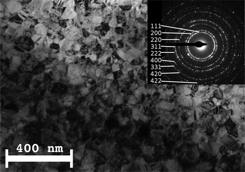
A bright-field TEM image and the corresponding SAED pattern are shown in for one sample of the ED Ni series which indicate the very fine-grained structure (see especially the numerous, almost continuous diffraction rings in the SAED patterns) of this Ni sample. As indicated in the figure caption, for this particular sample, the structural features of both the electrolyte and substrate sides of the deposit were the same.
Figure 1. Bright-field cross-sectional TEM image and indexed SAED pattern at the electrolyte side of the nc-Ni sample #FAC3 of the ED Ni series. The substrate side exhibited the same features.
Qualitatively, very similar results were obtained also for the other samples of the ED Ni series; where the structural features were different for the two sides of the deposit, the results were averaged. More details of the TEM sample preparation and the evaluation of the TEM results as well as TEM and XRD results for several of the samples included in the present resistivity study were described in Refs. Citation16 and Citation17. The TEM structural studies demonstrated that the ED Ni series samples are nanocrystalline.
The microstructure of the ED Ni series samples was investigated also by X-ray line profile analysis. The XRD patterns were measured by a RA-MultiMax9 rotating anode diffractometer using CuKα1 radiation with a wavelength of λ = 0.15406 nm. The diffractograms were evaluated by the extended Convolutional Multiple Whole Profile (eCMWP) fitting method [Citation22]. During this procedure, the diffraction peaks in the patterns were fitted by theoretical profile functions which were obtained as the convolution of the peaks caused by the finite crystallite size, dislocations and twin faults. The theoretical line profile related to the finite size of crystallites was calculated for spherical crystallites with a lognormal size distribution. The eCMWP procedure yields the median (m) and the lognormal variance (σ2) of the crystallite size distribution, the dislocation density and the twin fault probability, where the twin fault probability is defined as the fraction of twin boundaries among the (111) lattice planes. The arithmetically averaged crystallite size <x> (i.e. the mean of the size distribution) can be obtained from m and σ2 as <x> = m × exp(0.5 σ2). The details of the eCMWP procedure can be found in Refs. Citation16, Citation17 and Citation22. Because of the nano-grained microstructure of the studied samples, the physical broadening of the profiles was much higher than the instrumental broadening. Therefore, instrumental correction did not need to be applied in the evaluation. The mean XRD crystallite size <x> was deduced from the resulting fitted lognormal distributions.
(a) displays the measured XRD pattern and its fitting with the eCMWP procedure for the same sample for which the TEM image was shown in . The fitted XRD crystallite size distribution from the eCMWP analysis is shown in (b) together with the TEM grain size histogram for the same ED nc-Ni sample. According to (b), the XRD study also demonstrates that the sample investigated is nanocrystalline and that the average XRD crystallite size is smaller than the average TEM grain size. Very similar results were obtained for all the ED Ni series samples. The crystallite and grain sizes will be given later in .
Figure 2. (a) Measured XRD pattern (open circles) recorded on the electrolyte side of the nc-Ni sample #FA3 of the ED Ni series and the fit curve from the eCMWP analysis (solid line); (b) TEM grain size histogram from the cross-sectional TEM image taken on the electrolyte side (see ) and fitted crystallite size distribution from the eCMWP analysis of the XRD pattern in (a) for the nc-Ni sample #FA3 of the ED Ni series.
Notes: (i) at such deposit thicknesses, XRD samples roughly half of the total thickness; (ii) both TEM and XRD exhibited the same features on both sides of the deposit for this sample.
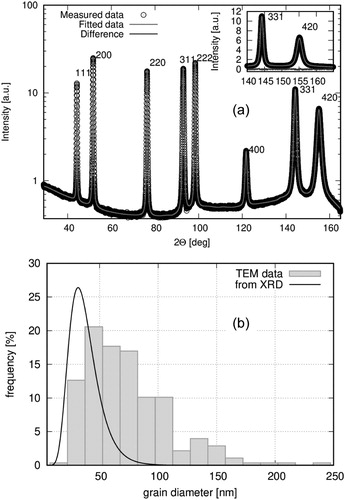
Table 1. Preparation details (electrodeposition bath and substrate), TEM grain size (d), XRD crystallite size (<x>) obtained from the eCMWP analysis and room-temperature resistivity (ρ) of the investigated ED nc-Ni foils.
3.2.3. XRD study of the microstructure of the ED Ni samples #B2 and #Ni(TKE)
In this subsection, we will present the results of the XRD studies on the previously prepared two ED Ni samples, #B2 and #Ni(TKE).
The measured XRD patterns were evaluated both by the eCMWP procedure as for the ED Ni series in Section 3.2.2 and by the modified Williamson-Hall analysis as described in Ref. Citation25 for another ED Ni sample from our laboratory.
The XRD crystallite sizes from the eCMWP procedure were <x> = 66 ± 7 nm (sample #B2) and 57 ± 6 nm (sample Ni(TKE)). By using the modified Williamson-Hall XRD analysis [Citation25], we obtained <x> = 82 ± 9 nm (sample #B2) and 61 ± 7 nm (sample Ni(TKE)). For both samples, <x> is smaller when evaluated by the eCMWP procedure. This is understandable since in this method <x> is defined as the arithmetically averaged grain size, whereas in the modified Williamson-Hall analysis the obtained size parameter <x> corresponds to a volumetrically weighted average of the crystallite sizes and, thus, the larger weighting factor of large crystallites shifts the average upwards. In any case, the XRD data demonstrate that these two ED samples can also be considered as nc-Ni.
Due to the lower thickness of these two deposit samples, their recorded XRD patterns and the evaluated crystallite sizes are characteristic for the total deposit thickness. It is noted furthermore that, in order to keep homogeneity, when displaying the resistivity against XRD crystallite size later, for these two samples we will use only the <x> values derived from the eCMWP analysis.
3.2.4. XRD study of the microstructure of the metallurgically processed Ni sample #B5
The width of the Bragg peaks of sample #B5 was as narrow as the instrumental broadening. Therefore, the diffraction profiles could not be used to deduce the crystallite size of this sample. Nevertheless, according to former investigations [Citation22], such narrow diffraction peaks usually indicate crystallite sizes larger than one micrometer. A comparison of the diffraction profiles of samples #B2 and #B5 also revealed that the crystallite size of sample #B5 is definitely much larger than that of sample #B2. Accordingly, in the following sections sample #B5 will be referred to as microcrystalline Ni (μc-Ni) and it corresponds actually to bulk Ni.
Although no structural study was carried out for the other metallurgically processed Ni foil samples, they should exhibit fairly similar structural features as the bulk Ni sample #B5.
3.3. Electrical transport measurements
For the electrical transport measurements, a rectangular strip of about 1–2 mm wide and about 5–20 mm long was cut from the Ni foils. A four-point-in-line probe with spring contacts was used to measure the resistance of the strips at room temperature.
The resistivity ρ was determined from the usual formula: Rm = ρ·lr/(t·w) where Rm is the measured resistance between the two gold-plated and pin-shaped potential contacts separated by a distance lr, t is the strip thickness and w is the strip width. The strip thickness t was determined from the known density as well as the measured width w and mass m of the strip having a total length of lm. We used 8.91 g/cm3 for the room-temperature density of Ni [Citation26].
The least accurate parameter of the sample dimensions in the above resistivity formula is the foil thickness t which was in the range 5–100 μm. As mentioned above, for getting parameter t, we need to know the strip width w that was determined the following way: by taking a top-view photographic image of the strip, we determined the strip area by an image-processing software, then calculated the average strip width w by using the measured strip length lm. This density-based procedure yielded much less scattered resistivity values than by measuring directly the strip thickness by any mechanical calliper or dial.
4. Resistivity results on bulk and nanocrystalline Ni
4.1. Bulk (microcrystalline) Ni samples
As described in Section 3.1, four different bulk Ni samples were investigated in the present work.
The most detailed measurements were carried out for the Ni sample #B5. Six independent strips with a length of about 20 mm and a width of about 2 mm were cut from the 5–10 mm wide cold-rolled and annealed strips. For each strip used for the resistivity measurement, the thickness was determined by the photographic method described in Section 3.3. Then, the resistance was measured for each strip 5–6 times to get their average resistance individually which were then converted to get their resistivity ρ. Finally, the ρ values were averaged and this yielded the following average resistivity for the Ni sample #B5: ρ = 7.36 μΩ·cm with a standard deviation of ±0.21 μΩ·cm. The latter value represents an error of ±3 % for the average value of resistivity. This can be considered as the accuracy of the resistivity determination by our measurement method for the sample dimensions and resistivities studied here.
The standard room-temperature resistivity value for bulk Ni is ρ = 7.24 μΩ·cm [Citation27]. This means that with our experimental procedure we could reproduce the pure Ni reference value on our strip samples with the sizes used within our experimental uncertainty.
The resistivity values were determined also for the other three bulk (microcrystalline) Ni samples, for each sample on a single strip and the results obtained are as follows: (i) ρ = 7.32 μΩ·cm for sample #GF-Ni(50 μm), (ii) ρ = 7.35 μΩ·cm for sample #GF-Ni(250 μm) and ρ = 7.54 μΩ·cm for sample #Ni(99.99+%). It can be seen that for the first two samples the ρ values are also very close to the standard bulk Ni value, they are within the same error range (±3 % ) as sample #B5 and even for the third sample (#Ni(99.99+%)), the deviation is still within 4 %.
4.2. Nanocrystalline Ni samples
The resistivity was measured in detail for the samples of the ED Ni series. For one strip of each sample, the resistance was measured seven times and averaged to get the resistivity values of each sample. For four of the ED Ni series samples, two more strips were also measured in the same way and, finally, all the resistivity data of a given sample were averaged.
summarises the preparation details, the grain size d from TEM and the crystallite size <x> from XRD line profile analysis for the investigated ED nc-Ni samples. From most of the bath types, two nominally identical samples were prepared, one on Cu and another one on steel substrates. As explained in Section 3.2, the structural data were taken either from Ref. Citation17 or were obtained in the present study as indicated in the sixth column of .
The grain size values were obtained by a weighted average of the TEM data for the planar and cross-sectional measurements, for the latter including both the substrate and electrolyte sides of the deposits. The crystallite sizes given were obtained as the averages of the XRD data measured on both sides of the deposits (the XRD study was performed only on nc-Ni samples which were prepared on Cu substrate). It appears that the XRD crystallite sizes are typically well below the TEM grain sizes. The major reason for the difference is that, as explained in detail in Refs. Citation16 and Citation17, XRD measures the size of the coherently scattering regions (crystallites) and this is usually below the grain diameter that one can directly assess from the TEM images. A comparison of the TEM grain sizes and the XRD crystallite sizes on the very same ED nc-Ni samples in Ref. Citation17 revealed that the smaller the TEM grain size, the closer is the XRD crystallite size to it, with the two quantities becoming equal around 17 nm grain size. The new results presented in (b) give further support for this former conclusion.
The room-temperature resistivity data on the samples of the ED Ni series are given in the last column of . As noted in Section 3.1, two samples of this series were found to contain Co impurity, specifically sample #TN2 contained 2.9 at.% Co and sample #NC*33 contained 3.6 at.% Co. According to Ref. Citation28, the residual resistivity increase in Ni is 0.16 μΩ·cm/at.% Co impurity. By using this value, we can estimate that for these two Ni samples, from the measured resistivity as given in the last column of , about 0.5 μΩ·cm is due to the presence of the Co impurity atoms. By subtracting this contribution, the resulting room-temperature resistivity is given in italics in bracket after the measured value for these two samples. So these bracketed resistivity data can be considered as the correct values for the resistivity of pure nc-Ni with the specified grain size.
The ρ value was determined also for the other two ED Ni samples and the results were as follows: (i) ρ = 9.96 μΩ·cm for #Ni(TKE) and (ii) ρ = 8.78 μΩ·cm for #B2.
It is clear that all the resistivity data on our nc-Ni foils are larger than the bulk (microcrystalline) Ni value ρbulk = 7.24 μΩcm [Citation27]. According to the data in , obviously, the trend is that the smaller the grain size, the larger the resistivity. The observed trend is in line with expectation based on the increasing amount of grain boundaries with decreasing grain size, which represent excess scattering centres for the conduction electrons, leading finally to an increase of the electrical resistivity [Citation1,Citation13,Citation14,Citation29].
5. Specific grain-boundary resistivity of Ni
5.1. Analysis on the basis of all resistivity data reported for nc-Ni metal
5.1.1. Resistivity vs. TEM gain size d
The observed trend of the evolution of the room-temperature resistivity with grain size in our nc-Ni samples is in good agreement with the results of all previous investigations on electrodeposited nc-Ni [Citation12–15,Citation21,Citation30–32]. shows all available resistivity vs. TEM grain size data reported on electrodeposited nc-Ni, including the present results. When fitting all available data to eq. (5) with fixed ρbulk = 7.24 μΩ·cm [Citation27], the thick solid line was obtained with a reasonably high fit quality (R2 = 0.80) and with the Andrews parameter A = 14.7·10−16 Ω·m2. We have performed the fit for all the TEM data also by allowing ρbulk to vary: the values of A and ρbulk changed by about 6 % only whereas the fit quality parameter R2 improved by less than 1 % only. Therefore, we will retain the fixed ρbulk = 7.24 μΩ·cm value for the fit and thus consider the resulting A(Ni,300K) = 14.7·10−16 Ω·m2 value as the best fit result from the resistivity vs. TEM grain size data reported for all electrodeposited nc-Ni samples.
Figure 3. Room-temperature resistivity ρ for all electrodeposited nc-Ni samples as a function of the TEM grain size d. Key to symbols: open circles (present data on the ED Ni series from ); open triangles (data from our previous works [21,30,31]); open squares [Citation13] and open diamonds [Citation32]. The thick solid line represents a fit to eq. (5) for all displayed TEM data with fixed ρbulk = 7.24 μΩcm and with the fitted value A = 14.7·10−16 Ωm2 (fit quality: R2 = 0.80).
![Figure 3. Room-temperature resistivity ρ for all electrodeposited nc-Ni samples as a function of the TEM grain size d. Key to symbols: open circles (present data on the ED Ni series from Table 1); open triangles (data from our previous works [21,30,31]); open squares [Citation13] and open diamonds [Citation32]. The thick solid line represents a fit to eq. (5) for all displayed TEM data with fixed ρbulk = 7.24 μΩcm and with the fitted value A = 14.7·10−16 Ωm2 (fit quality: R2 = 0.80).](/cms/asset/e30286db-f214-4dc5-a0ad-08731cabcba3/tphm_a_1580399_f0003_ob.jpg)
It is noted that for samples #TN2 and #NC*33 in , we used in (and later also in ) the resistivity values obtained after correcting for the Co impurity content. However, even when using the original measured resistivity values, the Andrews parameter from the fit of the data to eq. (5) changes in the fourth digit only (by about 0.3 %), so the above A(Ni,300K) = 14.7·10−16 Ω·m2 value pertains for Ni for both resistivity values of samples #TN2 and #NC*33.
Figure 4. Room-temperature resistivity ρ for electrodeposited nc-Ni samples as a function of the XRD crystallite size <x>. Key to symbols: closed circles: present data on the ED Ni series from and on samples #B2 and #Ni(TKE); closed triangles [Citation14]; solid squares [Citation15]. The thick solid line is identical with that of (ρ vs. TEM grain size, from fit for all TEM-based data); the dash-dot line represents an approximate average over all displayed XRD data.
![Figure 4. Room-temperature resistivity ρ for electrodeposited nc-Ni samples as a function of the XRD crystallite size <x>. Key to symbols: closed circles: present data on the ED Ni series from Table 1 and on samples #B2 and #Ni(TKE); closed triangles [Citation14]; solid squares [Citation15]. The thick solid line is identical with that of Figure 4 (ρ vs. TEM grain size, from fit for all TEM-based data); the dash-dot line represents an approximate average over all displayed XRD data.](/cms/asset/da98f0ec-13e1-4afb-9ea5-589665a2256a/tphm_a_1580399_f0004_ob.jpg)
5.1.2. Resistivity vs. XRD crystallite size <x>
As a next step, we will consider the resistivity data vs. XRD crystallite size <x> for electrodeposited nc-Ni. shows the results from the three studies where such data are available (this work as well as Refs. Citation14 and Citation15). For comparison, we have added to also the fit result (thick solid line) for all TEM data from . As explained beforehand (and can also be seen for our ED Ni series samples in ), the XRD crystallite size <x> for a given sample is always smaller than the TEM grain size d. Clearly, whereas the available TEM-based results were scattered more or less uniformly around the ‘all-TEM’ thick line in , all but one of the XRD-based data points lie below this reference line in .
The (red) triangles in are the reported data of McCrea et al. [Citation14] which they fitted to eq. (5) with fixed ρbulk = 8.33 μΩ·cm and this yielded then ρSGBR(Ni) = 2.74·10−16 Ω·m2 (by using their kGB = 2.37 value, this corresponds to A = 6.48·10−16 Ω·m2). These authors used the measured resistivity of an annealed ED Ni sample with 300 μm grain size as the fixed ρbulk = 8.33 μΩ·cm value. If we fit the data of McCrea et al. [Citation14] with fixed ρbulk = 7.24 μΩ·cm corresponding to the true bulk resistivity of Ni [Citation27], we get A = 8.9·10−16 Ω·m2. By considering the positions of our XRD-based data in (blue dots) with respect to the data points by McCrea et al. [Citation14], one can judge that our data would yield a very similar A value as theirs. The data of Madduri and Kaul [Citation15] displayed in by (black) solid squares would yield somewhat lower A values. Whereas each individual XRD-based datasets in could be fitted to eq. (5) with an acceptable fit quality parameter, the three datasets together show such a large scatter that it is not reasonable to carry out a fit to derive an A value. Therefore, we have just indicated by the dash-dot line in an approximate average over all XRD-based data which would correspond to an A value about half that derived from the TEM-based data in .
It should be noted at this point that the large discrepancy between the results of various XRD-based studies may partly come from the fact that different evaluation procedures of the XRD pattern usually lead to different crystallite size data as discussed at the beginning of Section 3.2. In Section 3.2.3, we have provided results that support this statement. Furthermore, a look at the XRD data evaluation plots of an earlier ED Ni sample in Figs. 1 and 2 of Ref. Citation25 immediately reveals that the Scherrer formula, the classical and modified Williamson-Hall analysis all will lead to different <x> values. McCrea et al. [Citation14] used the Scherrer formula to derive the crystallite size, while in Section 3.2 we applied the XRD eCMWP procedure for all of our ED Ni samples or constructed the modified Williamson-Hall plot (for samples #B2 and #Ni(TKE)). At the same time, Madduri and Kaul [Citation15] used yet another method (the so-called Halder-Wagner approach [Citation33]) described in more detail in Ref. Citation34. Since each of the XRD evaluation methods accounts differently for the influence of various lattice defects on line broadening and, furthermore, because the details of the electrodeposition procedure determine the types and amount of lattice defects, the different XRD evaluation methods of differently prepared samples may easily lead to the observed large differences in the resistivity data when displaying the results of various reports as a function of the XRD crystallite size. A further reason for discrepancy may come from different XRD measurement arrangements as well since, depending on whether the detector scans an angular range or the sample is rotated, the grain size evaluated from the XRD line broadening may yield a value either along the normal of the foil plane or along a different angle.
In spite of all these uncertainties, we can conclude that an evaluation of the resistivity data on the basis of the available XRD crystallite sizes results in an A value by about a factor of two smaller than an evaluation on the basis of the TEM grain sizes, the latter yielding a room-temperature value of A(Ni) = 14.7·10−16 Ω·m2. The reason for the discrepancy between the XRD-based and TEM-based evaluation lies in the fact that TEM yields larger grain sizes than the crystallite size provided by XRD for the same sample [Citation16,Citation17] as evidenced also in for our ED Ni series. This is because within the grains, lattice defects such as dislocation walls, stacking and twin faults are frequently observed by TEM [Citation16] which break the coherency of the scattering of X-rays and, thus, cause a line broadening resulting in a smaller XRD crystallite size than the TEM grain size. On the other hand, the contribution of these coherency-breaking defects to the resistivity is much smaller than that of the grain boundaries as was demonstrated both experimentally [Citation4,Citation35] and theoretically [Citation11]. Therefore, the grain size derived from TEM should be considered as the relevant parameter when accounting for the specific grain-boundary resistivity.
Based on all this, we conclude that our A(Ni) = 14.7·10−16 Ω·m2 parameter obtained from all TEM-based resistivity data provides a reliable representation of the grain-boundary contribution to the resistivity of Ni metal. The conversion of our A(Ni) value to ρSGBR(Ni) will be made later when comparing the experimental data to the theoretical values.
5.2. Comments on earlier resistivity results on nanophase Ni
There are also resistivity data reported for thin Ni films which are certainly fine-grained and often even nanocrystalline. This is because it is well-known that for sufficiently thin films produced with any atom-by-atom deposition process, the deposit grain size can decrease down to the nanosized regime, the lateral grain size being typically very close to the film thickness. In addition, very small film thicknesses may also result in an excess resistivity contribution due to the enhanced surface scattering term [Citation36–41]. The room-temperature resistivity data of Reale [Citation42] on thin Ni films and the corresponding data of Böhnert et al. [Citation43] for Ni nanowires demonstrate that the combined effect of a nanocrystalline structure and the confined sample geometry can lead to much larger resistivities than the bulk value. Unfortunately, at film thicknesses which are comparable to the electronic mean free path, the grain-boundary and surface scattering contributions to the resistivity are hard to separate from each other [Citation38–40].
At this point, it is appropriate to make a note on the frequently quoted [Citation2,Citation7,Citation10] specific grain-boundary resistivity value derived from the room-temperature experimental resistivity data of Wissmann [Citation44] on evaporated Ni films. Wissmann [Citation44] studied the microstructure of the Ni films by XRD to determine the crystallite size <x> and displayed the data as ρ·<x> vs. <x> which yielded a fairly linear plot. Fitting a straight line to these data yielded parameters which can be converted into a relation corresponding to eq. (5): ρ = 12 μΩ·cm + A/<x> with A(Ni) = 28.8·10−16 Ω·m2. Apparently, this A value was used by Lormand [Citation2] in his as the specific grain-boundary resistivity for Ni which is evidently wrong by a factor of about 3 (the magnitude of kGB). Brown [Citation7] quoted ρSGBR(Ni) = 14·10−16 Ω·m2 from the results of Wissmann [Citation44] which is also too large in view of our results on the basis of the XRD crystallite sizes. The A(Ni) value from the data of Wissmann [Citation44] is higher than our value by a factor of two with respect to the TEM-based data or by a factor of four with respect to the XRD-based data. The reason for the much higher value of A for the samples of Wissmann [Citation44] comes partly from the fact that the bulk Ni resistivity value of ρbulk = 12 μΩ·cm deduced from his samples is also well above the true bulk Ni value of ρbulk = 7.24 μΩ·cm [Citation27]. In line with this, it should be mentioned that the resistivity of a Ni film with 10 nm thickness is about twice as high in Wissmann’s work [Citation44] than the value reported by Reale [Citation42] for the same thickness. The fact that the resistivity values of the Ni films of Wissmann [Citation44] are too large is shown by calculating the resistivity of a film with a crystallite size of 100 nm. Using A(Ni) = 28.8·10−16 Ω·m2 and ρbulk = 12 μΩ·cm, we get about 15 μΩ·cm for such a film. Including this value in the plot of immediately reveals that it is much higher than the presently discussed nc-Ni resistivity values for comparable grain sizes. It is not clear what is the origin of the too high resistivities of the Ni films of Wissmann [Citation44], but an increased surface roughness or an eventual contamination/oxidation of the films may have easily resulted in the excess resistivity reported. In any case, the present results for Ni suggest that the A and ρSGBR data derived from the results of Wissmann [Citation44] and quoted in Refs. Citation2, Citation7 and Citation10 are definitely too large and do not represent the true values for pure Ni.
5.3. Comparison of experimental and theoretical ρSGBR data for Ni
As discussed at the end of Section 2, due to the uncertainty of the proportionality factor kGB, a comparison of the grain-boundary contribution to the resistivity should be made on the basis of the experimentally directly determined Andrews parameter A.
In Section 5.1, from an analysis of all available resistivity data on nc-Ni samples for which TEM grain size data were reported, we obtained A(Ni,300K) = 14.7·10−16 Ω·m2.
The most recent calculation for the specific grain-boundary resistivity of Ni metal has been reported by Karolik and Luhvich [Citation10] whose result was ρSGBR(Ni) = 6.2·10−16 Ω·m2 whereas a previous calculation [Citation7] provided ρSGBR(Ni) = 1.9·10−16 Ω·m2. Above, we have derived A(Ni,300K) = 14.7·10−16 Ω·m2 for the Andrews parameter from the experimental data on Ni and we should consider the relation A = kGB·ρSGBR to make a conversion. As outlined in Section 2, the value of kGB can vary from 2.37 to 3.24 in the various considerations. Accordingly, the specific grain-boundary resistivity of Ni from our evaluation of the nc-Ni data at room temperature can be in the range 4.45·10−16 Ω·m2 < ρSGBR(Ni) < 6.2·10−16 Ω·m2. Our upper bound matches very well the calculated value of Karolik and Luhvich [Citation10] whereas the previous theoretical result of Brown [Citation7] is outside the experimental range defined by the uncertainty of kGB.
5.4. Resistivity of nc-Ni for very small grain sizes: comparison with amorphous Ni
According to the TEM selected-area diffraction patterns reported in Refs. Citation16 and Citation17, electrodeposited nc-Ni samples such as those investigated in the present work exhibit a fairly uniformly random orientation of the crystallites. Therefore, evidently, the deduced grain-boundary resistivity values represent an average over all type of grain boundaries which occur in these samples. On the other hand, with decreasing grain size, the grain-boundary contribution to the measured resistivity increases. As demonstrates, for grain sizes around 10 nm the room-temperature resistivity of nc-Ni can be as high as three times the bulk value.
The increasing volume fraction of grain boundaries with decreasing grain size implies that a larger and larger fraction of atoms is in a topological state deviating from the perfect crystal. We may, therefore, ask how high the resistivity of nc-Ni can be if the grain size is reduced to the extreme where the majority of atoms is situated in a position not corresponding to a site within a perfect crystal of Ni.
An upper limit for the resistivity of Ni can be set as the resistivity of the structurally most disordered, i.e. amorphous state. Since Ni metal has not yet been produced in amorphous state, we can attempt to estimate the resistivity of amorphous Ni from the data on the resistivity of liquid Ni [Citation45–48]. shows the temperature dependence of the resistivity of Ni in the solid state [Citation27] and in the liquid state [Citation45]. It can be seen that at high temperatures the resistivity of the solid fcc phase increases slowly up to the melting point Tm. At the melting temperature, the resistivity suddenly jumps from about 55 μΩ·cm of the solid fcc phase to about 85 μΩ·cm of the liquid state, the latter exhibiting a complete topological disorder. The thin solid line above Tm represents the resistivity evolution with temperature in the liquid state as reported in Ref. Citation45. Similar temperature dependence of the resistivity was observed for liquid Ni also in Refs. Citation46–48 and the two dashed lines as well as the two dash-dot lines represent the extrapolation of the liquid-state resistivity data of all these works to room temperature. Since the liquid and amorphous state can be considered as having the same disordered topological arrangement of Ni atoms, we can consider the liquid-state resistivity extrapolated to 300 K as corresponding approximately to the room-temperature resistivity of amorphous Ni. According to , the resistivity of amorphous (a) Ni at T = 300 K can be taken as about ρ(a-Ni) = 70 ± 10 μΩ.cm.
Figure 5. Temperature dependence of the resistivity ρ of Ni metal in the solid fcc phase [Citation27] and in the liquid state as well as the extrapolation of the liquid-state data to 300 K from Refs. Citation45–48. Tc: Curie point; Tm: melting point.
![Figure 5. Temperature dependence of the resistivity ρ of Ni metal in the solid fcc phase [Citation27] and in the liquid state as well as the extrapolation of the liquid-state data to 300 K from Refs. Citation45–48. Tc: Curie point; Tm: melting point.](/cms/asset/b05d3a81-7894-4121-8059-a190c3ac3279/tphm_a_1580399_f0005_ob.jpg)
By inserting now the experimentally derived Andrews parameter A(Ni,300K) = 14.7·10−16 Ω·m2 into eq. (5) with ρbulk = 7.24 μΩ·cm [Citation27], we can estimate that the resistivity of nanocrystalline Ni reaches the above value for amorphous Ni at a grain size of d = 2.3 ± 0.4 nm.
On the other hand, by assuming a grain boundary thickness of 1 nm, Palumbo et al. [Citation49] estimated that at this grain size the fraction of atoms within the crystallites reduces to about 20 % whereas the fraction of atoms in both the grain boundaries and in the triple line junctions between three connecting grains amounts to about 40 %. This implies that at a grain size of about 2.3 nm, most of the atoms are already situated in a topologically rather disordered state, so the whole nanocrystalline material has an atomic disorder certainly very close to that of the amorphous state. This supports the above conclusion that at this small grain size the resistivity of nc-Ni matches fairly well that of amorphous Ni.
6. Summary
In the present paper, the main emphasis was put on analysing the grain size dependence of the electrical resistivity in metals in order to extract the specific grain-boundary resistivity (ρSGBR). We have relied on the original analysis procedure of Andrews [Citation3] who recognised that the contribution of the grain boundaries (ρGB) to the total resistivity increases linearly with the grain-boundary surface area per unit volume (SGB/V) and, thus, ρGB = ρSGBR·(SGB/V). On the other hand, topological considerations lead to the result that SGB/V = kGB (1/d) where d is the average grain diameter and kGB is a model-dependent proportionality constant varying in the reported cases from 2.37 to 3.24. Along this line, we can write for the total resistivity ρ = ρbulk + ρGB = ρbulk + A/d where the Andrews parameter A = ρSGBR·kGB is introduced. Due to the large variation of the kGB factor in various models, it is suggested to compare results of various reports on a given metal on the basis of the A parameter rather than the ρSGBR values which may depend on the actual choice of the kGB factor. The same is true if we want to compare specific grain-boundary resistivity data for two different metals or experimental and theoretical data for a given metal.
We have presented new results for the room temperature electrical resistivity of nc-Ni by measurements on electrodeposited Ni foils for which the structural characterisation included both the grain sizes d determined by TEM and the crystallite sizes <x> deduced from XRD analysis. Based on these structural data, we compared our results with previously reported nc-Ni resistivity data. The data from all measurements could be properly analysed according to the procedure of Andrews [Citation3]. However, it could be established that we get different A values when analysing the data for samples for which the TEM grain size was reported and data for samples with XRD crystallite sizes. The systematic difference is explained with the help of our ED Ni series samples for which both d and <x> data were available and the difference could be traced back to the different meaning of the two kinds of structural parameter. The structural parameter relevant for the electrical resistivity is the TEM grain size d since the XRD crystallite size <x> involves also the effect of coherency-breaking lattice defects inside the grains which, on the other hand, give a negligible contribution only to the resistivity [Citation4,Citation11,Citation35].
Based on the above considerations, we could deduce A(Ni) = 14.7·10−16 Ω·m2 at room temperature by taking into account all available resistivity results where TEM grain sizes were reported. By considering the uncertainty of the kGB factor, this can be converted to a range of ρSGBR(Ni) values. The specific grain-boundary resistivity of Ni from our evaluation of all nc-Ni resistivity data at room temperature is in the range 4.45·10−16 Ω·m2 < ρSGBR(Ni) < 6.2·10−16 Ω·m2 and our upper bound agrees exactly with the most recent theoretical value in the literature [Citation10]. By using the ρSGBR(Cu) value reported by Andrews et al. [Citation3,Citation4], we find that ρSGBR(Ni) ∼ 2 ρSGBR(Cu) which is in good qualitative agreement with the ratio of the resistivities of bulk of Ni and Cu.
By using the experimentally determined Andrews parameter for Ni, we have estimated that the resistivity of nc-Ni reaches the resistivity of amorphous Ni at a grain size of about 2.3 nm where most of the atoms are already situated in topologically rather disordered sites strongly resembling the amorphous state. This finding also justifies the reliability of the analysis on the basis of eq. (5) since an extrapolation from the grain size range where resistivity data were available down to extremely small grain sizes yields a resistivity value in reasonable agreement with the estimated room-temperature resistivity of amorphous Ni. This latter value can be considered as an upper limit for the room-temperature resistivity of Ni metal, i.e. the resistivity of nc-Ni should have a saturation around grain sizes as small as 2–3 nm.
Acknowledgements
Work in Budapest was supported by the Research Group Linkage Programme (Project Ref. 3.4 – 1001292 – HUN - IP) of the Alexander von Humboldt Foundation, Germany with the funding provided by the Federal Ministry of Education and Research, Germany. This research was carried out also in the framework of the COST Action MP1407. The comments of L.F. Kiss during the final shaping of the manuscript are gratefully acknowledged.
Disclosure statement
No potential conflict of interest was reported by the authors.
ORCID
I. Bakonyi http://orcid.org/0000-0002-5873-8601
Additional information
Funding
References
- J.M. Ziman, Electrons and Phonons, Clarendon Press, Oxford, 1960. Ch. VI.
- G. Lormand, Electrical properties of grain boundaries. J. Phys. Coll. 43 (1982), pp. C6/283–C6/292.
- P.V. Andrews, Resistivity due to grain boundaries in pure copper. Phys. Lett 19 (1965), pp. 558–560. doi: 10.1016/0031-9163(65)90776-6
- P.V. Andrews, M.B. West and C.R. Robeson, The effect of grain boundaries on the electrical resistivity of polycrystalline copper and aluminium. Philos. Mag 19 (1969), pp. 887–898. doi: 10.1080/14786436908225855
- M.B. Kasen, Grain boundary resistivity of aluminium. Philos. Mag 21 (1970), pp. 599–610. doi: 10.1080/14786437008238442
- K.M. Mannan and K.R. Karim, Grain boundary contribution to the electrical conductivity of polycrystalline Cu films. J. Phys. F 5 (1975), pp. 1687–1693. doi: 10.1088/0305-4608/5/9/009
- R.A. Brown, Electrical resistivity of dislocations in metals. J. Phys. F 7 (1977), pp. 1477–1488. doi: 10.1088/0305-4608/7/8/015
- G. Lormand and M. Chevreton, Theoretical determination of the resistivity of relaxed periodic grain boundaries. Application to (112) twin boundaries in normal body-centred-cubic metals. Philos. Mag. B 44 (1981), pp. 389–404. In French. doi: 10.1080/01418638108223561
- I. Nakamichi, Electrical resistivity and grain boundaries in metals. Mater. Sci. Forum 207-209 (1996), pp. 47–58. and references therein. doi: 10.4028/www.scientific.net/MSF.207-209.47
- A.S. Karolik and A.A. Luhvich, Calculation of electrical resistivity produced by dislocations and grain boundaries in metals. J. Phys.: Cond. Matter 6 (1994), pp. 873–886.
- M. César, D.P. Liu, D. Gall and H. Guo, Calculated resistances of single grain boundaries in copper. Phys. Rev. Appl 2 (2014), pp. 044007/1–11. doi: 10.1103/PhysRevApplied.2.044007
- I. Bakonyi, E. Tóth-Kádár, T. Tarnóczi, L.K. Varga, Á Cziráki, L. Gerőcs and B. Fogarassy, Structure and properties of fine-grained electrodeposited nickel. Nanostruct. Mater 3 (1993), pp. 155–161. doi: 10.1016/0965-9773(93)90073-K
- M.J. Aus, B. Szpunar, U. Erb, A.M. El-Sherik, G. Palumbo and K.T. Aust, Electrical resistivity of bulk nanocrystalline nickel. J. Appl. Phys 75 (1994), pp. 3632–3634. doi: 10.1063/1.356076
- J.L. McCrea, K.T. Aust, G. Palumbo and U. Erb, Electrical resistivity as a characterization tool for nanocrystalline metals. MRS Symp. Proc. 581 (2000), pp. 461–466. J.L. McCrea, Ph.D. Thesis, University of Toronto, Canada, 2001. doi: 10.1557/PROC-581-461
- P.V.P. Madduri and S.N. Kaul, Magnon-induced interband spin-flip scattering contribution to resistivity and magnetoresistance in a nanocrystalline itinerant-electron ferromagnet: effect of crystallite size. Phys. Rev. B 95 (2017), pp. 184402/1–12. doi: 10.1103/PhysRevB.95.184402
- T. Kolonits, P. Jenei, B.G. Tóth, Z. Czigány, J. Gubicza, L. Péter and I. Bakonyi, Characterization of defect structure in electrodeposited nanocrystalline Ni films. J. Electrochem. Soc 163 (2016), pp. D107–D114. doi: 10.1149/2.0911603jes
- T. Kolonits, P. Jenei, L. Péter, I. Bakonyi, Z. Czigány and J. Gubicza, Effect of bath additives on the microstructure, lattice defect density and hardness of electrodeposited nanocrystalline Ni films. Surf. Coat. Technol 349 (2018), pp. 611–621. doi: 10.1016/j.surfcoat.2018.06.052
- R.T. DeHoff and F. Rhines, Quantitative Microscopy, McGraw-Hill, New York, 1968.
- C.S. Smith and L. Guttman, Measurement of internal boundaries in three-dimensional structures by random sectioning. J. Metals 5 (1953), pp. 81–87.
- J.H. Hensler, The relation between grain section and grain size. J. Inst. Metals 96 (1968), pp. 190–192.
- I. Bakonyi, E. Tóth-Kádár, L. Pogány, Á Cziráki, I. Gerőcs, K. Varga-Josepovits, B. Arnold and K. Wetzig, Preparation and characterization of DC plated nanocrystalline nickel electrodeposits. Surf. Coat. Technol 78 (1996), pp. 124–136. doi: 10.1016/0257-8972(94)02399-9
- J. Gubicza, X-ray Line Profile Analysis in Materials Science, IGI-Global, Hershey, PA, 2014. ISBN: 978-1-4666-5852-3.
- B.D. Cullity and S.R. Stock, Elements of X-ray Diffraction, 3rd ed., Prentice Hall, Upper Saddle River, New Jersey, 2001.
- T. Ungár and A. Borbély, The effect of dislocation contrast on x-ray line broadening: A new approach to line profile analysis. Appl. Phys. Lett 69 (1996), pp. 3173–3175. doi: 10.1063/1.117951
- T. Ungár, Á Révész and A. Borbély, Dislocations and grain size in electrodeposited nanocrystalline Ni determined by the modified Williamson-Hall and Warren-Averbach procedures. J. Appl. Cryst 31 (1999), pp. 554–558. doi: 10.1107/S0021889897019559
- C. Kittel, Introduction to Solid State Physics, 6th ed., Wiley, New York, 1986.
- M.J. Laubitz, T. Matsumura and P.J. Kelly, Transport properties of the ferromagnetic metals. II. Nickel. Can. J. Phys. 54 (1976), pp. 92–102. quoted as reference data by J. Bass, Chapter 1: Electrical resistivity of pure metals and dilute alloys, in Landolt-Börnstein - Group III, New Series, Springer-Verlag, Berlin, Heidelberg, New York, 1982, Vol. 15a, pp. 1–287. doi: 10.1139/p76-011
- I.A. Campbell, A. Fert, Transport properties of Ferromagnets, in Ferromagnetic Materials, Vol. 3, Ch. 9, Wohlfarth E.P., eds., North-Holland, Amsterdam, 1982. pp. 747–804.
- I. Bakonyi, E. Tóth-Kádár, J. Tóth, Á Cziráki and B. Fogarassy, Electronic transport in nanocrystalline metals: a study of electrodeposited nickel foils, in Nanophase Materials. NATO ASI Series E, Vol. 260, G.C. Hadjipanayis, R.W. Siegel, eds., Kluwer Academic Publishers, Dordrecht, The Netherlands, 1994. pp. 423–432.
- I. Bakonyi, B. Pula, E. Tóth-Kádár, I. Gerőcs and Á Cziráki, (unpublished); B. Pula, M.Sc. Thesis, Eötvös University, Budapest, Hungary, 1996.
- E. Tóth-Kádár, I. Bakonyi, L. Pogány and Á Cziráki, Microstructure and electrical transport properties of pulse plated nanocrystalline nickel electrodeposits. Surf. Coat. Technol 88 (1997), pp. 57–65. doi: 10.1016/S0257-8972(96)02896-4
- H.J. Cho, S. Wang, Y. Zhou, G. Palumbo and U. Erb, Thermal conductivity of bulk electrodeposited nanocrystalline nickel. Int. J. Heat Mass Transf 100 (2016), pp. 490–496. doi: 10.1016/j.ijheatmasstransfer.2016.04.068
- N.C. Halder and C.N.J. Wagner, Separation of particle size and lattice strain in integral breadth measurements. Acta Cryst 20 (1966), pp. 312–313. doi: 10.1107/S0365110X66000628
- P.V.P. Madduri and S.N. Kaul, Core and surface/interface magnetic anisotropies in nanocrystalline nickel. J. All. Comp 689 (2016), pp. 533–541. doi: 10.1016/j.jallcom.2016.07.256
- L. Lu, Y. Shen, X. Chen, L. Qian and K. Lu, Ultrahigh strength and high electrical conductivity in copper. Science 304 (2004), pp. 422–426. doi: 10.1126/science.1092905
- K. Fuchs, The conductivity of thin metallic films according to the electron theory of metals. Proc. Cambr. Philos. Soc 34 (1938), pp. 100–108. doi: 10.1017/S0305004100019952
- E.H. Sondheimer, The mean free path of electrons in metals. Adv. Phys 1 (1952), pp. 1–42. doi: 10.1080/00018735200101151
- J.R. Sambles, The resistivity of thin metal films – some critical remarks. Thin Solid Films 106 (1983), pp. 321–331. doi: 10.1016/0040-6090(83)90344-9
- J. Vancea, G. Reiss and H. Hoffmann, Mean-free-path concept in polycrystalline metals. Phys. Rev. B 35 (1987), pp. 6435–6437. doi: 10.1103/PhysRevB.35.6435
- J. Vancea, Unconventional features of free electrons in polycrystalline metal films. Int. J. Mod. Phys. B 3 (1989), pp. 1455–1501. doi: 10.1142/S0217979289000956
- R. Henriquez, S. Cancino, A. Espinosa, M. Flores, T. Hoffmann, G. Kremer, J.G. Lisoni, L. Moraga, R. Morales, S. Oyarzun, M.A. Suarez, A. Zúñiga and R.C. Munoz, Electron grain boundary scattering and the resistivity of nanometric metallic structures. Phys. Rev. B 82 (2010), pp. 113409/1–4. doi: 10.1103/PhysRevB.82.113409
- C. Reale, Electrical properties of vacuum deposited nickel films. Phys. Lett A 24 (1967), pp. 145–146. doi: 10.1016/0375-9601(67)90732-3
- T. Böhnert, V. Vega, A.K. Michel, V.M. Prida and K. Nielsch, Magneto-thermopower and magnetoresistance of single Co-Ni alloy nanowires. Appl. Phys. Lett 103 (2013), pp. 092407/1–5. doi: 10.1063/1.4819949
- P. Wissmann, On the influence of the polycrystalline structure on the electrical resistivity of evaporated nickel films. Thin Solid Films 5 (1970), pp. 329–338. In German. doi: 10.1016/0040-6090(70)90105-7
- H.-J. Güntherodt, E. Hauser, H.U. Künzi and R. Müller, The electrical resistivity of liquid Fe, Co, Ni and Pd. Phys. Lett. A 54 (1975), pp. 291–292. doi: 10.1016/0375-9601(75)90263-7
- U. Seydel, W. Fucke and B. Möller, The electrical resistivity of exploding Ni-wires in fast RCL-circuits. Z. Naturf 32a (1977), pp. 147–151.
- Y. Kita and Z. Morita, The electrical resistivity of liquid Fe-Ni, Fe-Co and Ni-Co alloys. J. Non-Cryst.-Sol 61-62 (1984), pp. 1079–1084. doi: 10.1016/0022-3093(84)90684-7
- G. Pottlacher, H. Jäger and T. Neger, Thermophysical measurements on liquid iron and nickel. High Temp. - High Press 19 (1987), pp. 19–27.
- G. Palumbo, S.J. Thorpe and K.T. Aust, On the contribution of triple junctions to the structure and properties of nanocrystalline materials. Scripta Met. Mater 24 (1990), pp. 1347–1350. doi: 10.1016/0956-716X(90)90354-J