
 ?Mathematical formulae have been encoded as MathML and are displayed in this HTML version using MathJax in order to improve their display. Uncheck the box to turn MathJax off. This feature requires Javascript. Click on a formula to zoom.
ABSTRACT
Single-crystalline cast aluminium microwires with a diameter near 15 are characterised by Laue microdiffraction. A microwire in the as-cast condition exhibits a misorientation below
over a length of 500
. The measured density of geometrically necessary dislocations is low,
m−2, though local maxima up to one order of magnitude higher are found. After tensile deformation to failure, the dislocation density is significantly increased in microwires that have mostly deformed in single slip (
m−2), and yet higher when deformation has occurred by multiple slip (
m−2). In deformed single slip oriented microwires, the streaking directions of Laue spots show that dislocations are stored (though not exclusively) on the primary slip system. Results are consistent with a deformation mechanism governed by rotating, likely single-arm, sources.
1. Introduction
Plastic deformation in small-scale metallic samples often differs from what is observed in bulk, macroscopic samples of the same metal or alloy. Generally, it is found that, as the sample size decreases, the plastic flow stress increases, and deformation proceeds in a more irregular, at times stochastic burst-like, manner. The observed behaviour depends on a number of factors, including both the nature of the material, how it was produced, its geometry and the sample size. Recent reviews of the extensive work on the subject can be found in [Citation1–6].
It was shown in a recent publication that single-crystalline net-shape Al microwires, with a diameter in the range of 7–100 , can be produced by a new microcasting process [Citation7]. As compared to other methods used for the fabrication of microtest specimens, specific characteristics of the microcast wires are that they are generally single-crystalline and free of the artefacts that are introduced by other preparation methods such as ion-milling. Cast microwires also have a low initial dislocation density, and their high aspect ratio (
50) makes them suitable for tensile testing. As is reported in [Citation7], these microcast crystals show a size effect in plasticity. This is seemingly because the small size of the crystals leads to source truncation, that is, typical double-pinned Frank–Read sources becoming single-ended (spiral) sources with higher activation stress, as predicted by statistical models [Citation8] and dislocation dynamics simulations [Citation9,Citation10], and evidenced by [Citation11–13] in another class of microcrystals extracted from solidified specimens.
The initial dislocation distribution in such microcrystals, and its evolution during deformation, are important parameters and signatures of their plastic deformation [Citation10,Citation14,Citation15]. In [Citation7], these parameters were estimated by means of a few transmission electron microscopy images; given the long length of microcrystals that can be produced and tested by the process of [Citation7], alternative measurements giving access to the dislocation distribution in such samples, before and after deformation, are of clear interest to further understand their nature and deformation mechanisms. We provide here such data, gleaned by means of synchrotron X-ray Laue microdiffraction characterisation of as-cast and deformed aluminium microcrystals.
Laue microdiffraction has been used before on small-scale samples: Barabash et al. showed that (i) the continuous streaking of Laue diffraction peaks can be related to internal strain gradients and (ii) discontinuous streaking happens in the presence of dislocation walls forming geometrically necessary boundaries [Citation16]. Since then, Laue microdiffraction has been established as a powerful technique in the study of mechanisms that govern plastic deformation at the micro scale [Citation17–21]. For instance, Maaß et al. [Citation18] performed in situ compression tests on ion-milled Au micropillars. The smaller pillars (2 diameter) were found to deform by activation of a geometrically unexpected slip system, which was activated because of the preexisting strain gradient induced by the focused ion beam milling process that was used to prepare the samples, and by crystal rotation. Larger pillars (10
diameter) on the other hand were found to deform more conventionally, that is, by slip on the predicted system and with unconstrained rotation of the crystal. In the work presented here, we characterise microcast samples, which are free of ion-milling artefacts and show strong size effects already in 10
diameter samples [Citation7].
2. Materials and methods
2.1. Samples
Aluminium (99.99%) single-crystalline microwires with a diameter below 20 and an aspect ratio (length divided by diameter) above 30 were produced and tested according to the procedure described in [Citation7], to which was added a series of individual, force-triggered, stress relaxation tests lasting 60 s each (found not to affect the tensile behaviour of these microwires). A total of four samples
in diameter were characterised, namely one as-cast sample (not tested in tension) and three samples that were tested in tension up to failure and then characterised 'post-mortem' by Laue X-ray microdiffraction. The initial crystallographic orientation of the tensile axis of the tested microwires was measured by single-crystal X-ray diffraction using a Enraf Nonius FR 590 diffractometer with Mo-Kα radiation. Main characteristics of the samples are given in .
Table 1. Main characteristics of the studied microwires.
2.2. Laue microdiffraction and data treatment
Laue X-ray microdiffraction experiments were conducted at the microXAS beamline of the Swiss Light Source at the Paul Scherrer Institute in Villigen, Switzerland. A pink light beam with energies in the range of 10–23 keV focused to a spot size of was used, and diffraction data were collected with a MarCCD detector. Two-dimensional maps of selective areas of the microwires were acquired with a 1
step size.
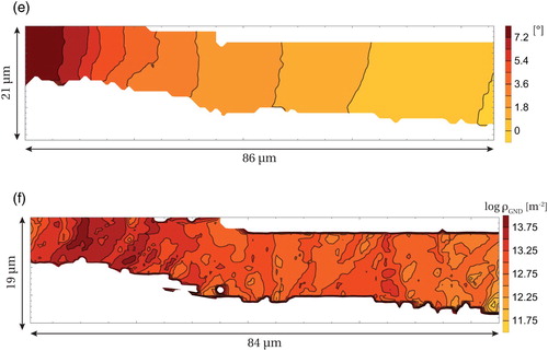
The analysis procedure was similar to that described in [Citation22, Citation23] and is based on the measurement of orientation gradients. The diffraction patterns were fitted using a MATLAB routine developed at the PSI, which provides average Euler angle values for each point of a map covering the scanned sample area. A local rotation matrix G was then calculated from these three Euler angles
:
(1)
(1)
The misorientation between two points can be described as a rotation by an angle around a rotation axis
. From the rotation matrix G, misorientation matrices
were calculated for each point across the map, using a 2D x,y coordinate system in which x,y are defined relative to a single common reference point chosen with coordinates x=0 and
, that is, situated at one end of the map and in the middle across the wire's diameter:
(2)
(2) Misorientation angles
relative to the same reference point are then computed from the trace of
:
(3)
(3) The relative rotation angles can also be expressed in the laboratory frame as rotations about x, y and z-axes, that is,
,
and
. The z-axis is assigned to the direction of the incident X-ray beam and the x-axis to the longitudinal direction of the wire.
Local misorientation vectors between the top and bottom neighbours, and right and left neighbours, of each point were also calculated:
(4)
(4) with
, ϵ the Levi-Civita permutation symbol and
the local misorientation angle. Local lattice curvatures
were then determined as
(5)
(5) with
.
From this, the local apparent density of geometrically necessary dislocations (GND) , meaning dislocations that must be present in the crystals to account for measured gradients in their local crystal orientation, is finally estimated as [Citation24]
(6)
(6) where b is the Burgers vector. GND in the context of this paper refers to unpaired dislocations that describe a local crystal orientation gradient. Note also that
is an underestimation of the actual dislocation density present locally in the samples because (i) z components are not available from the data and (ii) statistically stored (redundant) dislocations are not included.
We estimate the angular resolution to be with the undeformed (as-cast) wire and to be somewhat less fine for the deformed wires. The accuracy on
can then be estimated, with an acquisition step size
, as [Citation25]
(7)
(7) In all the results that are presented here, no recorded diffraction peaks were discarded. Most diffraction patterns exhibited more than 7 diffraction peaks, which were hence all used to calculate the orientation matrices. In the deformed wires, however, some diffraction peaks showed large variations in intensity depending on the location. This sometimes led to saturation of the detector, causing in turn the formation of a ‘ghost’ signal that was recorded at some locations situated outside of the wires, which presented only 3–4 peaks. To eliminate artefacts resulting from this effect, spectra that contained (i) only 3 peaks for the MS wire, or (ii) less than 5 peaks for SS1 and SS2 were discarded. For the SS2 wire a check was conducted to ensure that the results (ie misorientation and GND density maps) were similar when the 3 peaks ((
), (
) and (
)) that tend to be saturated were entirely excluded from the analysis; good agreement between the two sets of results was indeed found.
In the deformed microwires, we furthermore analysed the streaking of specific Laue spots, since Barabash and Ice [Citation26] showed that the streaking axis, , when resulting from the presence of unpaired edge dislocations, can be related to a specific slip system according to
(8)
(8) where
is the dislocation line vector and
the diffraction vector.
3. Results
In the as-cast microcast Al wire, misorientations were small, below . This indicates that as-cast, undeformed wires contain a low average dislocation density, of the order of
, which is close to the detection limit. Local maxima are up to one order of magnitude higher; however, these are found only in a few inclined bands a few micrometres wide. The undeformed, as-cast, wire contains overall a relatively uniform microstructure, free of visible patterns or strong variations ().
Figure 1. SEM image of a portion of the characterised as-cast microwire and contour plot of GND density over a length of 500
.
![Figure 1. SEM image of a portion of the characterised as-cast microwire and contour plot of GND density logρGND[m−2] over a length of 500 μm.](/cms/asset/81b0cc6e-c65d-4243-8e48-db8e92df07e4/tphm_a_1605220_f0001_oc.jpg)
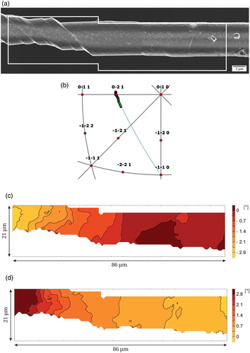
Stress-strain curves of the three deformed samples are given in the supplementary online material (SOM). Results of the post-mortem analysis of a long segment along the deformed and fractured microwire SS1, with a double slip initial orientation
that evolves into single slip, because double slip in those orientations is unstable, are shown as contour plots of misorientation angle and GND density in (b,c). The exact location where the diffraction map was acquired cannot be determined, but it lies within the visible area of the SEM image given in (a). As seen, the misorientation angle gradually increases, reaching
over a 30
distance. The longitudinal axis after deformation is found to be close to
, which is the stable orientation in tension. Post-mortem SEM images of the entire wire show the presence of a few secondary steps: some were created before the primary steps, that is, in the early stage of deformation, on a plane different than that of the primary system, while others were created after on a third, different plane. The average GND density is
m−2, peaking at values up to
locally ((c)).
Figure 2. (a) SEM image and contour plots of (b) misorientation angle [] and (c) dislocation density
in single-slip oriented microwire SS1. (d) Intensity distribution of 6 diffraction peaks at two locations (indicated by labels 1 and 2 on the above maps) and theoretical streaking directions for the glide systems a3, c5 and b2 (Schmid factors before/after deformation of respectively
0.46/0.41, 0.11/0.41 and 0.34/0); window size :
pixels.
![Figure 2. (a) SEM image and contour plots of (b) misorientation angle [∘] and (c) dislocation density logρGND[m−2] in single-slip oriented microwire SS1. (d) Intensity distribution of 6 diffraction peaks at two locations (indicated by labels 1 and 2 on the above maps) and theoretical streaking directions for the glide systems a3, c5 and b2 (Schmid factors before/after deformation of respectively ms= 0.46/0.41, 0.11/0.41 and 0.34/0); window size : 50×50 pixels.](/cms/asset/f3f4a209-3de5-4b3d-9c8a-161682211f89/tphm_a_1605220_f0002_oc.jpg)
The streaking directions of six diffraction peaks were further analysed in order to glean information about the glide systems on which dislocations are stored. Images of those 6 peaks at a given location, together with theoretical streaking directions, are given in (d); images for a full line scan throughout the analysed length are given in the SOM. One can see that the streaking directions are compatible with storage of GNDs on three possible systems, namely the two final active slip systems (designated as a3 and c5 in the figures) and/or a third slip system (b2 in the figures) that has throughout the test a lower Schmid factor and is not a cross-slip system, and is hence somewhat less expected.
The second deformed wire, also oriented for unstable double slip evolving into single-slip and of initial orientation (mechanical curve SS2 in SOM), was also scanned because, interestingly, it deformed inhomogeneously and featured a highly deformed area in the vicinity of an area almost free of visible slip steps ((a)). Hence, although this microwire had a total strain to failure lower than SS1, it is likely that in the highly deformed portion the final strain is locally roughly similar to SS1. The initial orientation is such that two glide systems have the highest Schmid factor value, namely:
and
(primary + critical systems [Citation27]). The angle between the sample axis and the glide plane of either of these two systems, that is, between
and
, is
, which is in fair agreement with the angle formed between the wire axis and the slip steps visible on the SEM image (in the range 46–56
). Two of the diffracted peaks exhibited such large variation in intensity that a rather precise location (within 1
or so) of the acquired map along the wire is possible for SS2 thanks to the large visible slip steps, and indicated with a white frame on the SEM image ((a)).
Figure 3. (a) SEM image with a rectangular frame indicating the location of the analysed area of single-slip oriented microwire SS2. (b) Stereographic projection showing the evolution of the crystal orientation along the wire's length; the markers are coloured from black to grey (green in the online version) going towards the more deformed area and the theoretical rotation of the crystal [Citation27] is indicated by the blue line joining the 0-21 and -1-10 poles (in blue in the online version). Contour plots of rotation angles [] (c)
, (d)
and (e)
. (f) Contour plot of dislocation density
.
This wire is oriented such that the beam lies almost within the principal glide plane, such that y and z directions correspond to and
directions in the crystal, respectively; it is therefore worthwhile separating components of crystal misorientation. The contour plots in (c–e) show that the rotation about the z-axis (beam axis) is higher than about the x and y axes and reaches
over the 86
length analysed. The evolution of the crystal orientation along the wire's length is plotted in the stereographic projection in (b), with the markers coloured from black to green towards the more deformed area and the theoretical rotation of the crystal indicated by the blue line [Citation27]. One can see that the longitudinal axis after deformation is close to its initial orientation in the less deformed area, while it has rotated on a great circle towards the primary
slip direction in the more heavily deformed area. The measured crystal rotation trajectory is thus in agreement with the expected path after slip on the
primary slip system; however, the spatial evolution of the crystal orientation results more likely from bending moments, whose axis coincided, for this wire, with the crystallographic plane rotation axis. Note that in the highly deformed area, the crystal orientation is such that the Schmid factor of the primary system has slightly increased (0.50 vs. 0.49 initially).
Converting local misorientation vectors to GND density values, one finds that in the highly deformed part of this wire (over the first 33 to the left of (f)) the dislocation density is on average
and goes up to
locally. The dislocation density is lower in the right-hand part, with an average of
and a maximum of
(note that the GND density map shows local variations that are not visible on the misorientation map; this is simply caused by the binning associated with the colour scales on the figures).
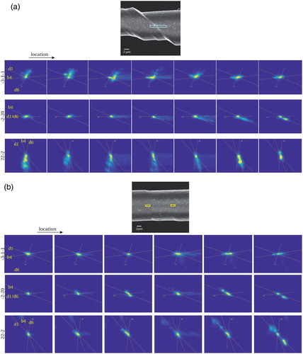
The streaking directions of 3 diffraction peaks, namely and
, are given in (a,b) for two selected areas along the SS2 wire: the first longitudinal line (within the pale blue frame) goes through the largest visible slip step and the second shows the evolution within two regions separated by a much smaller step. Additional locations and movies that show how the peaks evolve with location along a line scan going through the highly deformed portion of the wire can be found, respectively, in the SOM and at https://doi.org/10.5281/zenodo.1459734. For this wire, throughout the length that was analysed, the streaking directions are found to vary with location and result from dislocation storage on at least 3 glide systems identified as d6, d1 and b4 in the pictures; these include the primary system (d6) and a coplanar system (d1). For example, one can see in (a) that streaking evolves from d6 to b4 going from one ‘slice’ to another, and in (b) that it could be attributed to glide on d1 in the left yellow frame and evolves towards b4 in the right frame. Overall, peak streaking for sample SS2 is much reduced as compared to SS1. This probably results from the incident beam being nearly parallel to the slip planes for SS2, which reduces through-thickness variations.
Figure 4. Streaking of 3 diffraction peaks in single-slip oriented microwire SS2 (a) around the largest visible slip step and (b) within two areas separated by a small step; window size : pixels.
A third deformed wire, oriented for multiple slip ( orientation) was also analysed (mechanical curve MS in SOM). Its longitudinal axis after deformation was close to
. Although multiple glide systems are equally favoured in the
orientation, visible slip steps in the analysed area come mainly from one system, and only a few steps from other systems can be found along the whole wire (). Slip traces on Al microwires with
orientation are usually fewer and smaller compared to single slip orientations, as fewer dislocations escaped due to the high level of dislocation interactions [Citation7]. These slip traces thus indicate that 2 to 3 glide systems are activated but one predominates, which differs from bulk
single crystals where an almost equal operation of the 3 possible glide directions was reported, enabling deformation to proceed without any crystal rotation [Citation28, Citation29]. Here, misorientation angles reach values up to
and are far more irregularly distributed than in wires oriented for single slip. The average geometrically necessary dislocation density is higher, namely
, reaching up to
locally. Analysis of the streaking directions of the diffracted spots shows that there is no clear streaking direction for most of the peaks (in areas of both lower and higher
). Hence, and not surprisingly, dislocations storage in this wire results from activity along multiple slip systems; it is also higher and the misorientation map shows that the substructure is more irregular within this wire.
Figure 5. SEM image of a deformed microwire initially oriented for multiple-slip; contour plot of misorientation angle [] (left) and dislocation density
(right).
![Figure 5. SEM image of a deformed microwire initially oriented for multiple-slip; contour plot of misorientation angle [∘] (left) and dislocation density logρGND[m−2] (right).](/cms/asset/a448122b-cb35-44f6-ac2b-dc2f3f843d10/tphm_a_1605220_f0005_oc.jpg)
4. Discussion
In the as-cast (undeformed) wire, dislocation densities measured here () are higher than what was found in [Citation7] on two TEM lamellae extracted by means of focused ion beam milling from as-cast wires 14
in diameter: values from the TEM lamella were
(
). The value derived from the present measurements is in principle a lower bound estimator of the initial GND density in the as-cast wires; however, it is important to note that this value is close to the theoretical detection limit of the present Laue microdiffraction data (see Equation (Equation7
(7)
(7) )), such that the actual average GND value in the undeformed wires might be lower than
.
Dislocation densities measured in [Citation7] in TEM samples of deformed wire were in the range 1.7–1.8 for a deformed wire 15
in diameter oriented along the
direction. These values are somewhat on the low side, but consistent with the (far more extensive) data given here.
Overall, GND densities that we measure by Laue microdiffraction in the deformed microwires are quite high, given that microcast wires contain no ion-milling surface artefacts and have a sufficiently high aspect ratio to deform nominally under essentially uniform stress and strain, with large amounts of slip occurring along discrete planes but no slip gradients along those planes nor visible orientation gradients within the deformed crystals. High GND densities might be explained by the high strain to failure of the present microwires and by the fact that the thin layer of native oxide along their surface might have prevented dislocation escape. If no dislocation would escape the microwires, a lower bound of the mobile dislocation density needed to produce a given strain to failure can be estimated as ρ=2
, if we give each dislocation within the wire a length of
. With
roughly 0.8 and 0.6 for single slip and multiple slip oriented wires, respectively, the measured GND densities correspond to 2.5 and 10% of the value thus estimated for the required mobile dislocation density ρ. Although GND values are lower bounds on the actual stored dislocation density within the wire, the difference between the two values is sufficiently high for the conclusion to be reached that most dislocations escaped the microcast wires while they were being deformed in tension. A similar conclusion was found by Kirchlechner et al. [Citation19] by analysing peak streaking during tensile deformation of Cu single microcrystals (aspect ratio of 1:5) initially oriented for single slip.
In this work we also observe significant differences between wires nominally oriented for single slip, one having deformed to roughly the same strain along its entire length (SS1), while the other has produced more inhomogeneous deformation (SS2). Wire SS1 has traversed (more uniformly but going farther) the stereographic triangle and is finally oriented near , that is, along the
border of the stereographic triangle. Hence there is, after deformation, stable double slip active on this system in this wire, and it is therefore not surprising that there be significant dislocation storage on what was initially the primary glide system (the 2 active slip systems form Lomer locks).
The measured GND densities and distributions are overall consistent with the interpretation of the deformation behaviour of microcast wire crystals that was offered in [Citation7], namely that dislocation mechanisms underlying the deformation of those wires are to a significant extent driven by the activation of single-arm sources inhomogeneously distributed along the wire length. Storage of GNDs is indeed found to occur (albeit not exclusively) in the primary slip system in deformed single slip oriented microwires, as evidenced by the peak streaking directions. This is consistent with the dislocation dynamics (DD) simulations presented in [Citation7] where dislocation debris, leading to the formation of the so-called braid structure, were found to be left in the active slip systems. Also consistent with the interpretation given in [Citation7] is the observation that the GND density is higher in the wire oriented for multiple slip. In multislip samples, which exhibit fewer large slip steps and smaller strain bursts, single-arm sources operate fewer revolutions before being shut down, necessitating the activation of a greater number of sources for a given accumulation of strain, leading hence to greater rates of dislocation accumulation, both features coming from the fact that cross-slip and lock formation are more frequent in the than in single-slip orientations [Citation7, Citation10, Citation30, Citation31].
5. Conclusion
As-cast and deformed microwires of pure aluminium are characterised by means of Laue synchrotron X-ray microdiffraction maps gleaned over selected areas of the wires. Data show that:
in the as-cast condition, the wires contain a low density of geometrically necessary dislocations, situated slightly below
;
after deformation, the geometrically necessary dislocation density in the microcast wires has increased, reaching around
measured GND density values are well below what would be stored were dislocations prevented from escaping along the surface during the deformation of the single-slip wires. It is higher in the multislip sample oriented along
Those observations are consistent with the deformation mechanism that was proposed in [Citation7], namely that deformation in these crystals is largely driven by repeatedly rotating, likely single-arm, sources which enable most moving dislocations to escape through the free surface, particularly if the wire is oriented for single slip.
Acknowledgments
The authors thank Dr Kurt Schenk for single-crystal X-ray diffraction measurements.
Disclosure statement
No potential conflict of interest was reported by the authors.
Additional information
Funding
References
- L.P. Kubin, Dislocations, Mesoscale Simulations and Plastic Flow, Oxford University Press, Oxford, 2013.
- M.D. Uchic, P.A. Shade, and D.M. Dimiduk, Plasticity of micrometer-scale single crystals in compression, Ann. Rev. Mater. Res. 39 (2009), pp. 361–386. Available at https://doi.org/10.1146/annurev-matsci-082908-145422.
- G. Dehm, Miniaturized single-crystalline fcc metals deformed in tension: New insights in size-dependent plasticity, Prog. Mater. Sci. 54 (2009), pp. 664–688. Available at http://www.sciencedirect.com/science/article/pii/S0079642509000176. doi: 10.1016/j.pmatsci.2009.03.005
- O. Kraft, P.A. Gruber, R. Mönig, and D. Weygand, Plasticity in confined dimensions, Ann. Rev. Mater. Res. 40 (2010), pp. 293–317. Available at https://doi.org/10.1146/annurev-matsci-082908-145409.
- J.R. Greer and J.T.D. Hosson, Plasticity in small-sized metallic systems: Intrinsic versus extrinsic size effect, Prog. Mater. Sci. 56 (2011), pp. 654–724. doi: 10.1016/j.pmatsci.2011.01.005
- C.R. Weinberger and W. Cai, Plasticity of metal nanowires, J. Mater. Chem. 22 (2012), pp. 3277–3292. Available at http://dx.doi.org/10.1039/C2JM13682A.
- J. Krebs, S. Rao, S. Verheyden, C. Miko, R. Goodall, W. Curtin, and A. Mortensen, Cast aluminium single crystals cross the threshold from bulk to size-dependent stochastic plasticity, Nat. Mater. 16 (2017), pp. 730–736. doi: 10.1038/nmat4911
- T.A. Parthasarathy, S.I. Rao, D.M. Dimiduk, M.D. Uchic, and D.R. Trinkle, Contribution to size effect of yield strength from the stochastics of dislocation source lengths in finite samples, Scripta Mater. 56 (2007), pp. 313–316. Available at http://www.sciencedirect.com/science/article/pii/S1359646206006853. doi: 10.1016/j.scriptamat.2006.09.016
- H. Tang, K.W. Schwarz, and H.D. Espinosa, Dislocation-source shutdown and the plastic behavior of single-crystal micropillars, Phys. Rev. Lett. 100 (2008), p. 185503. Available at https://link.aps.org/doi/10.1103/PhysRevLett.100.185503.
- C. Motz, D. Weygand, J. Senger, and P. Gumbsch, Initial dislocation structures in 3-d discrete dislocation dynamics and their influence on microscale plasticity, Acta Mater. 57 (2009), pp. 1744–1754. Available at http://www.sciencedirect.com/science/article/pii/S1359645408008872. doi: 10.1016/j.actamat.2008.12.020
- S. Oh, M. Legros, D. Kiener, and G. Dehm, In situ observation of dislocation nucleation and escape in a submicrometre aluminium single crystal, Nat. Mater. 8 (2009), pp. 95–100. doi: 10.1038/nmat2370
- D. Kiener and A. Minor, Source-controlled yield and hardening of Cu(1 0 0) studied by in situ transmission electron microscopy, Acta Mater. 59 (2011), pp. 1328–1337. doi: 10.1016/j.actamat.2010.10.065
- F. Mompiou, M. Legros, A. Sedlmayr, D. Gianola, D. Caillard, and O. Kraft, Source-based strengthening of sub-micrometer al fibers, Acta Mater. 60 (2012), pp. 977–983. doi: 10.1016/j.actamat.2011.11.005
- S. Rao, D. Dimiduk, T. Parthasarathy, M. Uchic, M. Tang, and C. Woodward, Athermal mechanisms of size-dependent crystal flow gleaned from three-dimensional discrete dislocation simulations, Acta Mater. 56 (2008), pp. 3245–3259. Available at http://www.sciencedirect.com/science/article/pii/S1359645408002024. doi: 10.1016/j.actamat.2008.03.011
- J. El-Awady, Unravelling the physics of size-dependent dislocation-mediated plasticity, Nat. Commun. 6 (2015). Article number 5926. doi: 10.1038/ncomms6926
- R.I. Barabash, G.E. Ice, and F.J. Walker, Quantitative microdiffraction from deformed crystals with unpaired dislocations and dislocation walls, J. Appl. Phys. 93 (2003), pp. 1457–1464. Available at http://dx.doi.org/10.1063/1.1534378.
- H. Van Swygenhoven and S. Van Petegem, The use of Laue microdiffraction to study small-scale plasticity, J. Met. 62 (2010), pp. 36–43.
- R. Maaß, S. Van Petegem, H. Van Swygenhoven, P.M. Derlet, C.A. Volkert, and D. Grolimund, Time-resolved laue diffraction of deforming micropillars, Phys. Rev. Lett. 99 (2007), p. 145505. Available at https://link.aps.org/doi/10.1103/PhysRevLett.99.145505.
- C. Kirchlechner, D. Kiener, C. Motz, S. Labat, N. Vaxelaire, O. Perroud, J.S. Micha, O. Ulrich, O. Thomas, G. Dehm, and J. Keckes, Dislocation storage in single slip-oriented cu micro-tensile samples: new insights via x-ray microdiffraction, Phil. Mag. 91 (2011), pp. 1256–1264. doi: 10.1080/14786431003785639
- C. Kirchlechner, P. Imrich, W. Grosinger, M. Kapp, J. Keckes, J. Micha, O. Ulrich, O. Thomas, S. Labat, C. Motz, and G. Dehm, Expected and unexpected plastic behavior at the micron scale: An in situ μ Laue tensile study, Acta Mater. 60 (2012), pp. 1252–1258. doi: 10.1016/j.actamat.2011.10.058
- J. Wheeler, C. Kirchlechner, J.S. Micha, J. Michler, and D. Kiener, The effect of size on the strength of fcc metals at elevated temperatures: Annealed copper, Phil. Mag. 96 (2016), pp. 3379–3395. doi: 10.1080/14786435.2016.1224945
- W. Pantleon, Resolving the geometrically necessary dislocation content by conventional electron backscattering diffraction, Scr. Mater. 58 (2008), pp. 994–997. doi: 10.1016/j.scriptamat.2008.01.050
- A. Irastorza-Landa, H. Van Swygenhoven, S. Van Petegem, N. Grilli, A. Bollhalder, S. Brandstetter, and D. Grolimund, Following dislocation patterning during fatigue, Acta Mater. 112 (2016), pp. 184–193. doi: 10.1016/j.actamat.2016.04.011
- V. Gupta and S. Agnew, A simple algorithm to eliminate ambiguities in ebsd orientation map visualization and analyses: Application to fatigue crack-tips/wakes in aluminum alloys, Microsc. Microanal. 16 (2010), pp. 831–841. doi: 10.1017/S1431927610093992
- A.J. Wilkinson and D. Randman, Determination of elastic strain fields and geometrically necessary dislocation distributions near nanoindents using electron back scatter diffraction, Phil. Mag. 90 (2010), pp. 1159–1177. Available at http://dx.doi.org/10.1080/14786430903304145.
- R. Barabash and G. Ice, Strain and Dislocation Gradients from Diffraction: Spatially-Resolved Local Structure and Defects, Imperial College Press, London, 2014.
- W.F. Hosford, The Mechanics of Crystals and Textured Polycrystals, Oxford University Press, New York - Oxford, 1993.
- W. Hosford, R. Fleischer, and W. Backofen, Tensile deformation of aluminium single crystals at low temperatures, Acta Metall. 8 (1960), pp. 187–199. doi: 10.1016/0001-6160(60)90127-9
- U. Kocks, Polyslip in single crystals, Acta Metall. 8 (1960), pp. 345–352. doi: 10.1016/0001-6160(60)90001-8
- R. Madec, B. Devincre, L. Kubin, T. Hoc, and D. Rodney, The role of collinear interaction in dislocation-induced hardening, Science 301 (2003), pp. 1879–1882. Available at http://science.sciencemag.org/content/301/5641/1879. doi: 10.1126/science.1085477
- B. Devincre, T. Hoc, and L.P. Kubin, Collinear interactions of dislocations and slip systems, Mater. Sci. Eng. A 400 (2005), pp. 182–185. Available at http://www.sciencedirect.com/science/article/pii/S0921509305003333. doi: 10.1016/j.msea.2005.02.071