
 ?Mathematical formulae have been encoded as MathML and are displayed in this HTML version using MathJax in order to improve their display. Uncheck the box to turn MathJax off. This feature requires Javascript. Click on a formula to zoom.
Abstract
The electronic properties of eight chosen naphthalene derivatives carrying one or two hydroxyl groups have been determined experimentally and theoretically using experimental data and computer simulations. The measurements of the transient photocurrents and steady state dark currents were made. The results of quantum density functional theory calculations based on the Marcus–Hush theory were used to calculate Einstein's mobility. The analysis of the Hirshfeld surface allowed to determine the probable influence of the nature of the substituents and the substituent position on the conductivity of the tested naphthalenes. The results allowed for a qualitative determination of the nature of the hole transport mechanism.
1. Introduction
Aromatic compounds are well described in the area of their basic chemical properties. The ability to modulate their properties as a result of a change in the geometry of molecule and of the change in the type of substituent ensures the possibility of obtaining the desired material properties according to their applications [Citation1–3]. Low molecular materials are made of molecules with unchanging structure and with strictly defined dimensions. In the aforementioned types of compounds, a group of polycyclic aromatic hydrocarbons (PAH) characterized with significant molecular weight and well-known chemical and physical properties is distinguished [Citation2, Citation4–6] and among them linear acenes that are in strong interest in electronic technology [Citation6–11]. Molecules of PAH meet the condition, having a π-electron conjugated bonding system necessary for appearance their semiconductor properties [Citation4, Citation8, Citation12].
Transport of charge carriers in layers of molecular material depends on the structure of molecules and packing of crystals as well as intermolecular interactions between them [Citation1, Citation2, Citation7–10]. The theoretical analysis applying modeling of the electronic properties of the organic materials needs empirical verification of the mechanism for the charge transfer transport.
Condensed state, and in particular a crystal is formed from free molecules, charge redistribution occurs in order to create the conditions for the appearance of van der Waals forces, which is also revealed in the charge state of the atoms that molecule consists of. On the basis of the above, it was established that the mechanism of chemical bond formation in molecular crystals consists of two intramolecular and intermolecular components. To define the mechanism of chemical bond formation, it is convenient to use quantum chemical software products [Citation13], e.g. Gaussian09 [Citation14] capable of performing density functional theory (DFT) calculations.
The problem of measuring the mobility and concentration of carriers in naphthalene and its derivatives is most often considered in relation to crystalline samples in the range of low temperatures. The measurements of charge carrier mobility of monocrystalline naphthalene samples were carried out using the Hall effect method and the method of instantaneous currents generated by an photon impulse [Citation15]. The obtained drift mobility values for holes in the naphthalene were in the order of 10−1 cm2/Vs at room temperatures. The same order of mobility values was obtained from theoretical analysis ab initio of the charge transport for monocrystals af acenes [Citation16, Citation17]. It must be noticed that there is lack of the measurements at room temperatures of the electrical properties of thin layers composed of naphthalene substituted with noncomplex chemical groups.
Naphthalene derivatives with at least one -OH substituent chosen for this study were divided into two classes. The class 1 (dihydroxynaphthalenes) carrying two –OH substituents and the class 2 with only one -OH substituent (see and ). The comparison of the properties of the tested meta- and para-substituted derivatives with the peri-substituted derivative () was made in this work.
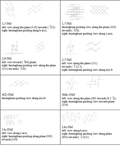
Figure 1. Structural scheme of compounds.
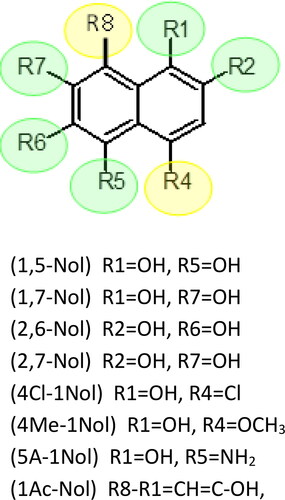
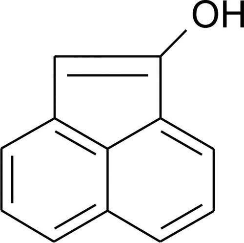
Figure 2. 1-hydroxyacenaphthen (1Ac-Nol).
An attempt was made to explain the influence of the structure of the molecule under investigation on noncovalent intermolecular interactions in the layers with use of the X-ray powder diffraction analysis (XPRD analysis) and Hirshfeld surface analysis [Citation18].
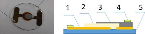
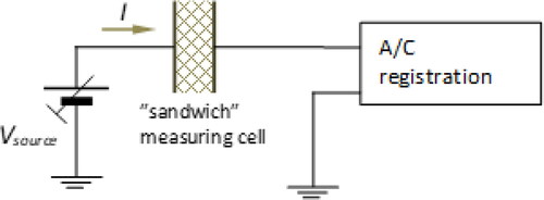
The time of flight (TOF) method [Citation4, Citation19] combined with the dark current-voltage (I-U) measurements in the space charge limited current (SCLC) regime [Citation19–22] were used for measurements of electric properties. The samples used for measurements were built as a layered “sandwich” structures (). The biasing voltage given to the external metallic electrodes was polarized the measured layer.
Figure 3. Photo (a) and section of the measuring cell (b) (1- Au electrode, 2-studied layer, 3- Al electrode, 4- In contact, 5-glass substrate).
Theoretical calculations were made on the basis of DFT quantum-chemical calculations for the isolated molecules using Gaussian09 [Citation14] at the B3LYP/6-311++G(d,p) level of theory.
The properties of the frontier molecular orbitals (FMO) and the values of reorganization energies (Er) were determined as in the works by Datta et al. [Citation9] and Deng and Goddard [Citation11], where the Marcus [Citation23] and Hush [Citation24] theories were applied to determine the nature of the charge transfer process [Citation11, Citation25, Citation26]. The results of the aforementioned calculations allowed for the analysis of the nature of the electric charge transfer process in a manner similar to that presented by Deng and Goddard [Citation11], Ren et al. [Citation25] and Mendels and Tessler [Citation26] and Campbell et al. [Citation3] and Rossi and Sohlberg [Citation27].
The crystal structure of all studied compounds is known [Citation28–34]. The reports concerning the crystal and molecular structure of dihydroxynaphthalenes which we call the class 1 of the described compounds, i.e. 1,5-dihydroxynaphthalene (1,5-Nol), 2,6-dihydroxynaphthalene (2,6-Nol) are shown by Belskii et al. [Citation29], 1,7-dihydroxynaphthalene (1,7-Nol) is shown in [Citation28] and 2,7-dihydroxynapthalene (2,7-Nol) is shown at [Citation30]. The class 2 of naphthalene derivatives with two different substituents, of which only one containing the -OH group, form the following compounds: 4-methoxy-1-naphthol (4Me-1Nol) with crystal structure described in [Citation31], 4-chloro-1- hydroxynaphthalene (4Cl-1Nol) in [Citation32] and 5-amino-1- hydroxynaphthalene (5A-1Nol) in [Citation33]. The crystal structure of 1-hydroxyacenaphthen (1Ac-Nol) with bridged peri-substituent groups was described in [Citation34].
Hirshfeld surface analysis [Citation18, Citation35, Citation36] was undertaken on the basis of a detailed crystalline structure of material and allowed to determine the arrangement of the molecules in the layer [Citation25] and also to determine the influence of noncovalent intermolecular interactions on the electrical properties of the material. The XPRD analysis enabled to determine the structure of the obtained layers, including the arrangement of molecules in relation to the substrate and to quantify the size of the grains in the layer [Citation12, Citation37–39]. The effective values of the mobility of the charge carriers should show a dependence on these quantities [Citation40]
The electrical properties of the presented compounds in the form of the thin polycrystalline layers were carried out in air at room temperatures and at the humidity of 45–55%. Therefore, it is difficult to compare the obtained values of mobility and conductivity for similar compounds with the results obtained in earlier works describing the measurements carried out on nanocrystals in lower temperatures. The measurements were carried out at typical working conditions for the electronic devices.
2. Experiment and calculations
2.1. Materials and sample preparations
2.1.1. Materials
Naphthalene derivatives (considered in conjunction with 1-acenaphthenol) chosen for measurements are distinguished by the rigid skeleton creating the conjugated system of the π bonds and composed of linearly ordered two benzene rings, and . The naphthalene conjugated system in derivatives selected is extended by replacement of the ring hydrogens by unsaturated group (-OH, -Cl, -NH2, -OCH3). in which unsaturated electron pairs are to some extend delocalized to become a part of the aromatic π - electron system in both the ground and excited states. The effects of the two substituents should be additive on the electric transport properties.
It was not possible to obtain experimentally layers of peri-substituted naphthalene without bridging with the quality required for electrical measurements. Therefore, 1AcNol was selected as the peri-substituted naphthalene. We consider 1AcNol as 10-π-electron naphthalene core connected to 2-π-electron etheno system carrying one -OH group [Citation5] in this work.
The derivatives selected for studies were commercially available as materials with a purity of 97–99% and were purchased from Aldrich (1,5-Nol; 1,7-Nol; 2,6-Nol, 2,7-Nol, 4Cl-1Nol, 1Ac-Nol) and Fluka (2,7-Nol, 4Me-1Nol, 5A-1Nol) and have been additionally purified. Material was recrystallized from distilled benzene and anhydrous ethanol, and then, it was passed through chromatographic column filled with Al2O3, and then, dried in vacuum. Gas chromatography (Hewlett Packard 58900 series II gas chromatograph equipped with mass spectrometry detector) reveals the total impurity contents below 10−3 wt. %.
2.1.2. Preparation of samples
Layers of the eight naphthalene derivatives has been obtained with thermal vacuum deposition method with the temperature of the vaporization of the organic material below 600 K. Low temperature of vaporization process allows for limitation of the effect of the unwanted external influences. The plates of quartz glass with thickness of 1 mm with previously vaporized Au layer used as one of the electrodes were used as the substrates.
The second one, the optically semi-transparent electrode made of Al, was vaporized directly on the examined layer. Both measurement electrodes and examined layer were deposited in the vacuum of 10−5 Tr. Thermal vacuum deposition method enables to obtain good electric contact of the measured layer with the measuring electrodes. Evaporation of the Au or Al electrodes was accomplished from tungsten wire, where the vaporized material with the purity of 4 N for Au and 5 N for Al was wounded over. Thermal evaporation of organic layer was done from quartz crucible. The substrate temperature was in the proximity of 300 K, and the rate of evaporation was about 10 nm/s. This choice of substrate temperature corresponded to the temperature at which electrical measurements were carried out.
2.2. XPRD measurements
The quality of the layers was determined using XPRD. Diffraction patterns of thin layers of examined hydrocarbons were collected in Bragg–Brentano geometry by powder diffractometer HZG-4 with computer data processing DRONEK. X-ray data were collected in the range of the scanning angle 2θ = 5° − 50° with the scanning step of 0.02°. XPRD technic enabled to asserts information on the measured sample:
quality of organic layer (crystalline or amorphous)
grain size in the crystalline layer
the purity of the layer
2.3. Electrical measurements
Measurements of the electrical properties of organic materials have been made using measuring cells, , where the layered structure formed a “sandwich” in the form of metal layer-organic layer-metal layer. The measuring cell, was formed a plate capacitor with plates of surface near 0.5 cm2. The layer of organic material (3) was deposited on the glass substrate (5) previously supplied with Au electrode (1). Then, on such an organic layer was deposited semitransparent Al layer, and then, the In contacts (4) were soldered.
The electrical capacity for such cells, was measured with use of Semi-Automatic RLC Bridge type E314. The thickness of the organic layer was estimated based on the relationship
(2.1)
(2.1)
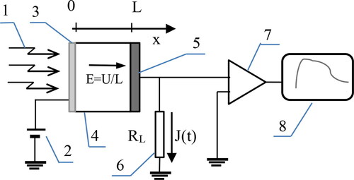
where L – thickness of the organic layer, ε – relative dielectric constant, ε0 – vacuum dielectric constant, S – surface of the electrode, C – measured capacity. The thicknesses of the studied layers were in the range within about 1 µm to 40 µm. According to [Citation41, Citation42] the relative dielectric constant was taken for calculations as ε = 3. The TOF measurements [Citation1, Citation43, Citation44] were exploited for determination of the hole mobility. UV light pulse was induced the current intensity through the thin layer of the material. Information scheme of the measuring setup is shown in the . UV light flash (1) shorter than the duration of the registered transient through the layer generates an excess charge. The transporting electric field E generated inside the measured layer by the biasing the measuring cell by a UB voltage supplied by a low noise supplier (2) forces the separation of the charge carriers near the illuminated semitransparent electrode (3) and causes drift of thin “sheet” of the moving charge carriers through the layer of the studied organic material. The total current passing through the electrode (5) forces the drop of potential through the resistor RL (6) whose resistance value is known (RL=1MΩ). The potential drop registered by a digital oscilloscope (7) is scaled directly in the units of the current intensity and is saved in the computer (8) that controls signal acquisition.
Figure 4. Measuring set-up applied for studying of the transient photocurrents (J(t): 1- UV light flash, 2- direct current supplier, 3- semitransparent Al electrode, 4- the layer of studied organic material, 5- Au electrode, 6- load resistor, 7- oscilloscope, 8- computer that controls signal acquisition.
The second method of measurements, i.e. dark current voltage (U-I) characteristics () is complementary to the above discussed TOF method. It allows a wide interpretation of electrical properties in the range of space charge limited currents (SCLC) [Citation2, Citation19–22, Citation45]. Microscopic parameters such as the free carrier’s concentration, trap filling coefficient, resistivity of material and density of states (DOS) and the type of charge transport were determined on that basis. The method of analyzing the experimental data using differentiation of obtained current-voltage characteristics presented in the doubly logarithmic scale allows for determination of the aforementioned parameters.
Figure 5. Measuring setup scheme for determination of dark current-voltage (I-U) characteristics.
2.3.1. TOF measurements
The application of the TOF method for measuring current-time characteristics I-t with eliminating the effect of the time constant of the measuring system [Citation44], enables determination of the time of flight (τTOF) as a function of polarization voltage (U) or the life-time of charge carriers (τf). The advantage of this method is that it enables the analysis of the current transients irrespective of the direct influence of electrodes, therefore, the obtained data correspond only to the properties of the material under examination. Generation of carriers occurs only near the illuminated electrode when the UV radiation is strongly absorbed in the studied material. A completely different interpretation of the obtained data is used when the charge carriers of both signs are not generated near the illuminated electrode, but in volume of the studied sample. The characteristic time determined in that case will be independent on the polarization voltage. The characteristic time obtained in this way cannot be interpreted as the time of flight and use directly to determine mobility value. According to the Fritzsches’ theory [Citation43], the characteristic time obtained from such measurement is the lifetime of carriers, which can be used directly to calculate Einstein's mobility (i.e. the mobility dependent on diffusion coefficient). The TOF measurements for the compounds shown in the for the class 1 of our tested compounds allowed direct determination of the time of flight for layers with a proper magnitude of thick. This measurements were possible for thinner layers due to application splines with considering the impact of the RC time constant [Citation44]. This approach allowed to determine the drift mobility of holes in tested materials.
Table 1. Crystal structure of the compounds and the XPRD data obtained for measured naphthalene derivatives with two OH substituents (class 1).
The lifetimes for two naphthalene derivatives from the class 2 of compounds, shown in , i.e. 4Cl-1Nol and 5A-1Nol and of 1,7-Nol and 2,7-Nol thinner than 1 µm were measured. The knowledge of this quantities enabled to determine the Einstein mobility. However, the accuracy of determination of this mobility is much lower than for the drift mobility. For the thicker layers of 1.7-Nol and 2.7-Nol (with thicknesses above 25 µm) determination of the time of flight enabled direct assessment of the drift mobility.
Table 2. Crystal structure of the compounds and the XPRD data obtained for measured naphthalene derivatives with two different substituents (class 2).
2.3.2. Trap spectroscopy calculations (DM-SCLC)
The characteristics (I-U) obtained as a result of measurements of the dark equilibrium currents in the SCLC range were used to obtain results from trap spectroscopy using a calculation procedure with differential method of space charge limited currents (DM SCLC) [Citation19–21].
The decisive for correctness of the DM-SCLC calculations is possibility for determining smooth derivatives of coefficients, i.e. α, α′ α″ calculated after the transformed characteristics of the J-U (where J is obtained after recalculation of the I experimental values to the J = I/A, where J-density of the current, A- surface of the electrodes) to the double logarithmic scale, lnJ- lnU:
(2.2)
(2.2)
The cubic spline interpolation method allows to obtain smooth derivatives α, α′, α″. Cubic splines minimizes bending of the line passing through multiple two-dimensional experimentally determined nodes (U, J), and ensures the continuity of the first and second derivatives at each point of sticking polynomials.
The DM-SCLC analysis of such transformed experimental data used the set of the equations [19–21]:
(2.3)
(2.3)
(2.4)
(2.4)
(2.5)
(2.5)
where e is the electron charge, µd is the drift mobility of charge carriers (in this paper taken from our TOF measurements), L is the sample thickness, ε0 is dielectric constant, ε is the dielectric permittivity of the material, nf is the concentration of free charge carriers at the cathode, ns is the actual concentration of carriers trapped by local states near cathode, ρL is the space charge density limiting the current.
The values of free carrier concentration nf, trap concentration ns and trap filling coefficient θ, have been calculated from experimental data. Knowledge of them allows to determine mobility and conductivity values.
The analysis of the U-I characteristics, when assuming the existence of one trap level, shows a strong increase for the voltage Vi at when the traps are filled.
The maximum possible concentration of charge carriers n0 injected by the electrode until the current is limited by the space charge is determined as:
(2.6)
(2.6)
The specific conductivity σ, defined in the SCLC range as
(2.7)
(2.7)
where E = U/L, is important for the analysis of the electrical matching of layers in electronic systems.
The analysis of the results of dark current measurements using the DM-SCLC method required interpolation with the use of cubic splines.
Selected summary of the results of constant dark current measurements using the splines in DM-SCLC related to the tested compounds for the layers from both class 1 and class 2 are presented in and .
Table 3. Electric properties of naphthalene derivatives belonging to the class 1.
Table 4. Electric properties of naphthalene derivatives belonging to the class 2.
2.4. DFT calculations
DFT calculations for gas state molecules enables to obtain the shapes of HOMO and LUMO orbitals and the spatial distribution of the electron levels necessary for the application of the Marcus–Hush theory [Citation9, Citation23–25], to determine the parameters of charge carrier transport. The quantities defining the hole transport, i.e. reorganization energy Er for a hole transport, the value of the transfer integral Jij and the charge transfer rate Kij+ allowed for theoretical determination of the holes mobility for the studied naphthalene derivatives.
The charge transfer rate for hopping transport can be calculated as:
(2.8)
(2.8)
where
Ke - the charge transfer rate of the hopping of the charge carriers (holes or electrons) between neighboring molecules,
Jij - the transfer integral between neighboring i and j molecules,
Er - the reorganization energy of the molecule during transfer of the hole/electron,
T – temperature in Kelvin,h – Planck constant (6.62⋅× 10−34 Js),kB –Boltzmann constant (1.38⋅× 10−23 JK−1).
The results of the calculations are illustrated in and . The calculated values of reorganization energy do not differ significantly from the results obtained earlier for acenes having a similar aromatic skeleton structure [Citation7, Citation11, Citation25, Citation27].
Table 5. Reorganization energy, transfer integral values and charge transfer rate for the naphthalene derivatives for the class 1 obtained with DFT calculations on the B3LYP/6-311++G(d,p) level of theory.
Table 6. Reorganization energy, transfer integral values and charge transfer rate for the naphthalene derivatives for the class 2 obtained with DFT calculations on the B3LYP/6-311++G(d,p) level of theory.
Table 7. Einstein and drift mobility for charge carriers and trap filling coefficient registered for the layers of studied materials from the class 1.
The strong dependence of mobility of carriers on aforementioned parameters Er, Ke, Jij exists in accordance with [Citation3, Citation11, Citation46]. Mobility depends much stronger on the first two parameters (reorganization energy and charge transfer rate) and much less on the transfer integral in the case of hopping transport. The DFT calculations showed that of the tested class 2 compounds, the 1Ac-Nol had the lowest reorganization energy Er and at the same time the highest hopping rate Ke (). The measurements revealed that it has the highest value of drift mobility, see the .
Table 8. Einstein and drift mobility for charge carriers and trap filling coefficient registered for the layers of studied materials from the class 2.
This suggests that indeed higher mobility values are possible during transport of holes when reorganization energy Er is low, the hopping rate Ke is high and the transfer integral value (Jij) is large enough.
2.5. Hirshfeld surface analysis
Hirschfeld's surface analysis [Citation18, Citation35, Citation36] was also performed for the studied naphthalene derivatives. The statistical evaluation of the rate of intermolecular contacts seen in the Hirshfeld surface of naphthalene derivatives presented in and allows to perform a quantitative analysis of the relationship between the substitution parameters and the nature of interactions between adjacent molecules.
Figure 6. Statistics of relative contribution to the Hirshfeld Surface area for the various close intermolecular contacts in naphthalene derivatives from the class 1.
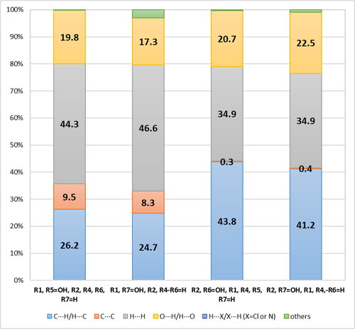
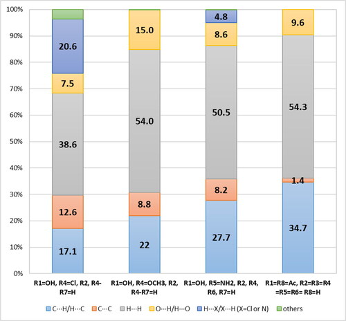
Figure 7. Statistics of relative contribution to the Hirshfeld Surface area for the various close intermolecular contacts in naphthalene derivatives from the class 2.
The analysis of the Hirshfeld surface concerns the interactions in the immediate vicinity of the molecules. Therefore, it can be used with some approximation to determine the properties of the polycrystalline and amorphous material. In such materials, the grain size is specified. The interactions in the immediate vicinity of the molecule inside each grain are similar to those of the molecule in a monocrystalline material. However, there is a distortion disturbing the periodicity resulting from the spatial limitation of the crystal grain [Citation38, Citation39].
The Hirshfeld analysis indicates that the modification of the molecule of dihydroxy - naphthalene derivatives having both -OH groups in the position α, which consists in changing the position of at least one of these substituents in the β position, causes on average a 24-fold increase in the participation of C·· C contacts and the accompanying average of about a 42-fold reduction in the ratio (% C · H)/(% C · C). Such a change is associated with the appearance of pi-stacking arrangement of molecules, which is favorable due to the possibility of obtaining higher mobility of charge carriers.
The analysis of the relative contribution to the Hirshfeld surface of the close intermolecular contacts in the crystal of 4Cl-1Nol facilitates substantial contribution of the H-Cl/Cl-H contacts of 20.6% of Hirshfeld surface, but contribution of the H-H contacts is low of 38.6%. It is observed the strong and nearly linear contact O-H⋯H-O, connecting the H atom of the hydroxyl group of the one molecule with the O atom of the hydroxyl group of the neighboring molecule. We suppose that the contribution of the different kind of contacts should affect the decrease of the surface diffusion constant of the molecules during the crystallization. This should promote the generation of many isolated crystallization centers [Citation47] and in the consequence formation of the amorphous structure of the layers of 4Cl-1Nol. The Hirshfeld surface analysis connected with the results of crystal analysis [Citation34] and extended Marcus–Hush theory presented in [Citation18] allows an attempt to explain relatively high drift mobility of the layers of 1Ac-Nol.
The 1Ac-Nol layers of compounds showed no pi-stacking overlap. Nevertheless, this compound shows the greatest drift mobility among the class 2.
The 1Ac-Nol molecule is flat, but the oxygen atom O1 of the hydroxyl group deflects out of the plane defined by the naphthalene skeleton of the molecule by a 1.105 Å [Citation29]. Crystallographic description [Citation34] indicates that in the crystal of 1Ac-Nol there is hydrogen bond O1-H1···O1 (where the distances are d O···H = 0.82 Å, d H···O = 1.97 Å and d O-H···O = 2.771 Å and angle O-H···O, is 170°) and two C-H···π bonds. Analysis of the molecular Hirshfeld surface confirms the existence of H···C/C···H (34.7%) close intermolecular contacts. Such a significant participation of C···H contacts relates to the presence of the C-H···π interaction. X ray analysis [Citation41] indicated that the interactions O-H···O/O···O-H, stabilized mainly by C H···π, are the origin of generation of the infinite spiral chain structure of contacts between molecules forming in [010] direction ordered chain of the molecules connected to each other with a spiral pitch of one lattice constant [Citation34].
The analysis of the Hirshfeld surface concerns the interactions in proximity of the molecules. Thus, it is useful for determining the properties of polycrystalline and amorphous materials. The interactions in the proximity of the molecules in such materials are similar to that in the proximity of the molecule of monocrystalline material, but a distortion that disturbs the periodicity should be observed [Citation38, Citation39].
3. Results and discussion
The XPRD powder method allowed for the estimation of the size of the grains present in the tested layers. The powder diffractograms obtained with this method are presented in . The properties of the crystalline structure of the tested compounds are presented in and and crystal packing in the (the plane parallel to the substrate surface is shown for crystalline layers). The quantitative analysis of such diffraction patterns requires the knowledge of the crystal structure of the single crystals of the tested compounds. The quantitative evaluation of the mean size of the grains forming the tested layers was determined using the Scherrer equation [37–39]
(3.1)
(3.1)
where k ≈ 1 [Citation37], λ = 1,5406·× 10−4 µm, is the wavelength of used X-ray, (FWHM) is a full width at half maximum of reflection for a given angle θ .
Figure 8. XPRD patterns.
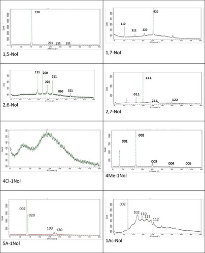
Figure 9. Crystal packing.
The experimental X-ray patterns obtained with the HZG-4 diffractometer and visualized with the graphic interface of the Dronek software were compared with the theoretical diffractograms calculated with the Diamond Version 3.2k and Mercury 3.8 (Build RC2) software on the basis of the known crystal structure from the crystallographic database. It allowed to indicate the reflexes of the diffraction patterns of the layers and to determine the arrangement of the layer molecules in relation to the substrate. The application of the Scherer formula also works for the materials made of nanometer-sized grains [Citation37–39]. A computer simulation with the use of the Diamond program is required in this case. The quantitative assessment of the mean size of the grains forming the tested layers was determined using the Scherrer equation [37].
Additionally assessment of the maximum size of the grains in 4Cl-1Nol, the layers of which showed a very diffused diffraction pattern, was possible in the manner shown in [Citation39]. Sizes of grain can be estimated of an order of (0.15 ± 0.09) µm. The layers of materials from class 1, i.e. with two -OH substituents, showed larger grain diameters between 4 µm and 8 µm, while polycrystalline layers of class 2 materials (except for amorphous layers 4Cl −1-Nol) showed a smaller diameter with a value close to 3 µm.
However, for derivatives 1,7-Nol, 2,6-Nol belonging to class 1 characterized with high level of drift mobility the space of two C atoms connected two benzene rings is participated in HOMO orbital. The higher level of drift mobility for derivatives 1Ac-Nol, 4Cl-1Nol and 1,5-Nol is not directly related to the distribution of the HOMO orbital, but is most probably associated with the occurrence of specific intermolecular interactions.
XPRD measurements showed that only the 4Cl-1Nol layers were obtained as amorphous and the layers obtained for the other studied naphthalene derivatives were polycrystalline. The crystal structure of studied compounds reveals the monoclinic or orthorombic system ( and ). Based on the knowledge of the unit cell volume V, the number of molecules in the cell Z and assuming that each molecule can provide one charge carrier, the effective density of states Nv can be estimated using the formula [Citation4]:
(3.2)
(3.2)
The value of Nv obtained in this manner is given in the and . Such a quantitative approximation allows to assess the maximum number of charge carriers that can occur in the system.
All the layers of studied naphthalene derivatives have relatively low specific conductivity () except for 1,5-Nol and 4Cl-1Nol, being respectively in the ranges (7.1·× 10−12−2.4·× 10−10) Sm−1 and (8.4·× 10−12 − 1.0·× 10−10) Sm−1. 1,5-Nol forms crystalline layers, while 4Cl-1Nol forms amorphous layers. Nevertheless, the layers of both compounds reveal high specific conductivity. It should be noted that in the case of volume crystals of 4Cl-1Nol and of 1,5-Nol, the presence of pi-stacking in their crystal packing have been shown. That phenomenon is favorable for increased electrical conductivity [Citation8, Citation31–33].
The and 8 show the determined values of the drift mobility and the Einstein mobility for the layers of studied naphthalene derivatives calculated as shown in [Citation43, Citation44]. In the class 1 of studied naphthalenes, the highest concentration of free carriers nf equals to (7.0 ± 1.1)·× 1011 cm−3 is registered for 1,7-Nol and (5.0 ± 0.8)·× 1011 cm−3 for 1,5-Nol. Maximally free carriers’ concentration, which can be obtained as a result of thermal emission, n0 () is also greater for 1,7 Nol than for 1,5-Nol. Both derivatives exhibit a relatively high value of drift mobility (4.0 ± 1.6)·× 10−4 cm2/Vs and (3.2 ± 1.3) ×·10−4 cm2/Vs, respectively.
It is clearly seen that the value of the electrical parameters of the tested layers of the other naphthalenes from the class 1 () are primarily determined by the substitution of the -OH group in position 1.
In the class 2 of tested naphthalenes, the highest concentration of free carriers nf found in the layers of 1Ac-Nol was (4.3 ± 1,3)·× 1011 cm−3 and in the layers of 4Cl-1Nol was (2.2 ± 0,8)·× 1011 cm−3. The layers of derivative 1Ac-Nol showed the highest drift mobility value (3.0 ± 1.2)·× 10−3 cm2/Vs while for 4Cl-1Nol the value of drift mobility was in the magnitude of (6.3 ± 2.5)·× 10−4 cm2/Vs. The high mobility value for 4Cl-1Nol can be connected with the occurrence of pi-stacking in the vicinity of each molecule (despite the fact that the layers were amorphous). Conversely, the high value of drift mobility for the 1Ac-Nol derivative may possibly be caused (see subsection 2.5) by easier charge carrier transport between molecules of this compound.
According to the Marcus model, electron transfer between adjacent molecules can be considered as a coupling problem between two surfaces of diabatic potential. The value of this coupling determines the value of the transfer integral Jij. According to the Marcus model, charge transfer should occur without activation energy, if the following condition is met [Citation41]:
(3.3)
(3.3)
where Er-reorganization energy.
This condition is fulfilled for all tested naphthalene derivatives. The theoretical calculation of the value of mobility of charge carriers using the parameters calculated from the Marcus–Hush model is possible because of the Einstein relationship linking the diffusion coefficient with this mobility [Citation4, Citation8, Citation9, Citation11, Citation26]. This mobility is named here as Einstein mobility and is calculated with the equation
(3.4)
(3.4)
where D diffusion coefficient for charge transfer, e- the charge of charge carrier, kB-Boltzmann constant, T-the Kelvin temperature.
To calculate this value, it is necessary to estimate the diffusion constant of charge carriers D [Citation9, Citation11]. If the average value of the charge carrier transfer rate Kij between two molecules is known then based on this results from [Citation45, Citation48] the diffusion constant D needed for calculation of the mobility of holes can be estimated:
(3.5)
(3.5)
where rij is the distance between centroids (centers of mass) of the molecule under study i and the neighboring molecule j, Ni is the number of the dimers consisted from this molecule and their neighbors, M is the number of independent molecules in the asymmetric unit, Ke+ is averaged chargé transfer rate between two molecules in the dimers, L is effective length of the charge transfer in the single jump, n is dimensionality of transport process (we assume here, n = 3), LK is coordination number of the ith molecule due to the possibility of the direct charge carrier transfer between molecules (we assume LK = 6). Parameter L can be approximated as an average distance between centroids for the dimers built from neighboring molecules. Probability Pij, of the chargé carrier jumping between neighboring molecules i and j in the dimer is related to the charge transfer integral Jij by the relation [Citation3]:
(3.6)
(3.6)
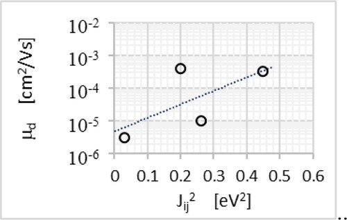
Using approximation (3.5) with assume that the parameter L about 4 Å [Citation9], and using the calculated values of charge transfer rate Kij+ which are for the studied compounds are in the range from 5.4·× 1013 Hz to 1.5·× 1015 Hz calculated before modifying the value of transfer integral with the exp (–2 rij/L) [Citation39] parameter, the value of which can be estimated at 0.8 [Citation45]; we obtain, based on the formula (3.4) (3.5) and (3.6), that the mobility of holes is in the range from 3.7·× 10−2 cm2/Vs to 95·× 10−2 cm2/Vs. Estimated on the basis of experimental data the Einstein mobility ( and ) are in the range of (1.2 ± 0.6)·× 10−2 cm2/Vs – (25 ± 10) ×·10−2 cm2/Vs. The above as well as the fact that the value of drift mobility is less than × 10−2 cm2/Vs suggest, that for the studied naphthalene derivatives we have the case of hopping transport. With such a transport, according to Marcus–Hush theory, the mobility of charge carriers should depend on the reorganization energy, Er, the Jij transfer integral and Ke hopping rate. This nature of the relationship suggests diagrams in the . The good coincidence between drift mobility and reorganization energy for the derivatives of derivatives of class 2 is observed. There is a strong relationship between hopping rate and drift mobility.
Figure 10. The dependence of drift mobility on reorganization energy for the derivatives of the class 1, (a), and of derivatives of the class 2, (b).
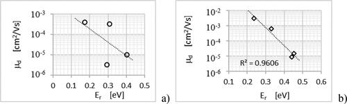
Figure 11. The drift mobility dependence on the charge transfer rate for the derivatives of the class 1, (a), and of derivatives of the class 2, (b).
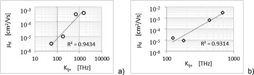
Figure 12. The drift mobility dependence on the square of the charge transfer integral for the derivatives of the class 1, (a).
The results of DFT calculations show, that is possible to reduce the energy of reorganization in the case of 1,7-Nol molecule. Substitution with two hydroxyl groups at the 1.7 position, i.e. on one side of the long axis of the naphthalene backbone, reduces reorganization energy from (0.19 ± 0,05) eV for naphthalene to (0.17 ± 0,04) eV (ΔEr = 0.02 eV). for 1.7-Nol. The value of the charge transfer integral Jij shows an increase from the level (0.37 ± 0.18) eV for naphthalene to (0.45 ± 0.21) eV for 1,7-Nol (ΔJij = 0.08 eV). In result, the calculated hole transfer rate for 1,7-Nol (1.5 ± 1.1)·× 1015 Hz) is the highest among the naphthalene derivatives studied here and is almost twice as high as that for unsubstituted naphthalene (8.9 ± 6.7)·× 1014 Hz.
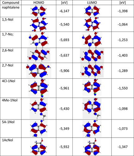
For the 1,7-Nol and 2,7-Nol derivatives the estimation of Einstein drift mobility (see and 8) is consistent with the measurement results in the range of measurements errors. The chemical stability of the layers under environmental conditions is a significant limitation on the use of organic materials. Resilience to oxygen and moisture during the transport of charge carriers is primarily associated with the energy values of HOMO and LUMO levels [Citation48, Citation49]. Hole transporting materials in which the energy value of the HOMO level is below −5 eV is considered sufficiently stable to produce organic electronics [Citation48]. All the naphthalene derivatives studied in this paper fulfill this condition. The energy of the HOMO level calculated for molecules in the gas phase is in the range from −5.430 eV for 4Me-1Nol to −5.906 eV for 2,7-Nol.
It is observed () that for compounds with low mobility of holes, there is absence of HOMO orbitals spread around two C atoms connected two benzene rings of naphthalene skeleton. This note applies inter allia to 2,7-Nol, 4Me-1Nol and 5 A-1Nol.
Figure 13. HOMO and LUMO for tested compounds and nonsubstituted naphthalene.
The analysis of the results of the mobility values belonging to the class 1 of the compounds ( and ) shows that the values of the overlap integral has a very weak effect on the value of Einstein's mobility both when calculations were based on the measurements of the trap fill factor in SCLC mode θ and when calculated as a result of the DFT analysis. In turn, the values of the drift mobility in the case of 1.5-Nol and 2.7-Nol depend on the value of the overlap integral Jij. For both of these compounds, despite the same reorganization energy, the drift mobility value is different by two orders of magnitude. However, within the error limits, we do not observe the reorganization energy influence on the obtained Einstein mobility values in the case of these two materials.
With comparable values of the overlap integral Jij, but with a two-fold difference in the value of the reorganization energy Er, we observe that the difference in the drift mobility value is almost 1.5 of the order of magnitude.
In the case of the derivatives shown in (the class 2 of compounds) it is difficult (within the error limits) to clearly define the nature of the dependence of Einstein mobility and drift mobility on the reorganization energy parameter Er, the overlap integral Jij and the charge transfer rate Ke.
Among the remaining derivatives, the peri-naphthalene derivative, i.e. 1Ac-Nol is distinguished, for which the value of the reorganization energy Er is relatively small, the value of the overlap integral Jij is the lowest and the value of the charge transfer rate Ke is relatively high. For this naphthalene derivative, the value of Einstein's mobility obtained from DFT calculations, µED, is, within the error limits, comparable with the Einstein mobility determined for the remaining naphthalene derivatives. However, this compound differs from other materials with its high value of drift mobility.
4. Conclusions
The experimental results and quantum-chemical calculations indicate the hopping nature of the hole transport in the examined materials.
The position of substitution determines the electronic properties of the tested naphthalenes double-substituted with -OH group ().
Modification of naphthalene derivatives should go in the direction of reducing the energy of reorganization of the molecule and increasing the transfer rate of charge carriers in order to achieve greater drift mobility of charge carriers.
Modification of dihydroxyl molecules of naphthalene derivatives, possessing both classes in the alpha position, increases the proportion of contacts type C···C and is accompanied by a decrease in the ratio (% C · H)/(% C · C) which causes pi-stacking nature of particle arrangement.
Studied materials are useful for applications as p-type semiconductors due to the low HOMO value (<–5 eV). The high LUMO value (from –1.567 eV to –1.066 eV) causes low chemicals resilience of these materials to direct action of oxygen in electron conduction conditions. They can be useful for application inside multilayered structures.
Acknowledgments
We express gratitude to Piotr Sawicki from the Department of Structural and Material Research IChOŚB WM-P UJD Częstochowa for performing XPRD measurements. The authors are grateful to the Lodz University of Technology for granting access to computing infrastructure built as part of PLATON projects no. POIG.02.03.00-00-028/08 - U3 and MAN-HA campus calculation service no. POIG.02.03.00-00-110/13 - "Implementation of critical services with a high level of reliability in MANs." The calculations mentioned in this paper are performed using TUL Computing & Information Services Center infrastructure.
References
- M. Borsenberger and D. S. Wiss, Organic Photoreceptor for Imaging Systems (Marcel Dekker, New York, 1993).
- J. Roncali, P. Leriche, and P. Blanchard, Adv. Mater. 26 (23), 3821 (2014). doi:10.1002/adma.201305999
- J. E. Campbell, J. Yang, and G. M. Day, J. Mater. Chem. C 5 (30), 7574 (2017). doi:10.1039/C7TC02553J
- M. Pope and C. E. Swenberg, Electronic Processes in Organic Crystals and Polymers, 2nd ed. (Oxford Science Publications, Oxford, 1999).
- H. P. Diogo et al., J. Am. Chem. Soc. 124 (9), 2065 (2002). doi:10.1021/ja012541+
- Y. Yang, E. R. Davidson, and W. Yang, Proc. Natl. Acad. Sci. USA 113 (35), E5098 (2016). doi:10.1073/pnas.1606021113
- C. Lee and K. Sohlberg, Chem. Phys. 367 (1), 7 (2010). doi:10.1016/j.chemphys.2009.10.005
- D. M. Carlton, D. K. McCarthy, and R. H. Genz, J. Phys. Chem. 68 (9), 2661 (1964). doi:10.1021/j100791a047
- A. Datta, S. Mohakud, and S. K. Pati, J. Chem. Phys. 126 (14), 144710 (2007). doi:10.1063/1.2721530
- K. Yoshizawa, Acc. Chem. Res. 45 (9), 1612 (2012). doi:10.1021/ar300075f
- W.-Q. Deng and W. A. Goddard, III, J. Phys. Chem. B 108 (25), 8614 (2004). doi:10.1021/jp0495848
- D. Glossman-Mitnik et al., J. Mol. Struct.: THEOCHEM 863 (1–3), 99 (2008). doi:10.1016/j.theochem.2008.05.031
- I. A. Fedorov, Y. N. Zhuravlev, and V. P. Berveno, Phys. Chem. Chem. Phys. 13 (13), 5679 (2011). doi:10.1039/c0cp02200d
- M. J. Frisch, Jr. et al., Gaussian 09, Revision A.02 (Gaussian, Inc., Wallingford, CT, 2016).
- D. H. Spielberg, A. I. Korn, and A. C. Damask, Phys. Rev. B 3 (6), 2012 (1971). doi:10.1103/PhysRevB.3.2012
- K. Hannewald and P. A. Bobbert, AIP Conf. Proc. 772, 1101–1102 (2005).
- N.-E. Lee et al., Phys. Rev. B 97, 115203–1 (2018).
- H. F. Clausen et al., New J. Chem. 34 (2), 193 (2010). doi:10.1039/B9NJ00463G
- P. Mark and W. Helfrich, J. Appl. Phys. 33 (1), 205 (1962). doi:10.1063/1.1728487
- J. Dacuña and A. Salleo, Phys. Rev. B 84 (19), 195209 (2011). doi:10.1103/PhysRevB.84.195209
- V. Mikhelashvili and G. Eisenstein, J. Appl. Phys. 89 (6), 3256 (2001). doi:10.1063/1.1349860
- J. Sworakowski and K. Pigoń, J. Phys. Chem. Solids 30 (3), 491 (1969). doi:10.1016/0022-3697(69)90004-3
- R. A. Marcus, Rev. Mod. Phys. 65 (3), 599 (1993). doi:10.1103/RevModPhys.65.599
- N. S. Hush, J. Chem. Phys. 28 (5), 962 (1958). doi:10.1063/1.1744305
- H.-S. Ren et al., J. Phys. Chem. A 117 (33), 8017 (2013).
- D. Mendels and N. Tessler, J. Phys. Chem. C 117 (7), 3287 (2013). doi:10.1021/jp311577w
- M. Rossi and K. Sohlberg, J. Phys. Chem. C 113 (16), 6821 (2009). doi:10.1021/jp8086978
- B. Marciniak, Acta Crystallogr. C Cryst. Struct. Commun. 63 (4), o252 (2007). doi:10.1107/S0108270107009109
- V. K. Belskii et al., Zhurnal Strukturnoi Khimii 31 (5), 116 (1990).
- E. Rozycka-Sokolowska, B. Marciniak, and V. Pavlyuk, Acta Crystallogr. E Struct. Rep. Online 61 (1), o114 (2005). doi:10.1107/S1600536804032453
- B. Marciniak and E. Różycka-Sokołowska, Acta Crystallogr. C Cryst. Struct. Commun. 65 (12), o630 (2009). doi:10.1107/S0108270109047556
- E. Rozycka-Sokolowska and B. Marciniak, Acta Crystallogr. C 65 (Pt 5), o207 (2009). doi:10.1107/S0108270109010063
- E. Rozycka-Sokolowska and B. Marciniak, Acta Crystallogr. C Cryst. Struct. Commun. 65 (11), o565 (2009). doi:10.1107/S0108270109038694
- B. Marciniak, Acta Crystallogr. E Struct. Rep. Online 63 (3), o1311 (2007). doi:10.1107/S1600536807006952
- S. K. Wolff et al., Crystal Explorer 3.1 (University of Western Australia, Perth, 2012).
- S. A. Gandhi et al., Mol. Cryst. Liq. Cryst. 708 (1), 98 (2020). doi:10.1080/15421406.2020.1811023
- D. Pop et al., Materials 14 (13), 3556 (2021). doi:10.3390/ma14133556
- A. R. Stokes and A. J. C. Wilson, Math. Proc. Camb. Phil. Soc. 38 (3), 313 (1942). doi:10.1017/S0305004100021988[Mismatch]
- A. O. Bokuniaeva and A. S. Vorokh, J. Phys.: Conf. Ser. 1410 (1), 012057 (2019). doi:10.1088/1742-6596/1410/1/012057
- M. Ansari-Rad, Y. Abdi, and E. Arzi, J. Phys. Chem. C 116 (5), 3212 (2012). doi:10.1021/jp207907b
- E. A. Silinsh et al., Chem. Phys. 198 (3), 311 (1995). doi:10.1016/0301-0104(95)00151-D
- H. Yamagata et al., J. Chem. Phys. 134 (20), 204703 (2011). doi:10.1063/1.3590871
- H. Fritzsche, Diam. Relat. Mater. 14 (2), 74 (1982).
- S. Kania and J. Kuliński, Sci. Bull. Phys. 37, 65 (2016).
- E. Marfo-Owusu and A. L. Thompson, Acta Crystallogr. Sect. E Struct. Rep. Online 69 (Pt 11), o1655 (2013). doi:10.1107/S1600536813026731
- A. Köhler and H. Bässler, J. Mater. Chem. 21 (12), 4003 (2011). doi:10.1039/C0JM02886J
- A. Winkler, Surf. Sci. 652, 367 (2016). doi:10.1016/j.susc.2016.02.015
- T. Xu et al., Phys. Chem. Chem. Phys. 19 (22), 14453 (2017). doi:10.1039/c7cp01534h
- K. Takimiya et al., Sci. Technol. Adv. Mater. 8, 273 (2007). doi:10.1016/j.stam.2007.02.010