
ABSTRACT
We develop a nanosecond grating imaging (NGI) technique to measure in-plane thermal transport properties in bulk and thin-film samples. Based on nanosecond time-domain thermoreflectance (ns-TDTR), NGI incorporates a photomask with periodic metal strips patterned on a transparent dielectric substrate to generate grating images of pump and probe lasers on the sample surface, which induces heat conduction along both cross- and in-plane directions. Analytical and numerical models have been developed to extract thermal conductivities in both bulk and thin-film samples from NGI measurements. This newly developed technique is used to determine thickness-dependent in-plane thermal conductivities (κx) in Cu nano-films, which agree well with the electron thermal conductivity values converted from four-point electrical conductivity measurements using the Wiedemamn–Franz law, as well as previously reported experimental values. The κx measured with NGI in an 8 nm x 8 nm GaAs/AlAs superlattice (SL) is about 10.2 W/m⋅K, larger than the cross-plane thermal conductivity (8.8 W/m⋅K), indicating the anisotropic thermal transport in the SL structure. The uncertainty of the measured κx is about 25% in the Cu film and less than 5% in SL. Sensitivity analysis suggests that, with the careful selection of proper substrate and interface resistance, the uncertainty of κx in Cu nano-films can be as low as 5%, showing the potential of the NGI technique to determine κx in thin films with improved accuracy. By simply installing a photomask into ns-TDTR, NGI provides a convenient, fast, and cost-effective method to measure the in-plane thermal conductivities in a wide range of structures and materials.
Introduction
With the development of electronics with micro-/nanoscale size and high power density, thermal management has become a crucial problem. Vigorous efforts have been made to measure the thermal conductivity in micro-/nanoscale electronic materials, such as thin films [Citation1–Citation3], nanowires [Citation4, Citation5], superlattices (SLs) [Citation6–Citation8], and 2D semiconductors [Citation9, Citation10]. Among the many approaches developed in recent decades for thermal conductivity measurement in micro-/nanostructures, the most commonly used include the 3ω method [Citation1, Citation2], time-domain thermoreflectance (TDTR) [Citation3, Citation11, Citation12], Transient Thermal Gratings (TTG) [Citation13], Raman spectroscopy [Citation14–Citation16], and the four-probe thermal measurement method [Citation17]. The 3ω method provides accurate measurement of cross-plane thermal conductivity, especially in bulk materials and low- dielectric films. It is also possible to observe lateral thermal transport using the 3ω method in specific structures, such as a long suspended film, although the overall sensitivity of the measurement is less satisfactory and the fabrication of these structures is challenging [Citation2]. TDTR employs pulsed lasers (femto-, pico-, or nanosecond) to measure the differential reflectivity change at the sample surface due to pump laser heating and offers the experimental advantages of high spatial resolution and high sensitivity to thermal interface resistance. For most applications of TDTR, one-dimensional heat transfer is generally assumed, as the thermal penetration depth of a short laser pulse is much smaller than that of the laser spot size [Citation3]. Femtosecond TDTR system with a scanning probe beam is utilized to determine the in-plane thermal conductivity in silicon [Citation18] and graphite [Citation19], which is rather time consuming. For the TTG technique, TTG is formed by two crossing pump beams, which can be generated conveniently with a specially designed phase mask [Citation13, Citation20]. A probe beam is used to monitor the change in physical properties induced by TTG. Detection of TTG can be achieved by recording the first-order diffracted probe beam [Citation21, Citation22], surface displacement due to thermal expansion [Citation13], or temperature-induced probe reflectivity change [Citation23]. Heterodyne detection is usually used to amplify the first-order diffracted probe signal of either transmission or reflectance [Citation20]. TTG has been utilized to measure the in-plane thermal conductivities in Si [Citation24], GaAs [Citation25], GaAs/AlAs SL [Citation8], and PbTe [Citation26]. Metal nano-heaters fabricated with nano-lithography on a sample surface are also used to introduce lateral thermal transport, where a pump beam heats the metal grating and the diffracted probe beam from the heated metal grating is collected as the signal [Citation27–Citation29], similar to that in TTG. The measured thermal conductivity values show a strong dependence on the size of metal heaters, which indicates a transition from non-diffusive to diffusive thermal transport regimes. However, in nature these metal gratings are invasive to the sample. Raman spectroscopy has been reported to successfully measure the in-plane thermal conductivity in ultrathin films [Citation11] and 2D materials [Citation14, Citation16], by detecting Raman peak shifts due to thermal expansion and bond softening as a function of laser heating power. Extracting thermal conductivity from Raman measurements is relatively simple, when a proportional relationship can be assumed between the temperature and Raman peak shift. However, accurate calibration of Raman peak shift over a wide range of temperatures is necessary to achieve a satisfactory uncertainty of the measured thermal conductivity, and the materials to be measured must be Raman active and sensitive enough. The four-probe thermal measurement method can measure intrinsic thermal conductance and thermal contact resistance in individual nanostructures [Citation4, Citation17, Citation30]. This method consists of four suspended metal lines that function as both resistive heaters and thermometers, with the sample bridging across the four micro-fabricated metal lines [Citation17]. Intrinsic thermal properties can be measured very accurately with the four-probe method, but a new device needs to be fabricated for each sample, which could be very challenging.
In this work, we implement a grating imaging technique into ns-TDTR in order to measure the in-plane thermal conductivity and name it as nanosecond grating imaging (NGI). A permanent grating image is generated on the sample surface using a photomask, and then a thermoreflectance signal containing thermal transport information in both in-plane and cross-plane directions is collected. The experimental setup of NGI is very simple because we monitor the temperature-induced probe reflectivity change instead of diffraction. Recently, we implemented the same grating imaging technique into our femtosecond pump-probe spectrometer to detect carrier diffusion in graphene [Citation31] and GaAs/AlAs SLs [Citation32]. Our new technique is developed based on ns-TDTR due to its several advantages compared with an fs-TDTR. First, the ns-TDTR system is a real time-resolved system to observe surface temperature, but much cheaper, costing only about 1/10 of the fs-TDTR system. Second, without a mechanical delay-stage to create time delay and a lock-in amplifier for data acquisition, ns-TDTR allows much faster measurement because a fast averaging process can be conducted directly with an oscilloscope. Third, data analysis with the ns-TDTR system is much simpler than in most materials of interest. After tens of nanoseconds, the complicated electron-phonon nonequilibrium processes already finishes. Heat conduction models are also established to extract thermal conductivities from the experimental data of the NGI technique. This new approach is utilized to measure the in-plane conductivities in Cu nano-films on Si substrate and an 8 nm x 8 nm GaAs/AlAs SL.
Experimental
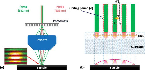
A Nd:YAG pulsed laser (532 nm, 15 ns pulse width) is used as the pump and a He-Ne laser (632 nm, cw) as the probe. A 10x objective lens is used to focus both the pump and probe beams onto the sample surface, and the reflected probe beam is collected by a silicon photodetector (Thorlabs, PDA10A). For standard ns-TDTR, the pump spot diameter (1/e2) is about 1 ~ 2 mm, and the probe diameter is about 180 µm. This large pump/probe spot size ratio ensures that cross-plane thermal transport is dominant and that a simple 1-D thermal conduction model can be used to extract the cross-plane thermal conductivity. To measure the in-plane thermal conductivity, a grating imaging technique is incorporated into the standard ns-TDTR setup. This technique is called NGI, as illustrated in . A photomask with periodic metal strips patterned on a transparent dielectric substrate is placed before the objective lens. Collinearly aligned pump and probe lasers pass through the photomask, and grating images from both pump and probe (transmitted and diffracted from the photomask) are generated by the objective lens and overlap on the sample surface, as shown in . (See supplementary information for images of grating formed on the sample surface.) The grating period (λ) is determined by the slit size on the photomask and the magnification factor of the objective lens (e.g. ). The periodically modulated pump laser generates thermal grating along the sample surface, which induces heat flow along both in-plane and cross-plane directions. Because the probe beam is modulated in the same way as the pump, both the in-plane and cross-plane heat flows will lead to decay of the reflection change. By monitoring the reflected probe beam, both in-plane (
) and cross-plane (
) thermal conductivities can be extracted. However, to simplify the analysis of NGI measurements, in this study, the
value is either predetermined with standard ns-TDTR or obtained from the literature. For NGI, the pump diameter is 530 µm and the probe diameter is also about 180 µm.
Figure 1. (a) Schematic diagram of the experimental setup of the grating imaging technique; (b) in-plane and cross-plane heat flow generated by the pump and detected by the probe.
A thermal diffusion model considering a periodic heating source on the sample surface is developed to fit the experimental data and to extract thermal conductivity:
As illustrated in , each fringe of our grating image has a rectangle shape, which is a superposition of several sinusoidal waves. The profile of the periodic heating source can be expressed as follows:
where is the temporal shape of the Gaussian pump pulse.
In bulk samples, the surface temperature can be solved analytically from Eq. 1 & 2 in the frequency domain [Citation13] (see the supplementary information for details of derivation for Eqs. 3~ 5):
where is the laser fluence,
is density,
is specific heat,
is the cross-plane thermal diffusivity,
is the in-plane thermal diffusivity, and
is the position along the sample surface. Within the temperature range where probe reflectivity change is linearly proportional to the change in surface temperature, i.e.
, the detected change in probe reflectivity is an integrated value within the whole probe spot:
, where
is the probe response function to temperature change. In our case,
is the product of a Gaussian function and a square function. Since our probe spot size is much smaller than that of the pump, we can assume that pump fluence across the probe spot is uniform, so that the final solution for bulk materials can be simplified as follows:
The solution of Eqs. 1 and 2 is much more complicated in multilayer samples, and can be expressed as [Citation13]
where ,
,
,
.
Results and discussion
In this study, we measured the in-plane thermal conductivity in two different types of samples, GaAs/AlAs SL and Cu nano-films on Si substrate, representing the bulk and layered structures, respectively. First we determine the κx values of Cu nano-films and compare them with the literature values, as examples to validate the NGI technique, and then we study the anisotropic thermal conductivities in GaAs/AlAs SL with ns-TDTR and NGI.
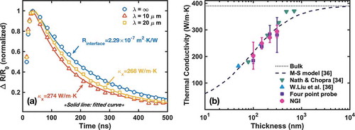
Cu nano-films with four different thicknesses (100, 150, 220, and 310 nm, measured by a profilometer; Veeco Dektak 6M) are evaporated onto a SiO2 (300 nm)/Si substrate to perform ns-TDTR and NGI measurements. We assume that the reflectivity change of the Cu film at probe wavelength (632 nm) has a linear relation with temperature. We measured the reflectivity of our Cu film at different temperatures and obtained a dR/dT ~2.8 × 10⁻⁴ K−1 (see supplementary information). Optical penetration depth of the pump (523 nm) in Cu is 33 nm, so we can assume that all the heat is absorbed by the Cu layer. Electron-phonon coupling time for Cu is less than 30 picoseconds, which should not affect our experiment [Citation33]. shows the results for the 220-nm-thick Cu nano-film, for which two different grating periods (10
and 20
) are used, and the temperature rise at the sample surface is estimated to be lower than 9 K. Because the pump and probe beams are modulated in the same way, the probe beam only senses the area heated by the pump (green lines in ). The change in probe signal reflects the temperature dynamics of these heated lines. For comparison, results from the ns-TDTR measurement (
) are also plotted in . In the ns-TDTR measurement, only thermal conduction along the cross-plane direction is important, whereas in NGI measurements, in-plane thermal conduction also takes place, and hence a faster decay of surface reflectivity is observed in the NGI experiments. Moreover, compared with a larger grating period (
20
), the decay is faster using a smaller grating period (
10
). Since the pump size and laser power do not change when using different grating periods, and we can assume uniform pump fluence in the probed area, the pump fluence within the heated lines (green lines in ) is the same for all the grating periods. The temperature rise (TH) in the heated lines is the same and the temperature in the unheated lines is at room temperature (TL). The heat flux density induced by this temperature gradient is:
. With smaller grating period, qx is larger, which will lead to a faster decay of the temperature gradient, e.g. it will take less time for temperature across the grating to become uniform.
Figure 2. (a) Experimental and fitting results for Cu 220-nm-thick nano-film measured by ns-TDTR (λ = ∞) and NGI with grating periods of 10 μm and 20 μm; (b) comparison of κx of Cu nano-films measured by NGI with four-point probe results as well as reference values. (Error bars indicate a standard deviation based on five measurements at different locations on the sample.)
Based on Eq. 5, there are five unknown parameters here: cross-plane thermal conductivity and in-plane thermal conductivity of Cu nano-films and Si (), and interface resistance (
). For Si, bulk thermal conductivity is used,
. The SiO2 layer is treated as part of the interfacial resistance. For ns-TDTR, when
is bigger than 100
, the simulation curves do not change, because heat diffusion in a Cu layer is too fast to be captured at the nanosecond scale. In our fitting process, thickness-dependent
values from the literature are used for cross-plane thermal conductivity (
for 100, 150, 220, and 310 nm, respectively) [Citation34] . Interface resistance values for each sample are obtained from ns-TDTR measurement and determined as
and
for the 100, 150, 220, and 310 nm films, respectively. There is only one fitting parameter remaining, the in-plane thermal conductivity of Cu (
). The in-plane thermal conductivity for Cu of 220 nm thickness is determined as 274 W/mK and 268 W/mK using 10 μm and 20 μm grating periods, respectively, after optimizing the least-squares fitting of the experimental data with Eq. 5. With different grating periods, the obtained values of thermal conductivity vary by about 2%, which confirms the consistency of measurements with NGI. The κx values for all four Cu samples with different thicknesses are plotted as red dots in . To validate the NGI results, we also measured the electrical conductivity of the same Cu samples using a four-point collinear probe method [Citation35]. Four electrical probes are arranged collinearly at the center of each sample, with a spacing of 1 mm between probe tips. For each four-point probe measurement, the results are averaged over three probe orientations and collected using a Micromanipulator Co. 6200 probe station and Agilent B1500 parameter analyzer. The sheet resistance is calculated from the as-measured resistance using standard four-point probe geometry correction factors, and then converted to electron thermal conductivity via the Wiedemann–Franz (W-F) Law, as plotted in (purple squares). In metals [Citation36], electrons are the major heat carriers and electrical conductivity is linked to electron thermal conductivity by the W-F Law: κ/σ = LT, where κ is the thermal conductivity,
is the electrical conductivity,
is the Lorenz number, and
is temperature. It is reported that the Lorenz number depends on temperature and thickness [Citation36], and the Lorenz numbers applied here to derive κx from the four-probe measurements are obtained by the interpolation of published data. The triangles shown in represent the κx values for Cu nano-films previously reported by W. Liu et al. (upper triangle) using Joule heating and electrical resistance thermometry in suspended micro-fabricated structures [Citation36] and by P. Nath and K.L. Chopra (lower triangle) using the steady-state method with a Kanthal heater and thermocouples [Citation34]. It can be concluded that the results from NGI measurements are consistent with those of the electrical conductivity measurements as well as with the reported values in the literature. In , the κx values of the Cu nano-films show an obvious increasing trend with film thickness, which can be explained by electron scattering at the grain boundaries. The electrical and thermal resistivities of the Cu films depend on the characteristic length (film thickness and/or width, or grain size). When this characteristic length is comparable to or smaller than the electron mean free path (MFP) in Cu, electron scattering at the grain boundaries dominates and the grain size becomes an important parameter [Citation37]. Mayads and Shatzkes reported that the electrical resistivity of thin metal films is controlled by electron scattering at the grain boundary and the film surface and established a model (M-S model) considering a specular reflection parameter of electrons at the film surface and the electron reflection coefficient at the grain boundaries [Citation38]. According to the M-S model, in thinner films the mean grain size decreases and more grain boundaries are present. Thus, the resistivity in thinner films is larger and the thermal conductivity is smaller. Thickness-dependent electrical resistivity of Cu films is calculated based on the M-S model and then converted to thermal conductivity with the W-F law [Citation36], shown as dashed line in . When the Cu film is very thick, such as over tens of microns, the thermal conductivity calculated with the M-S model converges to the bulk value. The κx values for Cu nano-films measured with NGI and four-probe techniques agree well with the theoretical predictions with the M-S model, which validates the usage of the NGI technique to measure in-plane thermal conductivity.
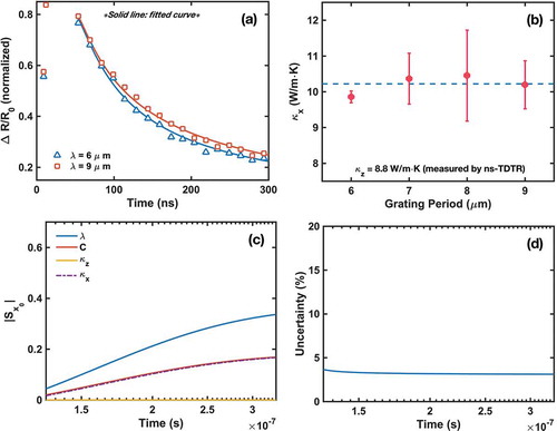
NGI is then utilized to measure the thermal conductivities of GaAs/AlAs SL, which is expected to possess anisotropic thermal conductivities along the in-plane and cross-plane directions [Citation8]. The two samples under test are cut from the same crystal, which has 219 periods, with each period consisting of 8 nm GaAs and 8 nm AlAs, epitaxially grown by MOCVD. One sample is coated with a 200-nm-thick aluminum film using e-beam evaporation to measure using ns-TDTR, and the obtained
value is 8.8
, consistent with the reported value [Citation8]. The other sample is uncoated and used to measure the
with NGI. Since the ambipolar diffusion coefficient of 10
in GaAs is much higher than the thermal diffusivity of 0.1
, the grating generated by photo-excited carriers should decay much faster than the thermal grating [Citation39, Citation40]. Within the time window used for our analysis (30 ~ 300ns), thermal diffusion should dominate. Experimental data before 30 ns is excluded to avoid effects from finite pump pulse duration. The thermal penetration depth within the analyzed time window (300 ns) is less than 2 µm in GaAs/AlAs SLs (
), much less than the sample thickness of 3.5 µm. As a result, the sample can be treated as a bulk crystal, and our thermal model for bulk crystal (Eq. 4) is appropriate to fit the experimental data, with properties averaged over GaAs and AlAs. Four grating periods (6, 7, 8, and 9 µm) were used in NGI measurements, and the experimental results with 6 and 9 µm grating periods are shown in . For each grating period size, a time constant
is defined to describe the characteristic decay time of the thermal grating. The time window for fitting should not be much longer than τ, which is 173, 236, 308, and 389 ns for grating period sizes of 6, 7, 8, and 9 um, respectively. Based on the considerations above, 300 ns is selected as the fitting time window. (In supplementary information, a fitting with 500 ns time window is also provided for comparison.) Similar to the Cu nano-films, the surface temperature of GaAs/AlAs SL relaxes faster when using a smaller grating period. Fitted in-plane thermal conductivity measured using all four grating periods is displayed in . The mean value of the measured
in GaAs/AlAs SL is around 10.2 ± 0.8
(reported as 11.4
) [Citation8]. The anisotropic thermal conductivity observed in SLs has been discussed extensively in the literature and two major causes have been proposed. i) The first is phonon scatterings at periodic interfaces [Citation41]; when the period thickness is comparable to or less than the phonon MFP, the size effect on thermal transport becomes dominant, referred to as ballistic thermal transport in each layer, and interface scattering affects thermal conductivity more significantly. ii) The second is modified phonon dispersion [Citation42], where the periodic structure in SL leads to phonon dispersion folding into a smaller first Brillouin zone, which opens mini phonon bandgaps at the zone center and zone edge and reduces phonon group velocity. All these factors greatly reduce the cross-plane thermal conductivity in SLs and give rise to anisotropy.
Figure 3. (a) Experimental and fitting results for an 8 nm x 8 nm GaAs/AlAs SL with grating periods of 6and 9
; (b) in-plane thermal conductivity results with different grating periods (error bars indicate a standard deviation based on five measurements at different locations on the sample); (c) sensitivity analysis of all parameters; (d) uncertainty for in-plane thermal conductivity measurement using NGI with a grating period of 7
.
When determining with the bulk model (Eq. 4), there are several important considerations: a) characteristic decay time of grating,
, the time for which the thermal grating persists, should be longer than the time window (t) chosen for analysis; and b) thermal penetration depth,
, the distance the thermal wave generated from the pump pulse can travel within the time window of analysis, should be less than the sample thickness. Thermal diffusivity is estimated by
using experimentally obtained thermal conductivity (
) values and the density (
and specific heat (
of the average values of GaAs and AlAs [Citation43].
Sensitivity analysis has also been conducted to assess the uncertainty of measurements with the NGI technique. The sensitivity to a parameter, , for a single material of interest and at a certain time is defined as:
[Citation12], which is estimated with the change of normalized temperature, when the parameter changes by ± 10% within the timescale of interest:
With the sensitivities to all the key parameters known, we can calculate the uncertainty of the measured in-plane thermal conductivity value as
where is the uncertainty of
measurement,
is the uncertainty of parameter
, and the summation is over all parameters of interest. The results of sensitivity analysis for GaAs/AlAs SLs are shown in , indicating that grating period is the most sensitive parameter, followed by in-plane thermal conductivity and heat capacity. The uncertainty of the grating period is caused by a fabrication accuracy of 250 nm (e.g.
). Literature values are used for GaAs and AlAs heat capacities and an uncertainty of 3% is assumed for this parameter. The uncertainty of in-plane thermal conductivity measurement using NGI is calculated as 3% when the measurement time is longer than 100 ns, as plotted in .
For layered structures, such as a thin film on a substrate, it is more complicated to determine the optimal experimental condition. Sensitivity studies have also been performed for Cu nano-films on Si substrate, in order to optimize the design of sample structures for in-plane thermal conductivity measurements using NGI. For 220 nm Cu film on SiO2 (300 nm)/Si substrate, parameters of interest include: the grating period (), thermal conductivities of Cu (
,
) and Si (
,
), heat capacities of Cu (
) and Si (
), Cu film thickness (
), and interface resistance (
) between Cu and Si (the 300 nm SiO2 layer considered as part of the interface resistance).
Results of the sensitivity analysis shown in indicate that the film thickness, Cu heat capacity, and interface resistance are the most sensitive parameters, followed by the grating period and in-plane thermal conductivity of Cu films. Uncertainty analysis provides information about how accurately the NGI technique can measure the in-plane thermal conductivity of Cu films, for which uncertainties from all parameters should be considered. The uncertainty of film thickness originates from thickness measurement and is estimated to be 1 nm (e.g. ). The uncertainty of the grating period is caused by a fabrication accuracy of 250 nm (e.g.
). The uncertainty of interface resistance is around 3.3%, estimated by the sensitivity analysis of ns-TDTR measurements with all related parameters, as shown in and . Literature values are used for Cu heat capacity, Si heat capacity, and Si thermal conductivity, and an uncertainty of 3% is assumed for those parameters. As shown in , the averaged value of the uncertainty of
is about 25%.
Figure 4. (a) Sensitivity analysis of all parameters for 220 nm Cu on Si measured with NGI; (b) uncertainty of measured with NGI; (c) sensitivity analysis of all parameters for 220 nm Cu on Si measured with ns-TDTR; (d) uncertainty of interface resistance measured with ns-TDTR.
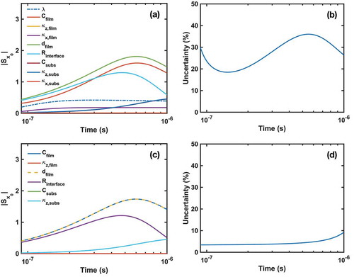
The obtained uncertainty of in the 220 nm Cu film using NGI is relatively high because sensitivity to other parameters, such as film thickness, heat capacity of thin film, and interface resistance, is larger than the sensitivity to
. To reduce the uncertainty of the measured
, the sample structure needs to be further optimized so that the heat transport is highly confined within the Cu film, which will increase the sensitivity to
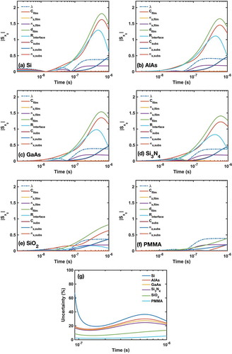
and decrease the sensitivity to Csub, κz,sub and Rinterface. Substrates with thermal diffusivity lower than Si may serve the purpose. Here, five widely used materials in electronics with a wide range of thermal diffusivities, AlAs (
~
), GaAs (
), Si3N4, (
), SiO2 (
), and PMMA (polymethyl methacrylate;
) [Citation44, Citation45], are selected for sensitivity analysis to study the effect of substrate on NGI measurement. presents the results of sensitivity analysis of 220 nm Cu films on various substrates, including Si. Only the parameters associated with substrates (Csub, κz,sub) change, and all other parameters (including interface resistance) remain the same as for the case of Si. A couple of interesting trends are observed here. (i) Sensitivities to κx,film and grating period λ remain the same for all substrates. (ii) Sensitivities to Cfilm and dfilm decrease on substrates with smaller diffusivities. When heat is highly localized within the film, the temperature in the film becomes more uniform across the film thickness and can only decay by heat transport along the in-plane direction. (iii) Sensitivity to Rinterface also decreases on substrates with smaller diffusivities. On SiO2 and PMMA substrates, it is even smaller than that of κx,film. It is reasonable because the effect from Rinterface becomes less important when heat transport mainly happens along the in-plane direction. shows the uncertainties of κx,film of the 220 nm Cu film on various substrates, calculated based on the sensitivity analysis presented in . The uncertainty of κx,film is greatly reduced on substrates with small thermal diffusivities, reaching around 10% on SiO2 and even below 5% on PMMA. The main reason is the sensitivity to κx,film becomes comparable to or even larger than the other parameters.
Figure 5. Sensitivity analysis for 220 nm Cu on various substrates: (a) Si; (b) AlAs; (c) GaAs; (d) Si3N4; (e) SiO2; and (f) PMMA. (g) Uncertainty of κx,film measurement in a 220 nm Cu film on various substrates.
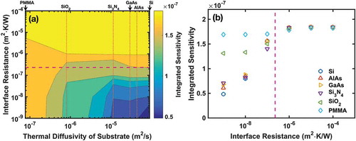
To consider the effects from substrates and Rinterface simultaneously, plots a contour mapping of sensitivity over substrate thermal diffusivity and Rinterface, where interface resistance is set to range from 10–9 to 10–4
. With small interface resistance, sensitivity has a strong dependence on substrate thermal diffusivity. When the interface resistance becomes large enough, the effect from substrate thermal diffusivity is less important. To have a better understanding of this trend, an integrated sensitivity parameter,
, defined as
, is shown in . It can be seen that the substrate effect is strong for Rinterface smaller than 10–8
but disappears for Rinterface larger than 10–6
. For the PMMA substrate, only a weak dependence on Rinterface is observed over the whole range. These results imply that Rinterface and substrate diffusivity play similar roles on heat transport in Cu films. With either a large enough Rinterface or small enough substrate thermal diffusivity, heat transport can be confined to along the in-plane direction in the Cu film, and hence reduce the uncertainty of the measured κx,film.
Figure 6. Sensitivity for Cu on various substrates with different interface resistance values. (Purple dashed horizontal line: used value for 220 nm Cu on Si.).
These sensitivity analyses suggest that choosing the proper substrate thermal diffusivity and film deposition method can significantly improve the accuracy of NGI measurement of in-plane thermal conductivity in thin films. To measure a highly thermal conductive film such as a metal, the substrate should be a dielectric material with small thermal diffusivity or a large thermal resistance should be present, so that thermal transport mainly occurs along the in-plane direction within the film. For our experiment, a thicker SiO2 layer between the Cu film and the Si substrate can provide a larger interface resistance and hence a higher sensitivity to κx,film. If the κx of the substrate is to be measured, a film with a relatively low thermal conductivity is needed as the top layer so that the heat can have enough time to penetrate the substrate. However, since the top film also needs to absorb laser energy and have a reflectivity sensitive to temperature change, it is not always easy to find the right material satisfying all the conditions, especially when the substrate has low thermal conductivity. The sensitivity analysis shows the potential of our NGI technique to measure κx in thin-film samples with improved accuracy. More experiments need to be conducted to validate this potential, which will be our future work. For the Cu film, we need to deposit new films for each substrate. However, it is not always necessary to tailor the sample. For example, we plan to apply this technique to measure 2D semiconductors, which stick to the substrate by van der Waal’s forces. The samples can be transferred to various substrates.
Conclusion
To summarize, we have developed a simple, fast, and low-cost NGI technique to measure the in-plane thermal conductivity in bulk and thin-film samples. The experimental setup of NGI is similar to that of standard ns-TDTR, but it employs a photomask to generate a thermal grating image onto the sample surface. The thermal grating produces a temperature gradient along the sample surface, which makes it possible to measure the in-plane thermal conductivities. The thickness-dependent in-plane thermal conductivities of Cu nano-films measured with NGI agree well with the electrical four-point probe measurements and the previously reported values. In-plane and cross-plane thermal conductivities measured in GaAs/AlAs SLs show strong anisotropy due to phonon folding and interface scattering. Sensitivity analysis suggests that the uncertainty of κx,film can be as low as 5% with careful selection of the proper substrate and interface resistance. This newly developed NGI technique overcomes some limitations of ns-TDTR. Together with ns-TDTR, this new technique can be used to determine in-plane and cross-plane thermal conductivities in a wide range of materials.
UMTE_A_1416713_Supplementary.docx
Download MS Word (1.9 MB)Acknowledgments
The authors also want to express their sincere appreciation to Dr. Maznev and Dr. Nelson at MIT for providing the GaAs/AlAs SL samples.
Supplementary material
Supplemental data for this article can be accessed publisher’s website.
Additional information
Funding
References
- D. G. Cahill, “Thermal conductivity measurement from 30 to 750 K: the 3ω method,” Rev. Scient. Instru., vol. 61, pp. 802–808, 1990. DOI: 10.1063/1.1141498.
- C. Dames, “Measuring the thermal conductivity of thin films: 3 omega and related electrothermal methods,” Annu. Rev. Heat Transfer, vol. 16, pp. 7–49, 2013. DOI: 10.1615/AnnualRevHeatTransfer.v16.
- C. A. Paddock and G. L. Eesley, “Transient thermoreflectance from thin metal films,” J. Appl. Phys., vol. 60, pp. 285–290, 1986. DOI: 10.1063/1.337642.
- D. Li, et al., “Thermal conductivity of individual silicon nanowires,” Appl. Phys. Lett., vol. 83, pp. 2934–2936, 2003. DOI: 10.1063/1.1616981.
- D. Li, Y. Wu, R. Fan, P. Yang, and A. Majumdar, “Thermal conductivity of Si/SiGe superlattice nanowires,” Appl. Phys. Lett., vol. 83, pp. 3186–3188, 2003. DOI: 10.1063/1.1619221.
- S.-M. Lee, D. G. Cahill, and R. Venkatasubramanian, “Thermal conductivity of Si–ge superlattices,” Appl. Phys. Lett., vol. 70, pp. 2957–2959, 1997. DOI: 10.1063/1.118755.
- S. T. Huxtable, et al., “Thermal conductivity of Si/SiGe and SiGe/SiGe superlattices,” Appl. Phys. Lett., vol. 80, pp. 1737–1739, 2002. DOI: 10.1063/1.1455693.
- M. N. Luckyanova, et al., “Anisotropy of the thermal conductivity in GaAs/AlAs superlattices,” Nano Lett., vol. 13, pp. 3973–3977, 2013. DOI: 10.1021/nl4001162.
- R. Yan, et al., “Thermal conductivity of monolayer molybdenum disulfide obtained from temperature dependent Raman spectroscopy.,” ACS Nano, vol. 8, pp. 986–993, 2013. DOI: 10.1021/nn405826k.
- X. Zhang, et al., “Measurement of lateral and interfacial thermal conductivity of Single- and Bilayer MoS2 and MoSe2 using refined optothermal Raman technique,” ACS Appl. Mater. Interfaces, vol. 7, pp. 25923–25929, 2015. DOI: 10.1021/acsami.5b08580.
- D. G. Cahill, “Analysis of heat flow in layered structures for time-domain thermoreflectance,” Rev. Scient. Instru., vol. 75, pp. 5119–5122, 2004. DOI: 10.1063/1.1819431.
- R. Garrelts, A. Marconnet, and X. Xu, “Assessment of thermal properties via nanosecond thermoreflectance method,” Nano. Microsc. Thermo. Eng., vol. 19, pp. 245–257, 2015. DOI: 10.1080/15567265.2015.1078425.
- O. W. Käding, H. Skurk, A. A. Maznev, and E. Matthias, “Transient thermal gratings at surfaces for thermal characterization of bulk materials and thin films,” Appl. Phys. Mater. Sci. Process., vol. 61, pp. 253–261, 1995. DOI: 10.1007/BF01538190.
- I. Calizo, A. A. Balandin, W. Bao, F. Miao, and C. N. Lau, “Temperature dependence of the Raman spectra of graphene and graphene multilayers,” Nano Lett., vol. 7, pp. 2645–2649, 2007. DOI: 10.1021/nl071033g.
- Z. Luo, et al., “Measurement of in-plane thermal conductivity of ultrathin films using micro-raman spectroscopy,” Nano. Microsc. Thermo. Eng., vol. 18, pp. 183–193, 2014. DOI: 10.1080/15567265.2014.892553.
- R. Yan, et al., “Thermal conductivity of monolayer molybdenum disulfide obtained from temperature-dependent raman spectroscopy,” ACS Nano, vol. 8, pp. 986–993, 2014. DOI: 10.1021/nn405826k.
- J. Kim, E. Ou, D. P. Sellan, and L. Shi, “A four-probe thermal transport measurement method for nanostructures,” Rev. Scient. Instru., vol. 86, pp. 044901, 2015. DOI: 10.1063/1.4916547.
- M. S. Aubain and P. R. Bandaru, “In-plane thermal conductivity determination through thermoreflectance analysis and measurements,” J. Appl. Phys., vol. 110, pp. 084313, 2011. DOI: 10.1063/1.3647318.
- A. J. Schmidt, X. Chen, and G. Chen, “Pulse accumulation, radial heat conduction, and anisotropic thermal conductivity in pump-probe transient thermoreflectance,” Rev. Scient. Instru., vol. 79, pp. 114902, 2008. DOI: 10.1063/1.3006335.
- A. A. Maznev, K. A. Nelson, and J. A. Rogers, “Optical heterodyne detection of laser-induced gratings,” Opt. Lett., vol. 23, pp. 1319–1321, 1998. DOI: 10.1364/OL.23.001319.
- C. D. Marshall, I. M. Fishman, R. C. Dorfman, C. B. Eom, and M. D. Fayer, “Thermal diffusion, interfacial thermal barrier, and ultrasonic propagation in YBa2Cu3O7-x thin films: surface-selective transient-grating experiments,” Phys. Rev. B, vol. 45, pp. 10009–10021, 1992. DOI: 10.1103/PhysRevB.45.10009.
- H. Eichler, G. Salje, and H. Stahl, “Thermal diffusion measurements using spatially periodic temperature distributions induced by laser light,” J. Appl. Phys., vol. 44, pp. 5383–5388, 1973. DOI: 10.1063/1.1662160.
- O. W. Käding, H. Skurk, and E. Matthias, “8th Int’l topical meeting on photoacoustic and photothermal phenomena,” J. Phys. IV (Paris), vol. 4, pp. C7–619, 1994.
- J. A. Johnson, et al., “Direct measurement of room-temperature nondiffusive thermal transport over micron distances in a silicon membrane,” Phys. Rev. Lett., vol. 110, pp. 1–5, 2013. DOI: 10.1103/PhysRevLett.110.025901.
- J. A. Johnson, J. K. Eliason, A. A. Maznev, T. Luo, and K. A. Nelson, “Non-diffusive thermal transport in GaAs at micron length scales,” J. Appl. Phys., vol. 118, pp. 155104, 2015. DOI: 10.1063/1.4933285.
- J. A. Johnson, et al., “Phase-controlled, heterodyne laser-induced transient grating measurements of thermal transport properties in opaque material,” J. Appl. Phys., vol. 111, pp. 023503, 2012. DOI: 10.1063/1.3675467.
- Y. Hu, L. Zeng, A. J. Minnich, M. S. Dresselhaus, and G. Chen, “Spectral mapping of thermal conductivity through nanoscale ballistic transport,” Nat. Nanotechnol., vol. 10, pp. 701–706, 2015. DOI: 10.1038/nnano.2015.109.
- K. Hoogeboom-Pot, et al., “A new regime of nanoscale thermal transport: collective diffusion counteracts dissipation inefficiency,” Springer Proc. Phys., vol. 162, pp. 341–344, 2015.
- L. Zeng, et al., “Measuring phonon mean free path distributions by probing quasiballistic phonon transport in grating nanostructures,” Sci. Rep., vol. 5, pp. 17131, 2015. DOI: 10.1038/srep17131.
- J. H. Seol, et al., “Two-dimensional phonon transport in supported graphene,” Science, vol. 328, pp. 213–216, 2010. DOI: 10.1126/science.1184014.
- K. Chen, et al., “Non-destructive measurement of photoexcited carrier transport in graphene with ultrafast grating imaging technique,” Carbon, vol. 107, pp. 233–239, 2016. DOI: 10.1016/j.carbon.2016.05.075.
- K. Chen, et al., “Measurement of Ambipolar Diffusion Coefficient of Photoexcited Carriers with Ultrafast Reflective Grating-Imaging Technique,” ACS Photonics, vol. 4, pp. 1440–1446, 2017. DOI: 10.1021/acsphotonics.7b00187.
- P. Ji and Y. Zhang, “Ab initio determination of effective electron–phonon coupling factor in copper,” Phys. Lett., vol. 380, pp. 1551–1555, 2016. DOI: 10.1016/j.physleta.2016.02.044.
- P. Nath and K. L. Chopra, “Thermal conductivity of copper films,” Thin Solid Films, vol. 20, pp. 53–62, 1974. DOI: 10.1016/0040-6090(74)90033-9.
- D. K. Schroder, Semiconductor Material and Device Characterization, 3rd ed. John Wiley and Sons, Inc., Hoboken, New Jersey, 2005.
- W. Liu, Y. Yang, and M. Asheghi, Thermal and electrical characterization and modeling of thin copper layers, Thermal and Thermomechanical Proceedings 10th Intersociety Conference on Phenomena in Electronics Systems. ITHERM 2006, San Diego, CA, pp. 1171–1176, 2006
- M. Fenn, G. Akuetey, and P. E. Donovan, “Electrical resistivity of Cu and Nb thin films,” J.L Phys. Condensed Matt., vol. 10, pp. 1707, 1998.
- A. F. Mayadas and M. Shatzkes, “Electrical-resistivity model for polycrystalline films: the case of arbitrary reflection at external surfaces,” Phys. Rev. B, vol. 1, pp. 1382–1389, 1970. DOI: 10.1103/PhysRevB.1.1382.
- B. A. Ruzicka, L. K. Werake, H. Samassekou, and H. Zhao, “Ambipolar diffusion of photoexcited carriers in bulk GaAs,” Appl. Phys. Lett., vol. 97, pp. 1–4, 2010. DOI: 10.1063/1.3533664.
- H. Hillmer, A. Forchel, and C. W. Tu, “Enhancement of electron-hole pair mobilities in thin GaAs/AlxGa1−xAs quantum wells,” Phys. Rev. B, vol. 45, pp. 1240–1245, 1992. DOI: 10.1103/PhysRevB.45.1240.
- G. Chen, “Thermal conductivity and ballistic-phonon transport in the cross-plane direction of superlattices,” Phys. Rev. B, vol. 57, pp. 14958–14973, 1998. DOI: 10.1103/PhysRevB.57.14958.
- S. Tamura, Y. Tanaka, and H. Maris, “Phonon group velocity and thermal conduction in superlattices,” Phys. Rev. B, vol. 60, pp. 2627–2630, 1999. DOI: 10.1103/PhysRevB.60.2627.
- S. Adachi, GaAs and Related Materials : Bulk Semiconducting and Superlattice Properties. River Edge, NJ: World Scientific, Singapore, 1994.
- Y. S. Touloukian, Thermophysical Properties of Matter. West Lafayette, IN: Purdue University, 1970.
- D. R. Lide, CRC Handbook of Chemistry and Physics, 87th ed. Boca Raton, FL: Taylor & Francis, 2007.