Abstract
In this study an automatic optical inspection system is presented to evaluate the fracture and deformation status of conducting particles of anisotropic conductive film in the TFT-LCD assembly process. The amount of deformation and quantity of conducting particles in the test pattern can be automatically evaluated by image analysis. A specific operation is carried out in the image processing method, and the calculation of the image gradient operator is used to produce a preferable contrast between the processed particle image and the background. The thinning processing method is applied for information reduction and information creation. An amount of samples are taken with a target template for synchronous multiple-comparison, and the optimal threshold of the binary image is obtained. This study utilizes the assistance of image processing technology to inspect the fracture conditions of anisotropic conductive film in the TFT-LCD assembly process. This system can decrease the defection rate of products, obtain over 90% recognition accuracy even in noisy environments, and will be verified in an automatic production line.
NOMENCLATURE
| f(x,y) | = |
the gray level of image |
| ∇f | = |
the gradient of image f(x,y) |
| G x | = |
the gradient value along x axis |
| G y | = |
the gradient value along y axis |
| z 1 ∼ z 9 | = |
the gray-scale value of the pixel before Prewitt mask operation |
| g x | = |
the new gray-scale value along x axis after the Prewitt mask operation |
| g y | = |
the new gray-scale value along y axis after the Prewitt mask operation |
| g1 ∼ g4 | = |
the new gray-scale value after each Prewitt mask operation |
| f 1(x,y), f 2(x,y) | = |
the gray-scale value of two images' corresponding pixel |
| σ0, σ1 | = |
the variances of part C 0 and C 1 |
| σ W | = |
within-class variance |
| σ B | = |
between-class variance |
| στ | = |
total variance |
| P i | = |
the probability density function |
| ω0, ω1 | = |
is the area of this aggregation in histogram |
| μ0, μ1, μτ | = |
the distance from the centroid of area of C 0, C 1, and total range in histogram to the ordinate axis |
| k* | = |
the optimized threshold |
1. INTRODUCTION OF ANISOTROPIC CONDUCTIVE FILM AND CONDUCTING PARTICLES
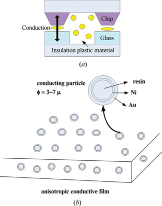
In the present TFT-LCD (Thin Film Transistor Liquid Crystal Display) panel process, IC (Integrated Circuit) flip chip packaging technology combined with anisotropic conductive film is mainly used. The function of anisotropic conductive film (ACF) is to provide the conductance of two joiners vertically, while there is an insulation effect in the horizontal direction. The anisotropic conductive film is mainly composed of conducting particles and binder. The driving IC, tape-carrier packages IC are fixed on the liquid crystal display panel (Lin et al. Citation2009; Maeda et al. Citation1999). Anisotropic conductive film is adhered to the terminals of the tape-carrier packages IC and PCB (Printed Circuit Board). The conducting particles of the anisotropic conductive film are fractured and deformed by controlling the temperature and the press fitting of pressure to form the conduction circuit. Anisotropic conductive film is mainly composed of conducting particles and insulation rubber. It also has conduction, insulation, and adherence functions. When it is heat sealed, the conductance of conducting particles is formed in the vertical direction of the thickness of film, but a monodisperse distribution is among the conducting particles. Since there is still sufficient space, the film direction is insulation, as shown in Figure a. The distribution diagram of conducting particles inside the anisotropic conductive film and its structural diagram are shown in Figure b.
Figure 1 (a) Distribution diagram of conducting particles inside sealing ACF. (b) Diagram of the structure of conducting particles inside the ACF and particle distribution inside the film (color figure available online).
The conduction method of anisotropic conductive film utilizes the indium tin oxide pole of conducting particles on a patch panel and pad of the IC for conducting electric apparatuses.
The indium tin oxide pole used in liquid crystal display is a kind of transparent conductive film coated on the surface of glass substrate by vaporization. It has good conductivity, and is called indium tin oxide glass. The conduction characteristics are the most important requirements of the Chip On Glass product process. Besides the resistance value of indium tin oxide glass, the conductivity of the integrated system should be considered. The amount of deformation and quantity of conducting particles are very important, and are closely related to the setting of each parameter in the process(Lin et al. Citation2003). Higher process pressure often leads to a larger deformation of the conducting particles, namely, the particles would flatten. Thus, the contact area of the conduction part would be enlarged, and the contact resistance decreases. Contrarily, if the pressure is too low, the contact area would be insufficient, and the contact resistance would too high, resulting in poor conduction. Therefore, it is very important to evaluate the deformation conditions of the surface of anisotropic conductive film in the optomechatronics process.
Hsieh (Citation2010) used an integrated procedure incorporating the data mining techniques to achieve the construction of yield loss model in the analysis of manufacturing process of liquid crystal display products. Chiang and Hsieh (Citation2009) used the correlation operation between quality characteristics and applied the principal component analysis to eliminate the multiple co-linearity in the inspection of LCD color filter manufacturing. Two quality characteristics and four control factors with three levels were selected to optimize the thin-film sputtering process with the entropy measurement method. (Lin et al. Citation2007; Lim and Jeong Citation2007).
However, these approaches are not suitable for the automatic inspection of fracture characteristics of anisotropic conductive film. Because the test pattern of anisotropic conductive film is very complicated. The quantity, fracture state, and distribution state of sealed conducting particles would affect the conduction between the liquid crystal display panel and its ambient control circuit. It's difficult for analysis. In this article we proposed a thinning and pattern template matching method for the automatic optical inspection system in LCD and anisotropic conductive film assembly process to improve the conventional imaging technology. This study also carried out research and development designs for inspection technology with specific image processing method in relation to the test pattern of anisotropic conductive film conducting particles. In this system, it can track, position, and inspect images of conducting particles, and measure the fracture and deformation status by using the machine vision method.
2. TEMPLATE FOR SYNCHRONOUS MULTIPLE-COMPARISON
The diagrams of conducting particles inside the panel circuit are usually complicated, and there are many irregular segments and dots. Therefore, to increase the contrast between the background and target image, the image pretreatment for the diagram to be inspected is computed (Guerra and Villalobos Citation2001; Zheng et al. Citation2002; Lin et al. Citation2008).
The image pretreatment chiefly uses the calculation of image gradient operators to reduce the noise (Salembier et al. Citation1996; Lin Citation2007).
The gradient of image f(x,y) at position (x,y) is defined as vector ∇f:
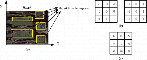
Figure 2 (a) The ACF image and the coordinate systems. (b) Prewitt mask operator. (c) 3 × 3 regional image (color figure available online).
The maximum direction of the numerical value increase of image f(x,y) direction is the gradient direction, and this increased direction can be written as α(x, y):
Another important physical quantity is the size of this vector, which is indicated as |∇f|, among which,
The gradient calculation used in this study is the improved Prewitt operators. The basic Prewitt mask utilizes two 3 × 3 masks, as shown in Figure b, to be applied in the image with a convolution operation (Kindi and Shirinzadeh Citation2007).
Taking a 3 × 3 regional image as an example, as shown in Figure c, z 1 ∼ z 9 are the gray-scale value of the pixel.
Then, the functional operation of the Prewitt mask can be written as:
Among which, g x is the new gray-scale value which corresponds the original pixel z5 to be differentiated in the horizontal direction through the Prewitt mask operation; gy is the new gray-scale value which corresponds the original pixel z5 to be differentiated vertically through the Prewitt mask operation.
While this study used the improved Prewitt mask operation, and was carried out with cross arithmetic processing of image for four kinds of 3 × 3 Prewitt mask, the operational formula can be displayed as follows:
After the operation, the final new pattern is taken to determine the fracture state of the particles. The image addition operation is f′(x,y) = f 1(x,y) + f 2(x,y); f′(x,y) is the new gray-scale value after the addition, f 1(x,y) and f 2(x,y) are the gray-scale value (Zhoua and Omarb Citation2009) of two images' corresponding pixel.
The image of conducting particles is processed by binarization before skeletonization, but the selection of its threshold affects the result of binarization treatment (Bilodeau and Bergevin Citation2005; Lin Citation1997).
Threshold k of two-value division divides all pixels of the whole image into two parts: C 0 and C 1, the variances of two aggregations are the following:
The probability density function is P i , thus, the probability density of pixel's gray-scale value to be is i. The physical significance of the probability density summation ω0 and ω1 is the area of this aggregation in the histogram. μ0 and μ1 are the distance from the centroid of area of these aggregations such as C 0 and C 1 in the histogram to the ordinate axis. σW, σB, and σ τ are within-class variance, between-class variance and total variance.
They are also the second moment of centroid of area of these aggregations and the ordinate axis. To find the optimal threshold k* of the discriminant criterion measurement is used in analysis to discuss and define the parameters:
Namely,
So, the optimal threshold of binary image can be obtained from the probability distribution. When the image is divided based on the optimized threshold k*, the second moment of the distance from the centroid of area of two aggregations, C 0 and C 1 to the centroid of area of original overall aggregation will be the maximum value.
For the image after binarization, the thinning processing method (Castleman Citation1998; Lim Citation1996) is like peeling an onion. Taking a 3 × 3 mask as an example, when it is on a 3 × 3 sub-image pixel; z 5 is the center; the quantity of nonzero pixels in eight adjacent pixels is marked as N (z 5).
For example, when z 1 = 0, z 2 = 0, z 3 = 1, z 3 = 1, z 4 = 1, z 6 = 1, z 7 = 1, z 8 = 0 and z 9 = 1, then N(z 5) = 5. Among which, if the pixel gray-scale value equals 0, in which the pixel is black; the pixel gray scale value equals 1, which means this pixel is white. For the eight adjacent pixels of z 5, taking z 1 as the start point, after returning to z 1 along the clockwise direction, and calculating the times the pixel gray scale value changes from 0 to 1, it is marked as T(z 5).
However, when N(z 5) = 0 or 1, it means all the eight adjacent pixels of pixel z 5 are white pixels, or only one pixel is a black pixel; so z 5 may be an isolated point or the furthest peripheral terminal point. z 5 will not be removed whether it is an isolated point or a terminal, namely when N(z 5) = 1, z 5 does not need to be changed to 0. When N(z 5) = 0, there should no further processing. In other words, when 2 ≦ N(z 5) ≦ 6 and z 5 = 1, z 5 needs further processing to determine whether z 5 needs to be changed to 0.
Assuming 2 ≦ N(z5) ≦ 6 is validated, if T(z 5) = 1 is also valid, when z 5 = 1, z 5 is likely to be changed to 0; to avoid the sinking of object thinning due to Z 5 being changed to 0, two more conditions z 2 · z 6 · z 8 = 0 and z 2.z 4. z 6 = 0 are made, so the sinking towards north and east when the black pixel z 5 is removed can be prevented. Based on the above, determining whether z 5 should be changed to a black pixel with gray-scale value of 0 is based on the four equations as shown in the following:
Then, when the above four equations are validated simultaneously, and z 5 = 1, z 5 will be changed to 0.
However, when thinning objects, the symmetry of thinning still needs to be considered. (C) and (D) of Equation (Equation20) tend to thinning processing in the southeast. So, to balance the thinned skeleton, this study carried out west and north thinning alternately, and the four differential equations are as follows:
When carrying out practical objects thinning, this study started the thinning processing at the furthest periphery of the object, and then carried out thinning in the other two directions according to Equation (Equation21). It alternated the two equations for computation, and carried out continuous thinning operation at the periphery of the object, until the skeleton of the object has 1 pixel width left to complete the skeletonization.
3. EXPERIMENTAL RESULTS
Figure shows the relations of conducting particle shape, conditions, and its deformation. The deformation degree and conducting conditions can be evaluated by the particle shape. As shown in Figure a, it is an anisotropic conductive film inspection image with only the protruding shapes of the conducting particles. All conducting particles are distributed in the hexagonal bump block. Therefore, when selecting a block template image as a target template, only one needs to be selected to define the average gray level and the outline of the target, as shown in Figure b. After the image pretreatment, the block in which all conducting particles are distributed, can be obtained, as shown in Figure c. Various conducting particles can be obtained from it, as shown in Figure d.
Figure 3 Relations of conducting particle shape, conditions and its deformation (color figure available online).
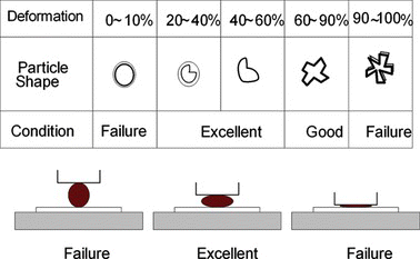
Figure 4 (a) ACF inspection image. (b) Target template. (c) Comparison result of block target template. (d) Comparison result of conducting particles (color figure available online).
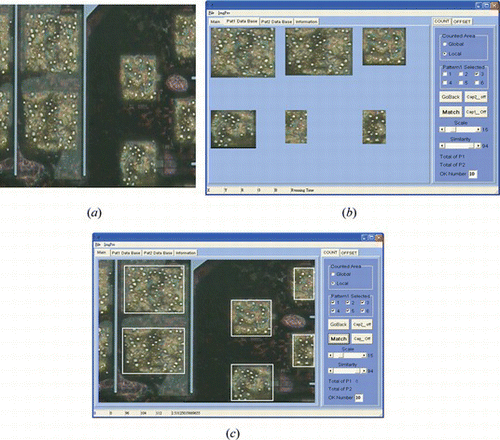
However, when the targets to be inspected are distributed in diversified block images, as shown in Figure a, the block templates need to be increased, as shown in Figure b, to carry out synchronous multiple comparison and identification for the image to be inspected. The comparison results are shown in Figure c. As shown, the diversified bump blocks in which all conducting particles are distributed are discriminated.
Figure 5 (a) ACF inspection image of the conducting particles distributed in diversified blocks. (b) Settings for complex template. (c) Result display of synchronous comparison of complex template (color figure available online).
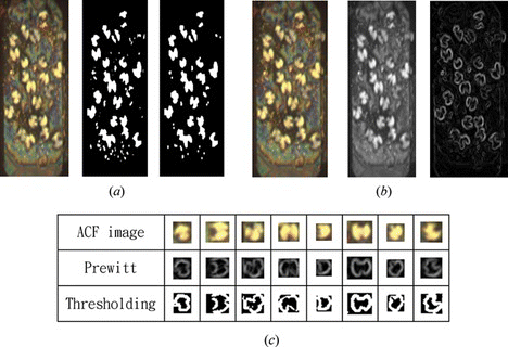
On anisotropic conductive film image pretreatment, there is a problem in image quality and noise distribution, so gray scale, close operation, binarization, improved Prewitt mask, and local scope limitation are used for alternate processing, to increase the contrast between the conducting particle image and the background. In the Figure a pretreatment series (1), the pretreatment process, from left to right, is, original image, binarization with discriminant criterion, and close operation. The primary conducting particle image is separated from the background after the processing, binarization image is formed, and the local range restriction is utilized for filtering the rest of the noise, so a preliminary analysis and judgment of conducting particle image can be completed. The pretreatment series (2) is shown as Figure b. The pretreatment process, from left to right, is the original image, gray scale and the improved Prewitt mask operation. This is the necessary procedure before skeletonizing the conducting particle image. Figure c is the binarization image obtained after each conducting particle image with the improved Prewitt mask and the binarization of discriminant criterion.
Figure 6 (a) Image pretreatment series (1). (b) Image pretreatment series (2). (c) Pretreatment of conducting particle image (color figure available online).
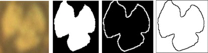
When a binarization image of a conducting particle image is obtained after the pretreatment process, the skeletonization processing is carried out, as shown in Figure . The treatment scheme, from left to right, is, original conducting particle image, binarization, improved Prewitt mask operation, and skeletonization processing.
Figure 7 Skeletonization treatment scheme (color figure available online).
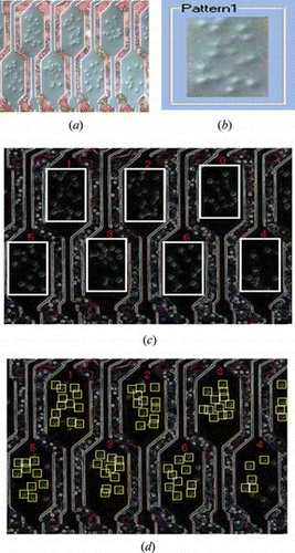
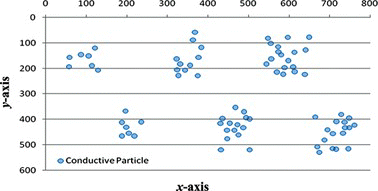
However, when the system analyzes the fracture characteristics of conducting particles of anisotropic conductive film image, it sets the bump block template image at first, as shown in Figure a, and sets the selection of conducting particle image template, as shown in Figure b. Finally, it executes the result of the comparison operation, as shown in Figure c. As shown, all bump blocks are compared, and 0 ∼ 5 are marked, which represent the position of bump blocks from Target 0 to Target 5. The fracture edge of the conducting particles is marked by the line, and the quantity and amount information of each kind of conducting particles distributed in various targets can be obtained. Figure is the image processing result of the distribution of each conducting particle. The coordinate position of each conducting particle distributed in each target, as well as the fracture edge length, can be obtained to estimate the fracture state of the conducting particles. According to the above data, the repeatability of this system can be expected to lie within 10% error probability, which is a significant improvement. It can be verified in an automatic LCD assembly production line.
Figure 8 (a) Set Bump block template image. (b) Set selection of conducting particle image template. (c) Comparison result of fracture characteristics of ACF conducting particles (color figure available online).
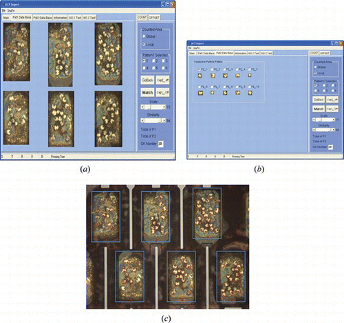
Figure 9 Result of ACF conducting particles distribution (color figure available online).
4. CONCLUSION
The primary function of the anisotropic conductive film is to provide the conductance of two joiners vertically, while there is insulation effect in the horizontal direction. It is mainly composed of conducting particles and binder, and makes the conducting particles of anisotropic conductive film fractured and deformed through the control of temperature, pressure, and joint displacement, so a conduction circuit is formed.
However, due to differences in machines, and different process conditions and conducting resin materials, various deviations are caused after press fitting, such as the quantity of conducting particles, fracture state, and the joint displacement. The deviation of the anisotropic conductive film joint position affects the conduction between the whole LCD panel and control circuit, resulting in seal OK or NG. Therefore, it is very important to develop the inspection technology for conducting particles.
Since the assembly process of liquid crystal displays is very complicated, much support of optical detection devices and image processing systems is needed to improve the quality of products and yield rate. This study utilizes the assistance of image processing technology to decrease the defection rate of products, and can be verified in an automatic production line.
ACKNOWLEDGMENTS
This work was sponsored by the Taiwan National Science Council under grant number NSC 99-2221-E-035-081.
REFERENCES
- Bilodeau , G. A. and R. Bergevin . 2005 . Matching graphs with fuzzy attributes in machine vision . International Journal of Robotics and Automation 20 ( 1 ): 206 – 277 .
- Castleman , K. R. 1998 . Digital image processing . New Jersey : Prentice Hall .
- Chiang , Y. M. and H. H. Hsieh . 2009 . The use of the Taguchi method with grey relational analysis to optimize the thin-film sputtering process with multiple quality characteristic in color filter manufacturing . Computers, Industrial Engineering 56 : 648 – 661 .
- Guerra , E. and J. R. Villalobos . 2001 . A three-dimensional automated visual inspection system for SMT assembly . Computers and Industrial Engineering 40 ( 1–2 ): 175 – 190 .
- Hsieh , K. L. 2010 . Incorporating ANNs and statistical techniques into achieving process analysis in TFT-LCD manufacturing industry . Robotics and Computer-Integrated Manufacturing 26 ( 1 ): 92 – 99 .
- Kindi , G. A. A. and B. Shirinzadeh . 2007 . An evaluation of surface roughness parameters measurement using vision-based data . International Journal of Machine Tools and Manufacture 47 ( 3–4 ): 697 – 708 .
- Lim , J. S. 1996 . Two-dimensional signal and image processing . New Jersey : Prentice Hall .
- Lim , D. C. and D. H. Jeong . 2007 . Zone-based inspection and defect classification for LCD manufacturing: trivial defect free procedure for TFT glass inspection . International Journal of Optomechatronics 1 ( 3 ): 312 – 330 .
- Lin , C. S. 1997 . Digital signal processing . Taipei : CHWA Publishing .
- Lin , C. S. , Y. L. Lay , C. C. Huan , H. C. Chang , and T. S. Hwang . 2003 . An image-based LCD positioning system utilizing the modified FHT method . Optik 114 ( 4 ): 151 – 160 .
- Lin , H. D. 2007 . Computer-aided visual inspection of surface defects in ceramic capacitor chips . Journal of Materials Processing Tech 189 ( 1–3 ): 19 – 25 .
- Lin , C. S. , C. W. Tsai , Y. C. Lu , C. Tsou , and S. C. Chang . 2007 . Automatic inspection of the width and gap of etching transistors in TFT-LCD panels using sub-pixel accuracy estimation . International Journal of Advanced Manufacturing Technology 35 : 127 – 134 .
- Lin , C. S. , Y. C. Liao , Y. L. Lay , L. C. Lee , and M. S. Yeh . 2008 . High-speed TFT LCD defect detection system with genetic algorithm . Assembly Automation 28 ( 1 ): 69 – 76 .
- Lin , C. S. , K. C. Wu , Y. L. Lay , C. C. Lin , and J. M. Lin . 2009 . An automatic temple generating method of the machine vision system in TFT LCD assembly and positioning process with genetic algorithm . Assembly Automation 29 ( 1 ): 41 – 48 .
- Maeda , S. , M. Ono , H. Kubota , and M. Nakatani . 1999 . Precise detection of short-circuit defects on TFT substrate by infrared image matching . Systems and Computers in Japan 30 ( 12 ): 72 – 84 .
- Salembier , P. , P. Brigger , J. R. Casas , and M. Pardas . 1996 . Morphological operators for image and video compression . IEEE Transaction on Image Processing 5 ( 6 ): 881 – 898 .
- Zhoua , Y. and M. Omarb . 2009 . Pixel-Level fusion for infrared and visible acquisitions . International Journal of Optomechatronics 3 ( 1 ): 41 – 53 .
- Zheng , H. , L. X. Kong , and S. Nahavandi . 2002 . Automatic inspection of metallic surface defects using genetic algorithms . Journal of Materials Processing Technology 125–126 : 427 – 433 .