
Abstract
The Tilted-Wave-Interferometer (TWI) is a non-null, full-field interferometric measuring technique for aspheric and free-form surfaces with a new degree of flexibility. The interferometer uses a set of tilted wavefronts to locally compensate the deviation of the surface under test from its spherical form. Since it is a non-null technique, there is no need for costly compensation optics. The measurement data acquisition is highly parallelized, leading to a short measurement time in the region of few seconds, by simultaneously achieving a high lateral resolution. The unique combination of these characteristics makes the TWI a perfect candidate for the integration into the process chain of aspheric and free-form surface manufacturing.
NOMENCLATURE
| CGH | = |
Computer Generated Hologram |
| IBF | = |
Ion Beam Figuring |
| I,j,k,l | = |
Index of polynomial order |
| MRF | = |
Magneto Rheological Finishing |
| M,N | = |
Normalized coordinate on Point source array |
| m,n | = |
Normalized coordinate on camera |
| OPLp | = |
Optical Path Length (P-Black Box) |
| OPLq | = |
Optical Path Length (Q-Black Box) |
| qij(M,N)/fij(X,Y) pkl(m,n) gkl(x,y) | = |
Set of orthonormal polynomials |
| S,F | = |
Spatial/Field polynomial order (Q-Black-Box) |
| s,f | = |
Spatial/Field polynomial order (P-Black-Box) |
| SUT | = |
Surface Under Test |
| TWI | = |
Tilted Wave Interferometer |
| X,Y | = |
Normalized coordinate on reference surface Eq |
| x,y | = |
Normalized coordinate on reference surface Ep |
1. INTRODUCTION
Aspheric surfaces are widely used in modern optical systems, reaching from low-cost polymer lenses in smartphone cameras to high end applications like astronomic mirrors or lithography lenses for the semiconductor fabrication.[ Citation 1 , Citation 2 ] The advantage of aspheric, compared to classical spherical elements, is the improved ability for aberration correction, due to the increased degree of freedom for the optics design. This leads to more compact and lightweight optical systems with improved optical performance at the same time. By breaking the rotational symmetry of an aspheric element a so called free-form surface is obtained. Such elements can be used to design even more sophisticated optical systems, for example systems with a folded optical path, where the elements are no longer arranged along a straight line. This additional degree of freedom can be used to obtain even more compact optical systems. Another advantage of such off-axis systems is the possibility to avoid central reflections, which is especially important for applications with coherent light sources. For some wavelengths there are no refractive materials with tolerable absorption available. Here the construction of mirror optics is the solution of choice. To avoid central obscurations, again off-axis, free-form mirrors are the solution of choice. This is for example the case in the EUV range, which will be used for the next generation of semiconductor lithography. The technology for the manufacturing of aspheric but also free-form elements has made a major progress in the last years. Technologies like ion beam figuring (IBF) and magneto rheological finishing (MRF) allow the polishing of such surfaces with high accuracy. With fast- and slow-tool-servos the application of diamond turning is expanded to non-rotationally symmetric free-forms. Most of these modern fabrication techniques are computer controlled, and therefore to fabricate a different surface geometry only the design data has to be changed to obtain the desired surface geometry. However, since the finishing of the surface is an iterative process, measurement data is needed for the control of the process. With state of the art metrology, this is often the bottleneck of the fabrication chain. Existing null-test methods that use computer generated holograms (CGH) as compensation optics have a short measurement time. However, the setup-time for the CGH, as well as the time for the alignment of the surface under test (SUT) is high. Further, since for every new design shape, a matching compensation element has to be fabricated, the technology is limited to high-volume fabrication or high end optics only. Other methods, for example stitching approaches like the scanning Fizeau interferometer[ Citation 3 ] or stitching interferometry[ Citation 4 , Citation 5 ] are more flexible, however here the measurement time is very high since the SUT has to be moved to many positions during the measurement and the data is acquired sequentially. The same disadvantages are present for tactile or optical, point wise measuring techniques. This means that with state of the art technologies the manufacturing of aspheres and free-form surfaces is metrology limited. The Tilde-Wave-Interferometer[ Citation6-8 ] which was developed at the Institute of Applied Optics (ITO) at the University of Stuttgart is a non-null, full-field measurement device for the testing of aspheric, but also free-form surfaces that do not have to show any symmetry at all. It uses a set of tilted wave-fronts to locally compensate the deviation of the surface from its spherical form. With the present setup surfaces with a deviation of up to 10° from the best-fit sphere can be measured. This is not a principal limitation, but results from the current setup. The tilted wavefronts are applied to the surface simultaneously, leading to a highly parallelized data acquisition. As a result the measurement time stays far below one minute. Like all full-field measurement techniques it has a high lateral resolution. Furthermore, neither the SUT has to be moved during the measurement, nor the orientation of the interferometer has to be changed. The combination of these unique characteristics makes the Tilted-Wave-Interferometer a perfect candidate for the integration into the process chain of asphere and free-form fabrication.
2. SETUP
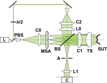
In Figure the basic setup of the Tilted-Wave-Interferometer is shown. A coherent laser source L is divided into test and a reference wave by a polarizing beam splitter PBS. The light in the test wave is used to illuminate a micro lens array that is followed by a pinhole array. These two parts serve as an array of point sources for the test wavefronts. The spherical wavefront from each point source is, after passing the beam splitter BS, collimated by C1 resulting in a set of plane wavefronts with different amounts of tilt. The tilted wavefronts are transformed to spherical wavefronts by the transmission sphere TS to compensate the basic spherical form of the SUT. In the case of surfaces with a best fit sphere of infinite radius no transmission sphere is needed. After being reflected by the SUT the wavefronts propagate back to the beam splitter, where they are reflected to the camera arm of the interferometer. In the Fourier plane an aperture stop is located, to block all light that would generate fringes with a density that violates the Nyquist criterion. After the aperture the light passes an imaging optics L1 and interferes with the reference wavefront on the camera C. The distance between the sources in the array is chosen to cover the whole SUT without gaps and a slight overlap. To avoid interference between neighboring sources the measurement is divided into four steps, with only every fourth source enabled in each step. The switching between the sources is realized by a simple aperture array that is moved in front of the micro lenses and blocks every second source in each row and column. The main difference of this approach to the scanning type interferometers mentioned above is that the acquisition of the data is highly parallelized, since all test wavefronts are applied to the surface in only four steps. Further, the SUT does not have to be moved during the measurement process. Both these advantages lead to a very short measurement time of far under a minute.
Figure 1 Schematic setup of the Tilted-Wave-Interferometer.
3. CALIBRATION
Like with every non-null test interferometer, calibration is an important task. In a null-test case the rays hit the SUT perpendicularly, and therefore the optical paths through the interferometer to the SUT and the way back are the same. Here the calibration has to cover the optical path difference (OPD) that emerges from the interferometer itself for each pixel, but independently from the SUT. Therefore it is sufficient to have a two-dimensional correction term that is subtracted from the measurement to cover the interferometer aberrations. In a non-null setup the calibration is no longer that trivial.[ Citation 9 ] Here the rays take paths through the interferometer that deviate from the null-test paths, introducing additional retrace errors to the measurement. To deal with these retrace errors a more sophisticated calibration method is required. The calibration has not only to cover the OPDs at each pixel (position on aperture) but also the field dependency of the OPDs. As a result the correction term is no longer two-dimensional but four-dimensional. In case of the Tilted-Wave-Interferometer the calibration is separated into two parts. The first part OP L q describes the illumination of the system. It contains the optical paths from the point sources of the micro lens array to a reference plane in the test area. The second part OP L p describes the imaging arm of the device, containing the optical paths from a second reference plane in the test area to the camera. In the mathematical model both parts are realized as black-box-models, which are defined as following. For the illumination part the optical path length OPL is calculated by
4. MEASUREMENT
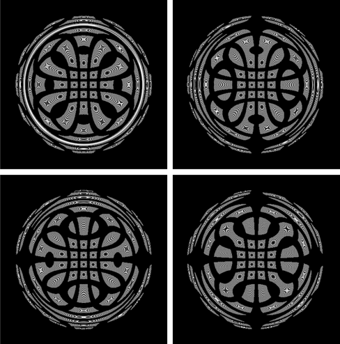
For a measurement the aspheric or free-from surface is positioned in front of the transmission sphere, in the null test position of its best-fitting sphere. The raw data for the measurement is acquired by phase shifting interferometry. To avoid interference between neighboring sources, only every second source in each row and column is turned on simultaneously, resulting in four phase measurements of the surface with different patches illuminated. In Figure the four phase maps when measuring an aspheric surface are shown. The phase maps have been calculated from the nominal black-box model of the interferometer and the nominal shape of an example asphere. The surface reconstruction is divided into two steps. In the first step the basic low frequency form of the surface is calculated. For the reconstruction of the surface under test we define a set of test rays which are distributed over the surface and the OPL of each test ray is extracted from the measurements. With the design data of the surface and the model of the interferometer that was determined in the calibration process the OPLs of the test rays can be calculated in a simulation. By a perturbation method of the polynomial surface representation and an optimization process—where this time the interferometer model is known and the surface is the unknown—the basic surface shape as well as the misalignment of the SUT during the measurement can be calculated. Since the polynomial presentation of the surface is of finite order, it only covers the basic form of the surface, but not the higher frequency errors that might also be present in the surface. For the reconstruction of these errors a second evaluation step is added. First the OPL for each pixel of the camera is calculated, using the calibrated model of the interferometer as well as the calculated polynomial surface representation and misalignment. The information about the higher frequency error is calculated by subtracting the calculated from the measured phase maps.[ Citation 11 ] With the interferometer as well as the basic form of the SUT known, not only the OPL, but also the exact path of each ray through the system can be calculated. Therefore the OPD between the measurement and the calculation at each pixel can be projected to the SUT. As a result a complete full field measurement of the asphere or free-form including not only the basic form, but also the higher frequency errors is obtained.
Figure 2 Modulo 2π phase maps calculated from the black-box model and the nominal asphere shape, with aperture array in positions 1–4 as obtained in a measurement of the TWI. (The wavelength for the calculation of the phase maps was increased for better visualization by a factor of 10).
5. ALIGNMENT
As in every interferometric measurement the alignment of the SUT is an important task. If the surface is misaligned, additional retrace errors are introduced to the measurement. When measuring spherical elements it is possible to subtract first order aberrations like tilt, defokus, and coma from the measurement since these aberrations are very likely to be artefacts from the misalignment. For aspheres or even free-form surfaces this is no longer possible. To keep the misalignment introduced uncertainties small an iterative algorithm has been developed that is capable of positioning the SUT to the test position. In case of aspheric surfaces it could be shown, that the repeatability of the position is better than 1 µm in space.[ Citation 12 ] In addition, since all the aberrations of the system, and therefore all retrace errors are known, it is possible to measure a misaligned surface without the need to position it with interferometric accuracy. The result of such a measurement is a rotated or translated point cloud, but without any additional artefacts from the misalignment. Therefore it is possible to measure the misaligned surface and correct the misalignment virtually in the evaluation algorithms.[ Citation 13 ] In simulations we could show that even if the surface is misaligned up to 10 µm in space, the error introduced through the misalignment stays below 5 nm.
6. RESULTS
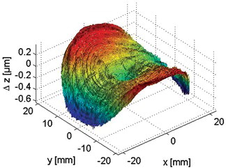
In Figure the measurement result of an aspheric surface is shown. The measurement was performed on a prototype of the TWI at the company Mahr GmbH. The surface has a deviation of the spherical form of about 600 µm and a slop deviation of about ±8°. As a comparison to the Tilted-Wave-Interferometer a measurement on a tactile UA3P Panasonic coordinate measuring machine was carried out. The surface was polished using MRF technology and the footprints of the MRF finishing are clearly visible on both measurements. In Figure a TWI measurement result of a free-form surface is shown. The surface has a strong astigmatism of about 1 mm and was fabricated using diamond turning. The grooves from the turning process can be clearly seen in the measurement. As could be shown in simulations, the measurement uncertainty is better than λ/5 peak to valley for the current setup.
Figure 3 Measurement of aspheric surface obtained by TWI (left) and comparison measurement obtained by UA3P CMM (right).
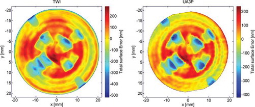
Figure 4 Measurement of diamond turned free-form surface with diamond turning marks clearly visible in the measurement.
7. CONCLUSION
The Tilted-Wave-Interferometer is a non-null test interferometer for the measurement of aspheres and free-form surfaces with a deviation of up to 10° from the spherical form. Its main benefits are the short measurement time of far under one minute compared with its high lateral resolution. Further, it is highly flexible and does not need costly compensation optics and the surface does not have to be moved during the measurement. In contrast to conventional full-field interferometers the requirements to the alignment are strongly reduced and the alignment of the SUT can be automated very well. All these advantages make it a promising metrology technique for the integration into the process chain of asphere and free-form fabrication.
Notes
Color versions of one or more of the figures in the article can be found online at www.tandfonline.com/uopt.
REFERENCES
- Braunecker , B. ; Hentschel , R. ; Tiziani , H.J. Advanced Optics Using Aspherical Elements . SPIE Press Monograph PM173 : Bellingham , WA , 2008 .
- Schulz , G. Aspheric Surfaces in Progress in Optics ; Wolf , E. , Ed. Vol. XXV . North-Holland : Amsterdam , 1988 , pp. 349–415.
- Kuechel , M.F. Interferometric measurement of rotationally symmetric aspheric surfaces . Proc. SPIE 7389/. 738916, 2009 .
- Murphy , P. ; Forbes , G. ; Fleig , J. ; Dumas , P. ; Tricard , M. Stitching interferometry: A flexible solution for surface metrology . OPTPN 2003 , 14 , 38 – 43 .
- Tricard , M. Subapertur-Stitching-Interferometrie: Messtechnik für die Asphären-Präzisionsfertigung . Photonik 2008 , 6 , 38 – 41 .
- Liesener , J. Zum Einsatz räumlicher Lichtmodulatoren in der interferometrischen Wellenfrontmesstechnik. Dissertation Universität Stuttgart, 2006 .
- Liesener , J. ; Garbusi , E. ; Pruss , C. ; Osten , W. Verfahren und Messvorrichtung zur Vermessung einer optisch glatten Oberfläche. German Patent 10 2006 057 606.3, 2006 .
- Garbusi , E. ; Pruss , C. ; Osten , W. Interferometer for precise; and flexible asphere testing . Opt. Lett. 2008 , 33 , 2973 – 2975 .
- Lowman , A.E. ; Greivenkamp , J.E. Interferometer errors due to the presence of fringes . Appl. Opt. 1996 , 35 , 6826 – 6828 .
- Garbusi , E. ; Osten , W. Perturbation methods in optics: Application to the interferometric measurement of surfaces . J. Opt. Soc. Am. 2009 , 26 , 2538 – 2549 .
- Baer , G. ; Schindler , J. ; Siepmann , J. ; Pruß , C. ; Osten , W. ; Schulz , M. Measurement of aspheres and free-form surfaces in a non-null test interferometer: Reconstruction of high-frequency errors. Proc. SPIE 8788 , 10.1117/12.2021518.
- Baer , G. ; Garbusi , E. ; Lyda , W. ; Osten , W. Automated surface positioning for a non-null test interferometer . Opt. Eng. 2010 , 49 , 095602 .
- Baer , G. ; Schindler , J. ; Pruss , C. ; Osten , W. Correction of misalignment introduced aberration in non-null test measurements of free-form surfaces . JEOS 2013 , 8 , 13074 .
- Color versions of one or more of the figures in the article can be found online at www.tandfonline.com/uopt.