
 ?Mathematical formulae have been encoded as MathML and are displayed in this HTML version using MathJax in order to improve their display. Uncheck the box to turn MathJax off. This feature requires Javascript. Click on a formula to zoom.
Abstract
We propose a novel acousto-optic (AO) devise using suspended fishbone nanobeams based on phononic and photonic potential well (PnPW and PtPW). We aim to reduce the traditional device size and eliminate the need for mirror regions in 1-D nanobeam cavity. By manipulating the frequencies of slow sound (SS) and slow light (SL) modes through geometric parameters, we can create potential wells for phonons and photons. The potential wells concentrate the waves inside the resonant cavity simultaneously, leading to an increase in AO coupling rate. We demonstrate the capability of potential wells in improving the AO coupling rate and investigate the impact of both wells. Some distribution of the phonons may affect the photons with a negative contribution, leading to a decrease in the coupling rate. Careful selection of appropriate acoustic and optical modes can overcome this limitation, making this structure a promising candidate for designing AO devices in silicon photonics.
1. Introduction
In modern society, various microelectromechanical computing components, composed of integrated circuits, have become an essential part of our daily lives. Nanoscale electronic sensors, filters, and resonators are integrated into chips for practical usage. As the demand for improved computational performance and component miniaturization grows, alternative methods, such as light circuits, are being explored to replace integrated circuits. Over the past decade, quantum computers have propelled such research further, and using light as a replacement for electricity in signal transmission has emerged as an effective approach.[Citation1–3] In the commonly employed near-infrared communication band, Si has emerged as an excellent optical waveguide material, owing to its extremely low absorption.[Citation4–6] Thanks to mature semiconductor processing technology, Si can be easily processed into components and integrated onto SiO2 substrates. Furthermore, the substantial refractive index contrast between Si (n = 3.46) and the surrounding air or SiO2 substrate (n = 1.46) makes it the preferred optical waveguide material.[Citation4–6]
In the field of designing integrated light circuits employing silicon photonics, the demand for a variety of circuit elements is also evident in optical circuits. For instance, while electrons can be stored in capacitors, photons can only prolong their lifetime through resonant cavities[Citation7–11] or decrease the speed of light in structures utilizing metamaterials.[Citation12–16] In contrast to electrons that transmit signals in conventional circuits, photons that transmit signals in optical circuits require bandwidth reduction and polarization manipulation through filters.[Citation17–21] Switching components, accomplished via transistors in computational circuits, can also be achieved in integrated light circuits using external electrical, thermal, or acoustic signals.[Citation22–25] A commonly used approach when designing light circuit components is controlling light waves using sound waves. By inputting elastic waves, conditions of light wave propagation in acousto-optic (AO) devices can be rapidly and effectively altered by inducing deformation and internal strain in the structure, thereby achieving swift control.[Citation26–31] Optomechanical devices can also convert optical signals into mechanical signals for output when reading optical signals, providing a more versatile way of reading signals in light circuits.[Citation32,Citation33]
As early as 2009, Matt et al. proposed a one-dimensional optomechanical crystal that could be integrated into a planar lightwave circuit.[Citation26] They designed a 1-D photonic crystal by creating periodic rectangular holes in a long and narrow silicon waveguide, forming a resonant cavity by changing the lattice constant in the central region and fixing the lattice constant in the mirror region on the outside to form reflective area. Through experiments, they confirmed that photons at 200 THz and phonons at 2 GHz can be coupled in the structure. Since then, 1-D optomechanical waveguides have been extensively studied. Initially, most of the research used similar hole-digging methods to design optomechanical waveguides. However, they were limited by the difficulty of generating phonon band gaps for mirror regions. In 2011, Pennec et al. began adding wing-shaped structures extending outward to the outside of the hole-dug silicon photonic waveguide to make it easier to generate phonon band gaps in the optomechanical crystal.[Citation27] In 2012, Hsiao et al. changed the position of air holes originally in the center of the waveguide to two semicircles on both sides of the waveguide, thus designing a fishbone-shaped phoxonic crystal.[Citation28] This design greatly enhanced the AO coupling by using photons and phonons with slow group velocities generated in the structure. In 2017, Chiu et al. designed a defect with a gradually varying period constant in the fishbone-shaped structure, forming a high-efficiency AO coupling resonant cavity and analyzed the relationship between acoustic modes and AO coupling rate.[Citation29] Most recently, in 2022, Daniel et al. integrated the structure of surface acoustic waves and designed an on-chip electro-opto-mechanical system at room temperature. In the experiment, the microwave signal was successfully converted to an optical wave signal with high sensitivity.[Citation31]
In these studies, the mirror regions that possess both photonic and phononic bandgaps play a crucial role in each structure. The number of periods in the mirror region should be at least five or more to effectively utilize the bandgap and form a reflective area on both sides of the cavity. To ensure smooth entry of photons and phonons into the cavity region through the mirror region and to reduce losses, the geometric parameters of the structure should be gradually changed over several periods. Therefore, most acousto-optic structures require a length of about 10 µm. This study aims to provide an alternative approach to designing the resonant cavity and overcoming the limitations of using mirror regions. The structure will utilize slow light (SL) and slow sound (SS) modes to enhance the AO coupling efficiency and phononic potential wells (PnPW) and photonic potential wells (PtPW) to confine photons and phonons within the resonant cavity.
In traditional quantum wells, electrons are confined to specific regions by exploiting the discrete energy levels available in the material. The energy of both electrons and photons can be calculated using the Planck-Einstein relationship, E = hν, with their energy levels represented by frequency. Similarly, phonons can be distinguished by frequency to indicate their relative energy levels.[Citation34] In our previous study, a 1-D waveguide with a PnPW that employs phonons with different frequencies was designed.[Citation35] When the frequency of the acoustic mode in the unit cell changes due to geometric parameters, it can be treated as having corresponding phonon energy levels, similar to the electron energy level in dielectric materials. By properly combining multiple unit cells with different geometric parameters, PnPW can be established using the phonon energy levels in each unit of the structure. Using a similar approach, PtPW can also be designed in the cavity by combining the photon energy levels in the structure.
In this study, we aim to design a phoxonic crystal waveguide device that replaces the traditional mirror region with PnPW and PtPW simultaneously, leading to the reduction in the size of the component. The paper’s structure is organized as follows: Section 1 introduces the unit cell, geometric parameters of the fishbone structure, as well as the SL and SS modes used in this study. In Section 2, we describe the quantification of the AO coupling rate g value used in the AO devices, which is determined by the frequency shift of the SL mode due to the moving boundary (MB) effect and the photo-elastic (PE) effect. Section 3 discusses the impact of PnPW on the g value in the structure without PtPW. In Section 4, we introduce the design with PtPW and further analyze its effect on the g value. Finally, we summarize the conclusions of this study.
2. Structure units and mode analysis
We utilized a 1-D nanobeam in a fishbone shape as the carrier for SS and SL transmission. By periodically excavating air holes on both sides of a silicon nanobeam and elongating the regions between the holes into wing-like structures, the fishbone shape was formed. displays the top view (top) and side view (bottom) of the unit cell in a periodic fishbone structure, and labels the corresponding geometric parameters. To control the wavelength of the optical wave mode to be near 1,550 nm, the lattice constant a was set to 440 nm, and the radius of the excavated air holes r was set to 0.32a to achieve the acoustic wave mode close to the optical wavelength. Additionally, the thickness of the nanobeam H was set to 220 nm, and the base width of the nanobeam w was set to 440 nm.
Figure 1. (a) The top view and side view of the fishbone unit cell with geometric parameters. The (b) phononic band structure and (c) photonic band structure are shown by blue circles with the SS mode and SL mode indicated by red circles and red arrow respectively in the corresponding figure. (d) The displacement field distribution of the SS mode and (e) the electric field in x-component of the SL mode are depicted below the band structures.
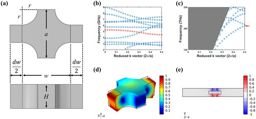
In order to facilitate the modulation of the wave modes of light and sound, we have further defined the length of the fishbone wing, dw, and the lattice constant, a′, as illustrated in . Both parameters are adjusted based on the basic width, w, and the basic lattice constant, a. respectively depict the phononic and photonic band structures of the structure with a′= a and dw = 0.5w, with the operating SS mode and SL mode marked in red. By applying periodic boundary conditions on the upper and lower surfaces of the unit cell in the z-direction depicted in the top view of , we can use the finite element method (FEM) to calculate the eigenmodes of the structure under different k-vector conditions and obtain the energy band structure.
Based on the definitions of the horizontal and vertical axes in the band structure, the group velocity of each mode can be calculated using the first derivative at each point. In , the SS mode is marked with red circles and its displacement field is represented in . Observing , it is evident that the SS mode is primarily driven by the vibration of the wings, while the central region of the nanobeam experiences almost no displacement in comparison to the wing region. Thus, the resonance frequency of the SS mode can be adjusted by changing the length of the wings, i.e., by adjusting dw. On the other hand, shows the photonic band structure of the fishbone structure, where the gray area represents the light cone. Modes located within the light cone would result in speeds exceeding the speed of light in a vacuum when calculating the first derivative, so they are not considered in this study.
The mode indicated by the red arrow is the SL mode in the structure. Although the first derivative of the mode is not close to 0 for k < 0.5, it meets the desired slow-light condition at k = 0.5. This SL mode is primarily controlled by the electric field component in the x-direction, as shown in . We can analyze it by studying the distribution of this component. displays the x component of the electric field of this mode. From the figure, we can observe that the electric field is distributed in the center of the region with holes, and the wavelength is approximately double that of a. Based on the electric field distribution, we can infer that changing the length of the wings will not affect the frequency of the light wave, and the frequency of the SL mode can be modulated by changing the lattice constant of the unit, which is a’.
To validate the capability of modulating SS and SL modes using dw and a′, we plot the variations of SS and SL modes as a function of these two parameters in . depicts the change in SS and SL modes with dw/w in a structure with a fixed a′/a ratio. To ensure that the frequency shift of modes in different structures with different a′/a ratios exhibit similar trends, we show the frequency shift of SS and SL modes in two structures with a′/a = 1 (solid line) and a′/a = 0.5 (dotted line). As seen in , the SS mode, indicated by the blue triangle, demonstrates a decrease in frequency with increasing dw in both structures, while the SL mode, indicated by the orange circle, remains almost unchanged. This indicates that adjusting dw (the length of the wings) affects only the SS mode.
Figure 2. The resonance frequency of the SS mode and the SL mode varying with (a) the wing length dw and (b) the lattice constant a’.
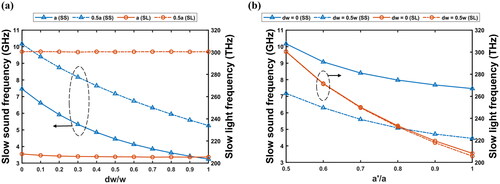
On the other hand, shows the trend of the SS and SL modes with respect to changes in a′/a in a structure with a fixed dw/w ratio. To ensure that the frequency shift of modes in structures with different dw/w ratios exhibit the same trend, the frequency shift of the SS and SL modes in structures with dw/w = 0 (solid line) and dw/w = 0.5 (dashed line) are displayed. From , it can be seen that changes in a′ impact both the acoustic and optical wave modes. As the value of a′/a decreases, the frequency of both the SS and SL modes increases, with a larger impact on the optical wave mode. The results show that the modulation method based on the electric field distribution that was mentioned in the previous paragraph is workable. As the modes in the structure are closely related to the geometric structure parameters, we kept the radius of air holes in each unit maintain a ratio of 0.32 with the lattice constant when changing the lattice constant a′. The change in the lattice constant then affects the width of the wing and thus the resonance frequency of the acoustic wave. However, the SS mode is mainly dominated by the length of the wing, and the width of the wing has a relatively minor impact on the SS mode, so adjusting a′ can still serve as a means of modulating the frequency of the SL mode.
3. Acousto-optic coupling ratio
The coupling rate g represents the performance of the structure as an AO device, with a higher value indicating a better ability of sound waves to modulate light waves. In the AO coupling element, the calculation of the g value needs to consider two effects induced by sound waves: the moving boundary (MB) effect caused by the deformation of the structure and the photo-elastic (PE) effect caused by the strain generated in the structure during deformation that changes the local refractive index. When the frequency of the light wave is ω0, the g value generated by the two effects can be calculated using the following formula and presented as a frequency shift of the light wave mode:[Citation29]
(1)
(1)
(2)
(2)
In formula (1), Q is the normalized displacement field, is the normal vector of the structure surface; E is the electric field, D is the electric displacement field, and the subscripts
and
denote the components parallel and perpendicular to the structure surface, respectively. Then take the volume integral of the inner product of the E field and D field in the AO cavity.
represents the relative permittivity difference between the structural material and the surrounding medium, which is the difference between silicon and air in this paper, and
is the reciprocal difference of relative permittivity. In formula (2),
where n is the refractive index of silicon,
is the photo-elastic tensor, and
is the strain tensor generated by sound waves. Finally,
is the zero-point momentum of the resonant structure, where
is the reduced Planck constant,
is the effective mass generated by the sound wave displacement field in the structure, and
is the frequency of the sound wave.
The total AO coupling rate of the structure can be obtained by adding the coupling rate produced by the two effects:
It can be noticed that the calculated g value can be positive or negative, representing the frequency shift of the optical mode to a higher or lower frequency. When discussing the AO coupling rate in the structure, that is, the modulation ability of sound on light, the |g| value will be taken for discussion, representing the amount of frequency shift of the optical mode.
4. Phononic potential well nanobeam
Using the relationship between resonance frequency and geometric parameters, structures with PnPW and PtPW can be designed by combining units with resonance modes in different frequencies in a fishbone nanobeam. illustrates the structure of a fishbone nanobeam cavity comprising seven gradually varying unit cells, with two half-cells located on both sides and five waveguide units connected to the half-cells, respectively. The width of each waveguide unit is w, and the length is a, which is used to set up the waveguides before and after the structure in the simulation. To simulate the suspended nanobeam, the bottom surfaces of the outermost three waveguide units on both ends are fixed boundaries representing the connection surface fixed on the substrate. During the frequency response transmission simulation, the optical signal is introduced from the left of the waveguide and passes through the structure along the nanobeam towards the right side. The acoustic signal is applied from the top surface of the fourth unit on the left, and reflection is avoided by setting the loss factor in the outermost three waveguide units on both ends.
Figure 3. (a) The full sketch of the fishbone nanobeam cavity with parameter denotations. (b) The PnPW line shape of the Type α and β structures. (c) The displacement field of the SS mode at 5.744 GHz and (d) the Ex field distribution of the SL mode calculated by the eigenvalue solver in Type α structure.
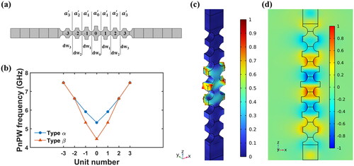
To facilitate discussion, we have assigned labels to each unit of the nanobeam. With the center unit 0 as the reference, the units on the right are sequentially numbered from 1 to 3, while those on the left are numbered from −1 to −3, as shown in . The geometric parameters of the center and right units are denoted as a′0, a′1, a′2, a′3, and dw0, dw1, dw2, dw3, respectively, based on their corresponding unit numbers. The geometric parameters of the left units are arranged in a mirror-image relationship with those on the right, as depicted in the figure.
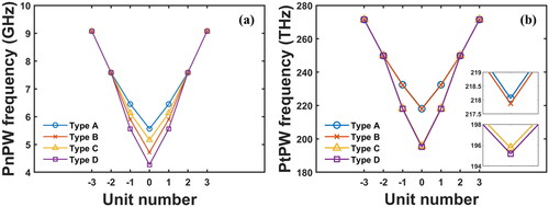
In this section, we aim to investigate the influence of PnPW by maintaining constant lattice constants in the nanobeam (a’0 = a’1 = a’2 = a’3 = a) and varying only the wing lengths of each unit. We propose two PnPW fishbone structures, denoted as Type α and Type β. In Type α, the wing lengths are dw0 = 0.3w, dw1 = 0.2w, dw2 = 0.1w, and dw3 = 0. The center unit has the longest wing length, which gradually decreases to both sides until the −3 and 3 units with a base width of w, and then passes through an additional half unit to connect with the outer waveguide unit. In the Type β structure, the wing length of the central unit increases to 0.5w, and it decreases at intervals of 0.2w until the −3 and 3 units, and then connects to the waveguide unit (dw0 = 0.5w, dw1 = 0.3w, dw2 = 0.1w, and dw3 = 0) through additional half units. presents the detailed parameters of both structures. By utilizing symmetrically varying geometric variables, we can regulate the frequency of the SS mode in each unit to exhibit the valley trend, as shown in , and form the PnPW. The PnPW of Type α and Type β structures are represented by blue circles and orange triangles, respectively, in . It is evident that the potential well of Type β has a greater depth than Type α within the same well width range. Our previous studies demonstrate that this design can enhance the Q value of the acoustic mode in the structure,[Citation35] which is expected to improve the efficiency of AO coupling.
Table 1. Geometry parameter ratio of all the six types of fishbone structures.
Through the frequency response analysis, we identified the SS mode in Type α structure at 5.744 GHz in the acoustic spectrum and the SL mode at 203.54 THz in the optical spectrum, which exhibit field distributions similar to those illustrated in , respectively. The displacement field distribution of the SS mode and the Ex field distribution of the SL mode are shown in , respectively. illustrates that the SS mode is primarily localized in the center units (−1 ∼ 1) of the fishbone structure. The displacement field reveals that the maximum displacement is observed at the end of the wings, while there is a relatively small amount of displacement at the center of the fishbone. In , the Ex field is observed to be uniformly distributed throughout the fishbone structure. By utilizing EquationEqs. (1)(1)
(1) and Equation(2)
(2)
(2) , we calculated gMB = −0.1039 MHz, gPE = −0.0057 MHz, and a total coupling rate of |g| = 0.1096 MHz for this structure. Based on the obtained g values, we found that the modulation effect produced by the MB effect is greater than the PE effect when the SS mode and the SL mode in are coupled, indicating that the structural displacement caused by the acoustic mode in exhibits better modulation ability than the refractive index change induced by the strain distribution in the structure.
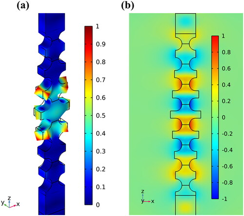
In , the SS and SL modes in the Type β fishbone are observed at the frequency of 5.137 GHz in the acoustic spectrum and the frequency of 204.3 THz in the optical spectrum, respectively. Similar to Type α, shows that the displacement field of the SS mode is concentrated within the central −1 ∼ 1 unit, while the Ex field in is evenly distributed within the fishbone structure. In the Type β structure, the values of gMB, gPE, and the total coupling efficiency |g| are −0.5774 MHz, −0.0141 MHz, and 0.5633 MHz, respectively. Numerically, it is evident that optimizing the acoustic mode with a deeper PnPW can effectively enhance the efficiency of AO coupling without optimizing the optical modes. Based on this idea, we further designed for the optimization of the optical modes.
Figure 4. (a) The displacement field of the SS mode at 5.137 GHz and (b) the Ex field distribution of the SL mode calculated by the eigenvalue solver in Type β structure.
5. AO potential well nanobeam
In order to achieve both PtPW and PnPW in the fishbone structure, we manipulated the frequency of the SL mode by adjusting the lattice constant a′ of each unit in the fishbone structure. Similar to the approach used to discuss PnPW, we created two types of PtPWs with the following sets of geometric parameters: a′0 = 0.9a, a′1 = 0.8a, a′2 = 0.7a, a′3 = 0.6a and a′0 = 1.1a, a′1 = 0.9a, a′2 = 0.7a, a′3 = 0.6a. It can be noticed that the lattice constant of the outer two unit cells are keep in 0.7a and 0.6a in these two types of design to keep the width of the PtPW. By combining these with the wing length parameters from the last section, we designed a total of four fishbone structures, denoted as Type A, Type B, Type C, and Type D, listed in . These structures can be classified into two groups based on their PnPW as Type A, C and Type B, D, and two groups based on their PtPW as Type A, B and Type C, D.
shows the PnPW and PtPW of the four structures. Since changing the lattice constant also slightly affects the SS mode, it can be observed that Type A, C and Type B, D, which have the same wing length configuration, do not have exactly the same PnPW in . It can be seen that structures with a larger lattice constant configuration, such as Type C and D, exhibit relatively deeper wells within the group with the same wing length configuration. On the contrary, the PtPW has shown in clearly presents two different depths of potential wells, confirming that the variation of wing length has little influence on the SL mode. The insets show slight differences between the PtPW in the Type A and B structures and the Type C and D structures, respectively.
Figure 5. (a) The PnPW line shape and (b) The PtPW line shape of the Type A to D structures. The inset show the tiny difference between Type A, B and Type C, D.
When deeper PnPW with the same well width have been found to effectively improve the Q value of acoustic modes in our previous studies, a similar effect is expected in PtPW structures, where higher optical quality should be induced by deepening the potential well depth and increasing the coupling rate. In , we first analyzed Type A and Type B structures with shallower PtPW. displays the displacement field of the SS mode and the Ex field of the SL mode of Type A and Type B, and their corresponding frequencies are listed in . It can be observed from that when a′ is adjusted to control the optical wave, the two PnPWs still concentrate the SS mode within the central three units. In contrast, illustrates that the PtPW concentrates the SL mode in the central unit (on both sides of the dashed line), while higher-order modes also appear in the outer units. Unlike Type α and β without designed PtPW, the spatial structure along the periodic direction of the PtPW fishbone is no longer uniform, resulting in more resonant conditions that enable higher-order modes to exist in the potential well under the corresponding resonant condition.
Figure 6. (a) The displacement field of the SS mode at 6.283 GHz and (b) the Ex field distribution of the SL mode calculated by the eigenvalue solver in Type A structure. (c) The displacement field of the SS mode at 5.717 GHz and (d) the Ex field distribution of the SL mode calculated by the eigenvalue solver in Type B structure.
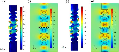
Table 2. Resonant frequencies of the SS modes and SL modes and the coupling rates of the six types fishbone structures.
Using EquationEqs. (1)(1)
(1) and Equation(2)
(2)
(2) , we can calculate the AO coupling rate of Type A and Type B. In Type A structure, gMB = −0.8789 MHz, gPE = 0.0104 MHz, and the total coupling efficiency |g| = 0.8685 MHz. In the Type B structure, the values of gMB, gPE, and the total coupling rate |g| are −0.9118 MHz, 0.0132 MHz, and 0.8986 MHz, respectively, as presented in . By comparing the two structures, we can observe that the deeper potential well of the PnPW design can still effectively increase the g value of Type B. Additionally, comparing Type A and B with Type α and β, we can infer that the incorporation of PtPW to the original PnPW design can significantly enhance the g value. However, we can also observe that the enhancement of PnPW to the g value in the Type A and B group is diluted under the influence of PtPW compared to the Type α and β group.
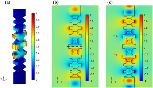
Next, we increased the depth of PtPW and designed two fishbone structures, Type C and Type D. displays the displacement field of the SS mode and the Ex field of the SL mode of the Type C structure. With the deeper potential well providing more space to accommodate modes, we obtained two modes that are concentrated in the cavity by the potential well through the frequency response solver, which are the first-order mode at 201.76 THz in and the second-order mode at 214.76 THz in . As the PtPW in the Type C and Type D structures is deeper than in the Type A and Type B structures and the ±1 units in Type C and Type D have the same a′ as the 0 units in Type A and Type B, which means the same optical resonance condition, the Ex field distribution shows that the first-order mode mainly exists on both sides of the central 0 unit (both sides of the dashed lines), and the second-order mode mainly exists on both sides of the ±1 unit, as indicated by the arrows in . By coupling the two optical modes with the acoustic modes, the respective coupling rates |g201| = 1.2086 MHz and |g214| = 1.2289 MHz are obtained, both of which show considerably high coupling rates. This result preliminarily demonstrates that increasing the depth of PtPW indeed has a positive effect on the overall g value and can significantly enhance it, leading to better optimization results.
Figure 7. (a) The displacement field of the SS mode in Type C structure at 5.772 GHz. The Ex field distribution of (b) the first-order SL mode and (c) the second-order SL mode calculated by the eigenvalue solver in Type C structure are shown. The dashed line in (b) represents the symmetry axis of the cavity, and the arrows in (c) indicate the center of the −1 and 1 unit cells.
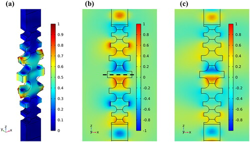
The displacement field of the SS mode and the Ex field of the SL mode for the Type D structure are presented in . As in the Type C structure, the deeper PtPW in the Type D structure results in two SL modes, located at 201.8 THz and 214.88 THz, respectively, as shown in . The first-order mode in primarily exists on both sides of the dashed line in the central 0 unit, while the second-order mode in shows an over concentrated distribution. In the C and D groups with the deeper PtPW, the Type D structure also features a deeper PnPW than Type C and is expected to have the highest coupling rate. However, the coupling rate induced by the two SL modes is only |g201| = 0.5511 MHz and |g214| = 0.6796 MHz, respectively. shows that the g value of Type D is not only lower than that of Type C but also lower than that of Type A and B, with only higher values than that of Type α and β. This may imply that there are some limitations to confining acoustic and optical waves solely by potential wells.
Figure 8. (a) The displacement field of the SS mode in Type D structure at 5.2173 GHz. The Ex field distribution of (b) the first-order SL mode and (c) the second-order SL mode calculated by the eigenvalue solver in Type D structure are shown. The dashed line in (b) represents the symmetry axis of the cavity.
To explain the abrupt reduction in g, we can observe the dominant factor gMB in EquationEq. (1)(1)
(1) that affects the coupling rate. The main factors affecting gMB are the electromagnetic (EM) energy and the displacement perpendicular to the surface. Since the displacement fields in Types A, B, C, and D are similar, we can focus on the EM energy in each structure. To visualize the energy distribution of the modes, we utilized the eigenmode solver to compute the existence form of each mode in every structure, as illustrated in . We normalized the energy of each structure by that of Type D and restricted the color bar to the range of 0 to 1. Consequently, areas with values above 1 will appear darker as the numerical values increase, enabling us to compare the structures more easily. It is evident that in Type α and β, without the PtPW, the energy is evenly distributed in the nanobeam structure, whereas in Types A, B, C, and D, the energy is more focused on unit 0.
Figure 9. The EM energy of the SL modes in all the six types of fishbone structures. The field distributions represent the corresponding structure that denoted at the left bottom corner of each figure, which are (a) Type α, (b) Type β, (c) Type A, (d) Type B, (e) Type C in 201 THz, (f) Type D in 201 THz, (g) Type C in 214 THz, and (h) Type D in 214 THz.
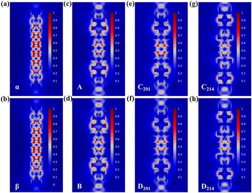
Examining the six SL modes in structures A, B, C, and D, it is apparent that the EM energy in the Type C structure is stronger than in the other structures, consistent with its highest coupling rate. Comparing the two Type C modes in and the two Type D modes in , it is also evident that the 201 THz mode has a stronger electric field energy in the central unit, indicating that the 201 THz SL mode is the ground state in the PtPW of Type C and D structures, while the 214 THz mode is the second state. Observing , it can be noted that the EM energy in Type A and B is weaker than that in Type C but greater than that in Type D, explaining why the coupling rate in the D structure is only slightly higher than that in α and β.
From another perspective, we can also analyze the displacement field. Since the electromagnetic energy is distributed in the center of the nanobeam, while the displacement field is mainly distributed at the end of the wings, it can have a significant impact on the AO coupling. Among the four structures, Type B and Type D with longer wings are more susceptible to the influence of the coupling due to the displacement field being distributed further from the center of the nanobeam. The maximum displacement values for the four structures are as follows: Type A: Type B:
Type C:
Type D:
From the numerical values, the maximum displacement caused by acoustic waves is very close. Type B, with a relatively slender wing, has the largest displacement and effectively compensates for the disadvantage of the dispersed distribution of the displacement field and EM field. Conversely, the relatively small displacement in Type D cannot provide sufficient contribution to the coupling rate, resulting in a low coupling rate.
Therefore, although both PnPW and PtPW can concentrate the corresponding sound field and light field in the resonant cavity, the distribution of the field will have a considerable impact on the coupling rate. Due to the coupling rate is not only affected by the strength and the concentrating rate of the acoustic and optical fields but also the overlap area between the fields, a too-small mode volume of one of the fields may give a negative contribution instead. In other words, though the acoustic mode and optical mode used in this study that can be manipulated respectively benefit from the separated distribution, the less overlapping area between the two fields should reduce the coupling rate. Thus, improving the coupling rate by deepening the potential well also has certain limitations, and the design of the potential well structure in the resonant cavity needs to be carefully considered.
6. Conclusion
In this study, we present a novel approach for designing AO waveguide devices using PnPW and PtPW. By adjusting the geometric parameters, PnPW and PtPW can be designed in a suspended nanobeam based on the different resonant conditions of phonons and photons. The use of PnPW and PtPW allows for the concentration of acoustic and optical waves inside the resonant cavity, eliminating the need for mirror regions and reducing device size. Our numerical calculations show that the PnPW structure has a significant impact on improving the AO coupling rate, and combining it with PtPW has the potential to further enhance the coupling rate. However, our results also reveal that when the phonons are too concentrated by the PnPW structure, it may affect the concentration of photons by the PtPW, leading to a decrease in efficiency in certain structures. Furthermore, differences in the distribution areas of phonon and photon modes can also result in decreased coupling rate. By carefully selecting appropriate acoustic and optical modes, we believe that this structure has tremendous potential for AO device design in silicon photonics.
Disclosure statement
The authors report there are no competing interests to declare.
References
- O’Brien, J.L. Optical quantum computing. Science 2007, 318, 1567–1570.
- Perez-Garcia, B.; Francis, J.; McLaren, M.; Hernandez-Aranda, R.I.; Forbes, A.; Konrad, T. Quantum computation with classical light: The Deutsch algorithm. Phys. Lett. A 2015, 379, 1675–1680. DOI: 10.1016/j.physleta.2015.04.034.
- Blais, A.; Girvin, S.M.; Oliver, W.D. Quantum information processing and quantum optics with circuit quantum electrodynamics. Nat. Phys. 2020, 16, 247–256. DOI: 10.1038/s41567-020-0806-z.
- Spitzer, W.; Fan, H.Y. Infrared absorption inn-type silicon. Phys. Rev. 1957, 108, 268–271. DOI: 10.1103/PhysRev.108.268.
- Jalali, B.; Fathpour, S. Silicon photonics. J. Lightwave Technol. 2006, 24, 4600–4615. DOI: 10.1109/JLT.2006.885782.
- Hochberg, M.; Harris, N.C.; Ding, R.; Zhang, Y.; Novack, A.; Xuan, Z.; Baehr-Jones, T. Silicon photonics: The next fabless semiconductor industry. IEEE Solid-State Circuits Mag. 2013, 5, 48–58. DOI: 10.1109/MSSC.2012.2232791.
- Preble, S.F.; Xu, Q.; Lipson, M. Changing the colour of light in a silicon resonator. Nature Photon. 2007, 1, 293–296. DOI: 10.1038/nphoton.2007.72.
- Mai, T.T.; Hsiao, F.-L.; Lee, C.; Xiang, W.; Chen, C.-C.; Choi, W.K. Optimization and comparison of photonic crystal resonators for silicon microcantilever sensors. Sens. Actuators, A 2011, 165, 16–25. DOI: 10.1016/j.sna.2010.01.006.
- Dai, D.; Bauters, J.; Bowers, J.E. Passive technologies for future large-scale photonic integrated circuits on silicon: Polarization handling, light non-reciprocity and loss reduction. Light. Sci. Appl. 2012, 1, e1-e1–e1. DOI: 10.1038/lsa.2012.1.
- Heidler, P.; Schneider, C.M.F.; Kustura, K.; Gonzalez-Ballestero, C.; Romero-Isart, O.; Kirchmair, G. Non-Markovian effects of two-level systems in a niobium coaxial resonator with a single-photon lifetime of 10 milliseconds. Phys. Rev. Applied 2021, 16, 034024. DOI: 10.1103/PhysRevApplied.16.034024.
- Ravi, J.; Chandrasekar, R. Micromechanical fabrication of resonator waveguides integrated four‐port photonic circuit from flexible organic single crystals. Adv. Opt. Mater. 2021, 9, 2100550. DOI: 10.1002/adom.202100550.
- Krauss, T.F. Slow light in photonic crystal waveguides. J. Phys. D: Appl. Phys. 2007, 40, 2666–2670. DOI: 10.1088/0022-3727/40/9/S07.
- Monat, C.; Corcoran, B.; Pudo, D.; Ebnali-Heidari, M.; Grillet, C.; Pelusi, M.D.; Moss, D.J.; Eggleton, B.J.; White, T.P.; O'Faolain, L.; Krauss, T.F. Slow light enhanced nonlinear optics in silicon photonic crystal waveguides. IEEE J. Select. Topics Quantum Electron. 2010, 16, 344–356. DOI: 10.1109/JSTQE.2009.2033019.
- Yan, S.; Zhu, X.; Frandsen, L.H.; Xiao, S.; Mortensen, N.A.; Dong, J.; Ding, Y. Slow-light-enhanced energy efficiency for graphene microheaters on silicon photonic crystal waveguides. Nat. Commun. 2017, 8, 14411. DOI: 10.1038/ncomms14411.
- Elshahat, S.; Abood, I.; Khan, K.; Yadav, A.; Wang, Q.; Liu, Q.; Lin, M.; Tao, K.; Ouyang, Z. Ultra-wideband slow light transmission with high normalized delay bandwidth product in w3 photonic crystal waveguide. Superlattices Microstruct. 2018, 121, 45–54. DOI: 10.1016/j.spmi.2018.07.025.
- Lalanne, P.; Coudert, S.; Duchateau, G.; Dilhaire, S.; Vynck, K. Structural slow waves: Parallels between photonic crystals and plasmonic waveguides. ACS Photonics 2019, 6, 4–17. DOI: 10.1021/acsphotonics.8b01337.
- Li, B.; Hsiao, F.-L.; Lee, C. Computational characterization of a photonic crystal cantilever sensor using a hexagonal dual-nanoring-based channel drop filter. IEEE Trans. Nanotechnology 2011, 10, 789–796. DOI: 10.1109/TNANO.2010.2079942.
- Zhang, J.; Zhang, H.; Chen, S.; Yu, M.; Lo, G.Q.; Kwong, D.L. A tunable polarization diversity silicon photonics filter. Opt. Express. 2011, 19, 13063–13072. DOI: 10.1364/OE.19.013063.
- Liu, Y.; Hotten, J.; Choudhary, A.; Eggleton, B.J.; Marpaung, D. All-optimized integrated RF photonic notch filter. Opt. Lett. 2017, 42, 4631–4634. DOI: 10.1364/OL.42.004631.
- Daulay, O.; Liu, G.; Ye, K.; Botter, R.; Klaver, Y.; Tan, Q.; Yu, H.; Hoekman, M.; Klein, E.; Roeloffzen, C.; Liu, Y.; Marpaung, D. Ultrahigh dynamic range and low noise figure programmable integrated microwave photonic filter. Nat. Commun. 2022, 13, 7798. DOI: 10.1038/s41467-022-35485-x.
- Liu, X.; Ren, G.; Xu, X.; Dubey, A.; Feleppa, T.; Boes, A.; Mitchell, A.; Lowery, A. ‘Dial up’ photonic integrated circuit filter. J. Lightwave Technol. 2023, 41, 1775–1783. DOI: 10.1109/JLT.2022.3226685.
- Demir, H.V.; Sabnis, V.A.; Fidaner, O.; Jun-Fei, Z.; Harris, J.S.; Miller, D.A.B. Multifunctional integrated photonic switches. IEEE J. Select. Topics Quantum Electron. 2005, 11, 86–96. DOI: 10.1109/JSTQE.2004.841715.
- Fang, Q.; Song, J.F.; Liow, T.-Y.; Cai, H.; Yu, M.B.; Lo, G.Q.; Kwong, D.-L. Ultralow power silicon photonics thermo-optic switch with suspended phase arms. IEEE Photon. Technol. Lett. 2011, 23, 525–527. DOI: 10.1109/LPT.2011.2114336.
- Kapfinger, S.; Reichert, T.; Lichtmannecker, S.; Muller, K.; Finley, J.J.; Wixforth, A.; Kaniber, M.; Krenner, H.J. Dynamic acousto-optic control of a strongly coupled photonic molecule. Nat. Commun. 2015, 6, 8540. DOI: 10.1038/ncomms9540.
- Liu, X.; Qiao, Q.; Dong, B.; Liu, W.; Xu, C.; Xu, S.; Zhou, G. MEMS enabled suspended silicon waveguide platform for long-wave infrared modulation applications. Int. J. Optomechatronics 2022, 16, 42–57. DOI: 10.1080/15599612.2022.2137608.
- Eichenfield, M.; Chan, J.; Camacho, R.M.; Vahala, K.J.; Painter, O. Optomechanical crystals. Nature 2009, 462, 78–82. DOI: 10.1038/nature08524.
- Pennec, Y.; Rouhani, B.D.; Li, C.; Escalante, J.M.; Martinez, A.; Benchabane, S.; Laude, V.; Papanikolaou, N. Band gaps and cavity modes in dual phononic and photonic strip waveguides. AIP Adv. 2011, 1, 041901. DOI: 10.1063/1.3675799.
- Hsiao, F.-L.; Hsieh, C.-Y.; Hsieh, H.-Y.; Chiu, C.-C. High-efficiency acousto-optical interaction in phoxonic nanobeam waveguide. Appl. Phys. Lett. 2012, 100, 171103. DOI: 10.1063/1.4705295.
- Chiu, C.C.; Chen, W.M.; Sung, K.W.; Hsiao, F.L. High-efficiency acousto-optic coupling in phoxonic resonator based on silicon fishbone nanobeam cavity. Opt. Express. 2017, 25, 6076–6091. DOI: 10.1364/OE.25.006076.
- Munk, D.; Katzman, M.; Hen, M.; Priel, M.; Feldberg, M.; Sharabani, T.; Levy, S.; Bergman, A.; Zadok, A. Surface acoustic wave photonic devices in silicon on insulator. Nat. Commun. 2019, 10, 4214. DOI: 10.1038/s41467-019-12157-x.
- Navarro-Urrios, D.; Colombano, M.F.; Arregui, G.; Madiot, G.; Pitanti, A.; Griol, A.; Makkonen, T.; Ahopelto, J.; Sotomayor-Torres, C.M.; Martinez, A. Room-temperature silicon platform for GHz-frequency nanoelectro-opto-mechanical systems. ACS Photonics. 2022, 9, 413–419. DOI: 10.1021/acsphotonics.1c01614.
- Eichenfield, M.; Camacho, R.; Chan, J.; Vahala, K.J.; Painter, O. A picogram- and nanometre-scale photonic-crystal optomechanical cavity. Nature 2009, 459, 550–555. DOI: 10.1038/nature08061.
- Stannigel, K.; Rabl, P.; Sorensen, A.S.; Zoller, P.; Lukin, M.D. Optomechanical transducers for long-distance quantum communication. Phys. Rev. Lett. 2010, 105, 220501. DOI: 10.1103/PhysRevLett.105.220501.
- Kittel, C. Introduction to Solid State Physics. Wiley: United States of America, 2005.
- Tsai, Y.-P.; Lin, B.-S.; Hsiao, F.-L. High-Q slow sound mode in a phononic fishbone nanobeam using an acoustic potential well cavity. Crystals 2023, 13, 95. DOI: 10.3390/cryst13010095.