
 ?Mathematical formulae have been encoded as MathML and are displayed in this HTML version using MathJax in order to improve their display. Uncheck the box to turn MathJax off. This feature requires Javascript. Click on a formula to zoom.
Abstract
This paper introduces a perfect metamaterial absorber (MMA) achieving exceptional electromagnetic signal absorption at application-oriented frequencies of 2.40 and 3.50 GHz in addition to 6.09 GHz. The MMA exhibits absorption rates of 99.85, 98.6, and 96.7%, with high shielding effectiveness (SE) of 36.44, 32.58, and 31.13 dB against electromagnetic interference (EMI) at those frequencies. The structure of the copper resonator on the FR4 substrate allows the on-design frequency switching from 3.43 to 3.70 and 5.65 to 6.55 GHz, respectively. The structural symmetry enables polarization and incidence angle independence up to 60° for both transverse electric and magnetic modes. The perfect absorption of the MMA is shown by the near-zero polarization conversion ratio. There is an adjacent correlation between the measurement and simulation results. The proposed MMA emerges as an efficient EMI shield for Wi-Fi and 5G signals, offering perfect absorption and extensive polarization characteristics.
1. Introduction
In recent times, the absorptions of electromagnetic (EM) waves using metamaterial absorbers (MMA) have gained remarkable attention in the domain of EM absorber design due to high peak absorption, low profile, lightweight, flexibility in control and fabrication, high efficiency of these absorbers compare to conventional absorbers.[Citation1–3] In a basic three-layer sandwich MMA structure,[Citation4] metamaterial acts as the core element of the whole structure known as the substrate layer, on top of that a resonating layer of conductor, and a ground layer of conductor at the bottom are attached. The design mechanism of MMA allows it to provide wideband, multi-frequency applications as per the requirements. The metamaterials exhibit some fascinating properties like negative values of permittivity, permeability,[Citation5] and refractive index[Citation6] at resonance frequencies and are applicable in sub-wavelength scales.[Citation7,Citation8] Thus, they can be employed in attractive communication applications like cloaking,[Citation9] sensing,[Citation10] shielding,[Citation11] energy harvesting,[Citation12] detecting,[Citation13] and absorbing[Citation14] EM waves. Yang, Qiang, et al. have presented an array of polarization-insensitive metasurfaces for absorbing power from microwave sources[Citation12] which can achieve an energy-receiving efficiency of 59.91% for energy harvesting. The presence of thermoelectric material like Bi2Te3[Citation15,Citation16] in the energy harvesting process with the metamaterial structure can offer a significant level of improvement in harvesting efficiency. In Ref.,[Citation15] the metamaterial structure using four-ring and multiple resistances can provide an energy harvesting efficiency of 99.5% at the resonance of 5.8 GHz whereas the split ring resonator-based structure of Ref.[Citation16] can obtain an absorption efficiency of 0.085 at 2.45 GHz. Deng, Jia-Hao, et al. have demonstrated a metamaterial-based power detection system where the power density of the incident microwave signal can be detected using the Joule heating technique.[Citation17] Another power detector consists of a metal disk and load resistance is presented in Ref.[Citation18] which can effectively detect the power density of the incident microwave signal. The GaAs-based metasurfaces are engaged in Refs.[Citation19,Citation20] to develop the plasmonic absorbers. The ultra-broadband and polarization-insensitive capabilities make these absorbers suitable for solar energy harvesting. The plasmonic light absorber of Ref.[Citation19] can attain more than 90% absorption between the wavelength of 0.39–2.09 μm whereas the absorber of Ref.[Citation20] can attain this absorption between 0.25 and 3.1 μm. MMAs are also used purposefully in sensing applications. Cheng, Yongzhi, et al. have demonstrated a narrow band metasurface absorber where they have used GaAs in the development process array of the micro ring that can support perfect absorption of 99.9% at the resonance frequency and improves the refractive index.[Citation21] In Ref.[Citation22] another THz perfect metasurface absorber has combined six different bands with the help of a single circular split ring resonator. A C-shaped metasurface absorber is adopted in Ref.[Citation23] that can perform the sensing operation using the temperature tunable property of the structure. In Ref.,[Citation24] the triple-band metamaterial-based system can execute electromagnetically induced transparency and provide excellent sensing capabilities in the THz range.
Along with the significant development of MMA technologies for sensing and energy harvesting purposes, their application in electromagnetic interference (EMI) shielding has increased. It is noticed that due to technological growth, the advancement and modifications of electronic devices have enhanced the EM radiation and interference that have harmful effects on the devices as well as human health.[Citation25] For this reason, EM shielding phenomena have received significant attention from researchers to develop effective EMI shielding materials/devices and minimize EM contamination.[Citation26,Citation27] To reflect contaminated EM signals the shielding materials should possess strong electrical conductivity. In addition, the shielding material/device should be lightweight, ultrathin thickness, and tinny size for specific sophisticated applications.[Citation28] The traditional shielding materials provided effective shielding but suffered from high weight.[Citation29] In this regard, another area of application of metamaterial absorbers has been explored due to their small size, lightweight, and thin thickness. By absorbing energy from the incident EM wave and eliminating the unwanted reflection and transmission of the signal MMA can work as an effective EMI shield.[Citation30] In Ref.[Citation31] a metamaterial-based model is developed and analyzed to absorb radar signals for 6 to 18 GHz frequencies. To operate in 2.40 or 5.00 GHz for WALN applications a metamaterial-based anchor-shaped loop is developed in Ref.[Citation32] For providing shielding against X and Ka-bands, a metamaterial-based cross dipole with a reverse-printed ring is considered in Ref.[Citation33] where the model can provide active SE over 20 dB. It is reported that practical applications of the absorber are hindered if it is designed for fixed-frequency operation where control over operating frequency is not available. In Ref.[Citation34] MMA is demonstrated which can switch the frequency by changing the temperature which eventually changes the refractive index of the substrate. This model can operate in the THz range. The frequency tunable MMA using varactor diodes is presented in Refs.[Citation35–37] However, the use of varactor diodes makes the models heavier, which may hamper their applications. An on-design frequency tunable triple band MMA is presented in Ref.,[Citation4] where the frequency tunable behavior is achieved by changing the radiuses of the resonator segment. Another absorber described in Ref.[Citation38] could exhibit excellent peak absorptions at three different frequencies of 7.48, 9.7, and 11.27 GHz with polarization indifferent operation. An electric split ring-based MMA is presented in Ref.[Citation39] that can exhibit ultra-wideband operation between 4.40 and 18.00 GHz. A perfect metamaterial absorber polarization indifferent operation is designed and analyzed in Ref.[Citation40] The E-shaped fractal structure of the absorber allows it to operate from 20 to 30 GHz with wide bandwidth.
The above discussion indicates that designing a near-perfect metamaterial absorber targeting multiple application-oriented frequencies along with high shielding effectiveness (SE) is infrequent. However, in our created MMA design, we have concentrated on typical frequencies required for communication applications, such as 2.40 and 3.50 GHz, as well as 6.09 GHz, which can absorb EM signals from Wi-Fi and 5G communication devices. Moreover, we also analyze the shielding effectiveness of the proposed absorber at these frequencies. The developed MMA has the following desirable features: (i) it can provide near-perfect absorption through a structural symmetry, (ii) the high values of shielding effectiveness of 36.44, 32.58, and 31.13 dB can be achieved at the peak absorption frequencies of 2.40 GHz, 3.50 GHz in addition with 6.09 GHz consecutively, (iii) the dimension change of second and third rings loaded with bubble shaped structures can tune the frequencies of peak absorption from 3.43 to 3.7 and 5.65 to 6.55 GHz without sacrificing a significant amount of peak absorptions, and (iv) the proposed absorber can exhibit polarization and incident angle indifferent behavior up to 60° due to its structural symmetry. The subsequent sections of this article are organized as follows: Section two illustrates the design mechanism of the developed MMA, including the design stages and array analysis. In section three, the EMI shielding phenomena of the developed MMA are explored. The parametric study is accomplished in section four where the influences of dimension and position changes of the bubble-shaped structures of the resonator of the MMA are studied. Section five analyses and discusses the findings from various aspects of the designed MMA. Finally, the conclusion is made highlighting the findings and key aspects of the designed absorber.
2. Design mechanism of the designed MMA
The bubble-shaped structure-loaded resonator-based MMA is designed to achieve perfect absorption at application-specific frequencies in addition to high shielding capability within 2–8 GHz so that the propagation of Wi-Fi and 5G signals can be restricted through the absorber. The dimensions of the resonating parts are shown in , different layers of the design can be identified through , and simulation boundaries with wave source are depicted in . The FR4 material having a loss tangent of 0.022 and dielectric constant of 4.3 is considered the substrate material for the design. For an MMA, the perfect EM signal absorption at a specific frequency depends upon its impedance matching with the free space impedance. However, to match this condition this impedance can be controlled by adjusting the length and width of the substrate and the unit cell, in addition to the position and orientation of the resonator. For the design, the dimensions of different segments of the resonating patch as presented in are maintained small enough to satisfy the subwavelength condition.[Citation41,Citation42] The length is considered 20 mm for the unit cell and the value becomes 0.13 λ as the wavelength λ = 150 mm at 2 GHz. Similarly, the value of unit cell length a is found 0.16, 0.23, and 0.40 λ at the resonances of 2.4, 3.50, and 6.09 GHz, respectively. In addition, the thickness of the substrate is considered 1.6 mm which can be represented by the wavelength at these three resonance frequencies are 0.0128, 0.0187, and 0.032 λ, respectively which justify the subwavelength criteria of the designed MMA. Moreover, the thickness of the copper used as the resonator and in the backplane is 0.035 mm which is required to be relatively larger than the skin depth for effective blockage of signal transmission through the MMA. In this design, the skin depth, is found at 1.347 µm, at the resonance frequency,
2.4 GHz, using the relation,
[Citation43] where, the resistivity of copper,
which is larger than the skin’s depth. Considering all these aspects, the bubble-shaped structure-loaded resonator-based MMA is developed following some design steps to optimize the dimension of different sections of the resonating patch so that the desired multiple application-specific resonance frequencies can be achieved with high peak absorption. All the segments, such as the outer rectangular ring, second rectangular ring with bubbles, third circular ring with bubbles, and central ring with interconnected metallic stubs of the resonator as presented in have individual impacts on the adjustment of the resonances of 2.40, 3.50, and 6.09 GHz and their corresponding near-unity absorption magnitudes that are explained in the Design stages of the developed MMA unit cell section.
Figure 1. (a) Different dimensions of the resonator, (b) three layers of the MMA, and (c) simulation boundaries with wave source.
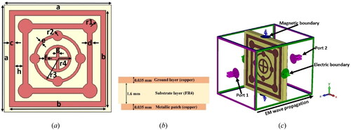
The dimensions of each segment of the resonating patch are optimized through several simulations using the model developed in CST studio suite-2019[Citation44] simulation software to attain maximum absorption at the desired resonance frequencies.[Citation45] The simulation is conducted within the frequency range of 2–8 GHz. The excitation power is supplied to the unit cell through the waveguide port which acts as the excitation wave source. Waveguide “Port 1” is placed 11.565 mm away from the unit cell in the + z direction whereas “Port 2” is the same distance away from the backplane of the unit cell in the − z direction. The boundary conditions of the electric and magnetic fields are configured along the x and y-axis directions correspondingly. However, for EM signal propagation “open (add-space)” boundary condition is used in the z-axis direction as shown in . When the EM wave is applied from the + z direction through waveguide “Port 1,” it passes through the MMA if the impedance of the MMA matches with the free space impedance. The optimized dimensions of different segments of the resonating patch of the unit cell are presented in .
Table 1. Dimensions of different segments of the resonating patch of the unit cell’s.
The complete copper backplane’s function is to prevent electromagnetic waves from passing through the absorber by working as the ground[Citation46] whereas, the copper resonator matches its impedance with the entering electromagnetic waves to offer almost zero reflection of the waves.[Citation47] Consequently, the FR4 substrate layer of the suggested MMA absorbs the EM waves. Within the necessary frequency range, the simulation can yield the values of the frequency-dependent reflection coefficient S11(ω) and transmission coefficient S21(ω). Lastly, using EquationEquation (1)(1)
(1) , the absorption coefficient A(ω) can be computed as:[Citation48]
(1)
(1)
As the transmission is restricted by a continuous copper backplane EquationEquation (1)(1)
(1) can be modified as EquationEquation (2)
(2)
(2) to calculate the absorption coefficient:
(2)
(2)
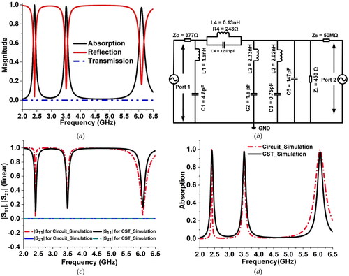
The combined absorption, reflection, and transmission phenomena of can indicate the perfect absorption at the resonances whereas the reflection coefficient decreases from unity to near zero and the transmission of the EM signal through the absorber is zero because of the use of copper backplane. The equivalent impedances of various branches of the MMA are depicted through the equivalent circuit as shown in . Based on the concept of the transmission line theory[Citation49] the equivalent circuit of the MMA is developed which contains the impedances of different segments of the MMA, transmitting port (Port 1), and receiving port (Port 2). In this circuit, a free space impedance, is presented between Port 1 and the resonator of the absorber. An inductance L1 is formed due to the presence of a metallic outer rectangular ring of the resonator whereas the capacitance C1 is formed due to the dielectric separation involving this ring and the backplane. Correspondingly, L2 represents the inductance of the second rectangular ring with bubbles and C2 is formed involving this ring and the backplane. Likewise, L3 signifies the inductance of the third circular ring with bubbles and C3 is formed for this ring and the backplane. Moreover, the coplanner inductance and its internal resistance are indicated by L4 and R4, respectively whereas the coplanner capacitance is denoted by C4. Furthermore, the combined capacitance between the innermost ring and other rings is indicated by C5. As most of the incident power is absorbed by the substrate layer, this action of the MMA is represented by an equivalent impedance of ZL. The signal transmission is blocked due to the presence of a metallic backplane in a perfect MMA which is equivalent to the phenomena of an open circuit. For this equivalent circuit design, the open circuit action is represented by a very high impedance ZB. The Advanced Design System (ADS)-19 software is used to develop the equivalent circuit diagram of where the values of inductance and capacitance of different branches are adjusted by starting from the initial values of 1 nH and 1 pF correspondingly to get the desired resonances and peak absorption values. Then the linear magnitudes of S11 and S21 acquired from the optimized equivalent circuit are jointly presented in with the S11 and S21 generated through the 3D structural simulation in CST-2019. The absorption values of the MMA for these two simulation approaches are shown combinedly in . The equivalent circuit responses of S11 and S21 are tuned independently by changing the impedances of different branches. The value of impedance ZB is responsible for controlling the magnitude of S21 and the variation of which does not affect the resonances of S11. However, the remaining circuit components help to regulate the resonances and magnitudes of S11. Particularly, the value of ZL has a decisive role in regulating S11. The close matching concerning the results of S11, S21, and absorption level for the CST simulation and ADS simulation can signify the correctness of the equivalent circuit for the MMA.
Figure 2. (a) The combined presentation of absorption, reflection, and transmission phenomena, (b) equivalent impedances of different branches, (c) magnitudes of S11 and S21 for CST and ADS simulations, and (d) absorption responses for CST and ADS simulations of the developed MMA.
2.1. Design stages of the developed MMA unit cell
Through the design stages shown in , the overall design of the MMA is achieved in a way that achieves perfect absorptions at 2.40 and 3.50 GHz. Furthermore, a near-perfect absorption resonance at 6.09 GHz is also achieved. All the design stages are influenced individually for the optimization of the final design. The reflection coefficients and absorption coefficients for the design stages are revealed in correspondingly. A rectangular ring resonator with a thickness of 1 mm is presented in Design-A, as shown in , and it may produce the highest absorption level of 99.57% at 2.40 GHz, as shown in . Correspondingly, the second rectangular ring resonator of Design-B can achieve an extra maximum absorption of 97.52% at 3.76 GHz, as well as an improved initial absorption maxima of 99.72% at 2.40 GHz. Because the goal of this research is to create a multiband absorber that targets application-oriented frequencies, Design-C is modified from Design-B to eventually shift the second resonance to 3.50 GHz with a peak absorption of 98.9%, in addition to the first resonance of 2.40 GHz with an improved peak absorption of 99.76%. Furthermore, by modifying Design-C, the proposed model of the metamaterial absorber can attain peak absorption of 96.7% at 6.09 GHz, in addition to the previous two resonances of 2.40 and 3.50 GHz. The plot of absorption, reflection, and transmission of the developed model is presented in . The bandwidths of the three distinct resonances are noted as 35.40, 41.60, and 100 MHz, respectively. In , the designs with resonances and highest absorption levels are presented.
Figure 3. Design stages of the developed MMA.
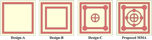
Figure 4. (a) The reflection coefficients and (b) absorption coefficients for the design stages.
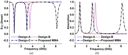
Table 2. Design stages of the MMA with resonance frequency and absorption level.
2.2. Analysis of arrays of the proposed MMA absorber
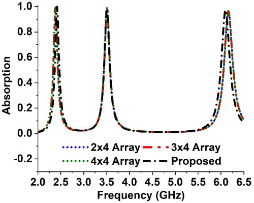
The absorption spectra of the proposed unit cell are compared with the arrays of 2 × 3, 3 × 4, and 4 × 4 of the proposed absorber as depicted in . The absorption peak of the arrays shifts toward the left side of the proposed unit cell response for 2.40 GHz. The absorptions of the arrays are changed from the absorber of the unit cell at the resonance of 3.50 GHz with unaffected frequency. In contrast to the unit cell, the third resonance frequency for arrays moves to the right. It can be observed from that there is a slight discrepancy between the absorptions of the unit cell and the arrays. This is possible because of the symmetrical structure of the absorber which eventually controls the coupling effects.
Figure 5. Absorption spectra for different arrays of the absorber.
3. The EMI shielding phenomena of the proposed MMA
The electromagnetic interference (EMI) shielding phenomena of the proposed MMA can be recognized by a parameter known as shielding effectiveness (SE) which is the combined impact of shielding effectiveness due to transmission, reflection, and multiple reflections. The multiple reflection term of SE can be neglected if the value is higher than −10 dB.[Citation50] In the logarithmic scale the value of shielding effectiveness, SE (dB) is the key indicator of a perfect electromagnetic interference shielding mechanism. With the calculation and analysis of this value using the following equation, the shielding ability of the proposed MMA of EMI can be realized:[Citation33,Citation51,Citation52]
(3)
(3)
Where the incident and transmitted filed components are represented by EI and ET correspondingly. For the proposed absorber the transmission component of SE is very close to infinity and remains almost constant throughout the entire frequency range, as the signal transmission is blocked by the copper back plate. The total SE of the absorber is dominated by the reflection component of the absorber. The larger value of the SE (dB) is the indicator of smaller energy transfer through the proposed absorber[Citation53] i.e., the proposed MMA can work as a perfect EMI shield. The commercial value of SE (dB) for the proposed MMA should be higher than 20 dB to be recognized as a potential dominant EMI shield.[Citation29] Using EquationEquation (3)(3)
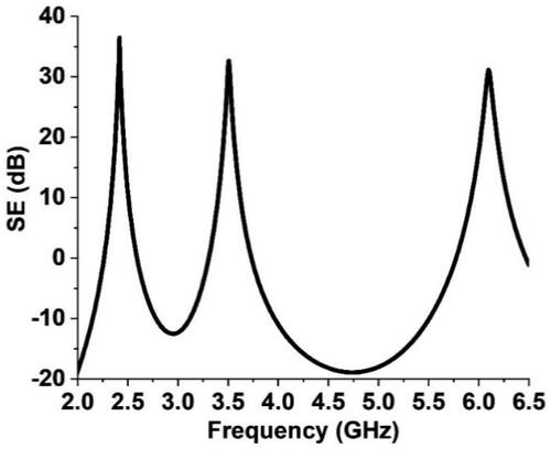
(3) the simulated response of SE (dB) due to reflection is plotted in . The high values of SE (dB) of the proposed absorber are observed at 36.44, 32.58, and 31.13 dB at the peak absorption frequencies of 2.40, 3.50, and 6.09 GHz correspondingly, which are higher than the commercial value of 20 dB.
Figure 6. Total shielding effectiveness SE (dB) of the proposed MMA.
4. Parametric study
In this section, the on-design frequency-tuning characteristic of the developed MMA is analyzed by changing the dimension and position of different bubble-shaped segments of the resonator.
4.1. Impact of simultaneous radii change of second (outer) bubble-shaped structures of the resonator
A close-up view of one of the four bubbles of the second rectangular ring of the resonator is exhibited in . The radii of these structures are considered as r1, and the corresponding data are specified in . The variation of r1 from 0.8 to 1.6 mm can influence the frequency shift of first and third resonances whereas the absorption levels are unmoved. However, the second peak absorption frequency shifted from 3.7 to 3.43 GHz with the corresponding improved absorption level from 96.8 to 99.16% which is observed in . The reason behind this frequency shifting phenomenon of the second resonance toward the lower frequency with improved absorption performance is the enhancement of resonator area toward the outer ring that is visualized by the distribution of the absolute values of the electric field, and the magnetic field,
as shown in . For the lower value of r1 = 0.8 mm and higher value of r1 = 1.6 mm, the corresponding resonances are obtained at 3.7 and 3.43 GHz. Therefore, the spreading of
at these two resonances are presented in , respectively whereas the spreading of
are presented in , respectively. All four outer bubbles along with the vertical parts of the second rectangular ring, are responsible for the resonance due to the electric field and the horizontal parts of the second rectangular ring resonating segment are responsible for the resonance due to the magnetic field. A strong distribution of
is observed for the enlargement of the area of four outer bubbles as depicted in . However electric and magnetic fields at other parts of the second rectangular ring resonator have minimum impact on the variation of the dimension of r1.
Figure 7. Absorption spectra within 3.2–4.0 GHz for changing the value of radius r1 of bubbles of the second rectangular ring.
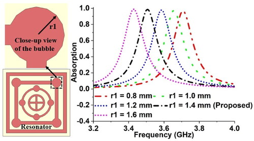
Figure 8. Distributions of the absolute values of the electric field, |E| for: (a) r1 = 0.8 mm (resonance at 3.7 GHz), (b) r1 = 1.6 mm (resonance at 3.43 GHz), and the absolute values of the magnetic field, |H| for: (c) r1 = 0.8 mm (resonance at 3.7 GHz), (d) r1 = 1.6 mm (resonance at 3.43 GHz).
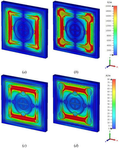
Table 3. Absorption for various radii of the second (outer) bubble-shaped structure.
4.2. Impact of simultaneous radii change of third (inner) bubble-shaped structure of the resonator
The close-up view of one of the bubbles of the third circular ring of the resonator and absorption spectra for the radius r2 change within 0.5–1.2 mm is shown in and the corresponding data are specified in . For the first and second resonance frequencies, the variation in r2 has no effect on the absorption level; however, for the third resonance, it showed the phenomenon of frequency switching. For the close observation, only the absorption spectra from 5.0 to 7.0 GHz are depicted in . There has been a frequency shift from 6.55 to 5.65 GHz for the r2 variation from 0.5 to 1.2 mm and also increases the absorption. The reason behind this phenomenon is the enlargement of the area near the circular ring resonator that controls the third resonance frequency. The influences of the electric field and magnetic field can be observed by their and
distributions at 6.55 and 5.65 GHz, respectively. The distributions of absolute values of the electric field
at these two resonances are presented in , respectively whereas the magnetic field,
distributions are presented in , respectively. The left and right portions including the attached bubbles in those portions of the circular ring and the upper and lower portions including the attached bubbles in those portions of the circular ring are responsible for the simultaneous electric field and magnetic field resonances. The
values have played a dominating role in controlling the peak absorption level and third resonance frequency. The strength of the electric field distribution is increased around the outer part of the bubble’s left and right portions of the circular ring, which can be seen in .
Figure 9. Absorption spectra within 5.2–7.0 GHz for changing the value of radius r2 of bubbles of the third circular ring.
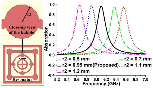
Figure 10. Distributions of the absolute values of the electric field, |E| for: (a) r2 = 0.5 mm (resonance at 6.55 GHz), (b) r2 = 1.2 mm (resonance at 5.65 GHz), and distributions of the absolute values of the magnetic field |H| for: (c) r2 = 0.5 mm (resonance at 6.55 GHz), (d) r2 = 1.2 mm (resonance at 5.65 GHz) of the MMA.
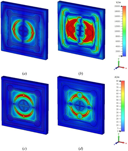
Table 4. Absorption for various radii of the third (inner) bubble-shaped structures loaded ring.
4.3. Impact of simultaneously changing the position of bubbles of the second rectangular ring resonator in the anticlockwise direction
In the section, the frequency switching behavior for the simultaneous change of positions of bubbles of the second rectangular ring resonator in the anti-clockwise direction is analyzed which is as shown in . For the P1 position of centers configuration the centers are shifted 2 mm, for P2 the centers are shifted 3 mm, for P3 the centers are shifted 4 mm, for P4 the centers are shifted 6 mm, for P5 the centers are shifted 8 mm and for P6 the centers are shifted 10 mm from their original position as presented in the proposed MMA. The first resonance frequency and the corresponding absorption level are mostly unaffected by the position variations of the centers as shown in . But for the second resonance frequency, the position configuration from P1 to P3 has a second resonance frequency changed from 3.65 to 3.61 GHz with absorption level reduction from 97.4 to 95.73% however, from P5 to P6 have second resonance frequency increased from 3.61 to 3.66 GHz with absorption level boosted from 97.46 to 98.6% as indicated in . Whereas for the third resonance frequency, the position configuration from P1 to P3 has a frequency decreased from 6.14 to 6.06 GHz with an absorption level increase from 96.75 to 99.06% on the other hand, from P5 to P6 have third resonance frequency increased from 6.06 to 6.14 GHz with absorption level drop from 99.04 to 96.6% as specified in . The distinct response is noted for configuration P4 where only two resonance frequencies are attained at 2.41 and 4.34 GHz with peak absorption of 99.78 and 93.96%, respectively. The first resonance is quite similar to the other position configurations, but the second resonance is unique. The reason behind this behavior is that overlapping of the bubbles of the rectangular ring with the bubbles of the circular ring has provided a substantial alteration of mutual inductance between these two rings that eventually developed a peak absorption of 93.96% at 4.34 GHz as well.
Figure 11. Simultaneous change of position of centers of bubbles of second rectangular ring resonator for: (a) P1 = 2 mm, (b) P2 = 3 mm, (c) P3 = 4 mm, (d) P4 = 6 mm, (e) P5 = 8 mm, and (f) P6 = 10 mm in the counterclockwise direction.
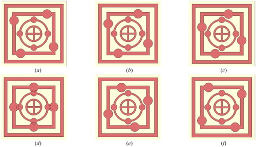
Figure 12. Absorption spectra for simultaneous change of position of centers of bubbles of the second rectangular ring resonator.
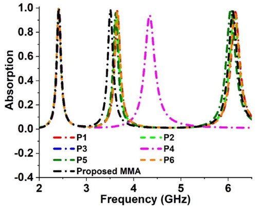
Table 5. Absorption for simultaneous change of position of centers of bubbles of second rectangular ring resonator.
5. Result analysis and discussion
5.1. Surface current analysis
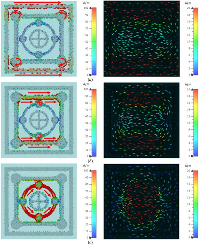
The realization of the physical behavior of the designed MMA can be justified by the movements of the front and back (ground) surface currents. The surface current movements of these two faces are shown in for three resonances of 2.40, 3.50, and 6.09 GHz correspondingly. At 2.40 GHz, the front surface current drifts from the left toward the right side (clockwise) through the upper part and also from the left to the right side (anti-clockwise) through the lower part of the most outer rectangular ring resonator. However, the ground surface current is flowing through the same spots of that plane but in opposite directions, as shown in . At 3.50 GHz, the front surface current is traveling from the left to right side (clockwise) through the upper part and inner portions of the attached bubbles and also left side to right side (anti-clockwise) direction through the lower part of the second rectangular ring resonator and inner portions of the attached bubbles as shown in . Again the reverse directional current is also following through the backplane in this case. At 6.09 GHz, a strong front surface current is moving in a clockwise direction through the upper part and attached bubble whereas an anti-clockwise current is drifting through the lower part and attached bubble of the third circular ring resonator and similarly the ground current is flowing in an antiparallel direction for this frequency as presented in . Therefore, briefly, it can be said that for all three resonances, the front surface and ground surface currents are moving in an antiparallel direction which has caused the magnetic coupling effect in the proposed absorber.[Citation54,Citation55] However, due to the instantaneous interaction E-filed and H-field resonances enhanced the absorption performance of the absorber.
Figure 13. The distribution of surface current front and ground surfaces of designed MMA at (a) 2.4 GHz, (b) 3.5 GHz, and (c) 6.09 GHz.
5.2. Effective parameter analysis
The absorption of the developed MMA is established by analyzing the complex frequency-dependent effective permittivity and permeability
using the effective medium theory.[Citation56] Because of the metallic ground plate of the absorber, the EM waves are blocked and the transmission coefficient, S21 is considered zero. As a result, the values of εeff (ω), and μeff (ω) can be recovered through the following equations:[Citation57]
(4)
(4)
(5)
(5)
Where the free space wave number is represented by ko and the distance traveled by the incoming EM wave through the MMA is indicated by d.
The real and imaginary values of effective permittivity εeff (Re), and εeff (Im), and permeability μeff (Re), and μeff (Im) are plotted in , correspondingly, and the values of these variables at peak absorption frequency are listed in . The values of εeff (Re), and μeff (Re) cause a negative refractive index. and show that at maximum absorption frequencies, εeff (Re), and μeff (Re) are of opposite signs, indicating zero-signal transmission via the designed MMA. On the other hand, for near-perfect absorption, the values of εeff (Im) and μeff (Im) should be very high at the resonances as compared to the real parts,[Citation58] which is also recognized in .
Figure 14. (a) Effective permittivity, (b) effective permeability,
and (c) normalized impedance, Z.
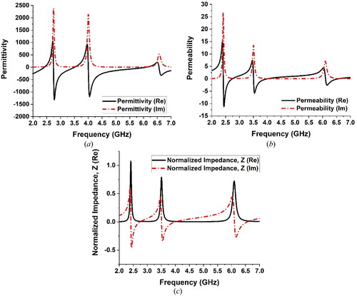
Table 6. Effective permittivity and permeability at the frequency of maximum absorption.
The dependency of absorption on the suggested absorber’s S11 is already indicated in Equation (2). The following equation depicts another relationship between S11, normalized impedance, Z, and free space impedance Z0:[Citation59]
(7)
(7)
For near-unity absorption, the reflection coefficient should be very low. This is possible if the impedance of MMA matches the free space impedance. The absorptions of the MMA at the resonances are cross-checked by the absorptions calculated using EquationEquations (1)(1)
(1) and Equation(7)
(7)
(7) which are presented in . These values of absorption perfectly matched with simulation results. The normalized impedance is presented in . For near-perfect absorption, the normalized impedance should be very close to unity and the imaginary part should be equal to zero which is satisfied for the absorption level at 2.40 GHz. As the value of normalized impedance reduced from unity, the absorption level also decreased which is indicated by the value of absorption at the frequencies of 3.50 and 6.09 GHz.
Table 7. Normalized impedances at the frequency of maximum absorption.
5.3. Polarization insensitivity analysis
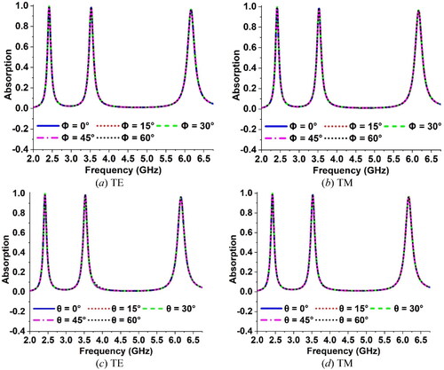
represent the direction of propagation of EM waves for transverse electric (TE) and transverse magnetic (TE) modes, respectively. In TE mode electric field vector Ez = 0, whereas in TM mode magnetic field vector Hz = 0. The polarization indifferent characteristic of the designed MMA is verified by setting the direction of wave propagation in the Z-axis direction and the polarization angle (Φ) varied from 0 to 60° with an intermission of 15° and the absorption spectra are plotted for the angular variation which can be seen from for TE mode and TM mode correspondingly. After that the incident angle (θ) is changed from 0 to 60° with an intermission of 15° and the absorption spectra are plotted for the angular variation which can be seen in for TE mode and TM mode, respectively. The absorption spectra of the TE mode perfectly match the spectra of the TM model for polarization angle variation. Similarly, the absorption spectra of TE mode perfectly match the spectra of the TM model for the incident angle variation. This means the designed absorber exhibits polarization indifferent behavior for both polarization angle and incident angle deviation. The cause behind this phenomenon is the symmetrical design of the absorber.[Citation60]
Figure 15. The directions of electric field (E) and magnetic field (H) for: (a) TE mode and (b) TM mode.
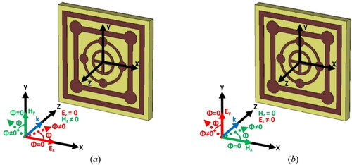
Figure 16. Absorption spectra for: (a) polarization angle (Φ) variation under TE mode, (b) polarization angle (Φ) variation under TM mode, (c) incident angle (θ) variation under TE mode, and (d) incident angle (θ) variation under TM mode.
5.4. Polarization conversion ratio analysis
The perfect absorption phenomena of the designed MMA for different orientations of incident EM waves can also be validated by the polarization conversion ratio (PCR) of the absorber. This value indicates whether an absorber works as a perfect absorber or polarization converter. For high absorption phenomena, the PCR value should be very low (near zero). The PCR value of the designed MMA is extracted using EquationEquation (8)(8)
(8) as presented in Ref.:[Citation61]
(8)
(8)
Where,
and
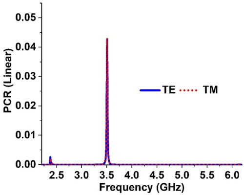
From , it is observed that the PCR values at three distinct resonances are very close to zero for both TE and TM modes of excitation which indicates high absorption with the polarization-indifferent behavior of the designed absorber. This is possible due to the structural symmetry of the designed unit cell of the absorber.
Figure 17. PCR analysis of the proposed MMA.
5.5. Measurement and simulation result analysis
The prototype of the unit cell and array of the designed MMA are fabricated on an FR4 substrate where the copper material is used for the resonator and backplane. For measurement flexibility, alongside the unit cell, the array of and
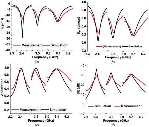
are also fabricated. To justify the simulation results and compare with the measurement results of the prototype, a measurement setup with waveguide ports is frequently used which can provide measurement flexibility, cost-effectiveness, and reasonably good accuracy compared with the free-space measurements.[Citation30] The measurement setup with a vector network analyzer (VNA), waveguide adapter, unit cell, and arrays of the proposed MMA are presented in . The measured values of reflection coefficient S11 are collected for the operating frequency ranges and using these values the absorption level and the shielding effectiveness of the fabricated metamaterial absorber are determined. The comparative plots of measurement and simulated spectra of reflection coefficient S11 in dB and linear scale, absorption, and shielding effectiveness are in . Separate waveguide adapters are used for the measurement purpose of the designed prototypes, and for that reason, continuous results are not obtained from the measurement. Thus, to present the results concisely, measurement data of S11, absorption, and SE are presented and compared with the simulation data in an interval manner instead of continuous spectra. The measurement values of S11 are noted as −12.47, −12.01, and −13.89 dB at 2.40, 3.50, and 6.09 GHz correspondingly as shown in . The corresponding linear values of S11 are presented in . It is observed that at 2.40 GHz the measured peak absorption deviated 5.52% from the simulation result, at 3.50 GHz the deviation is 10% and at 6.09 GHz the deviation is 0.8%. The measured data presented in have a significant level of similarities to the simulated results with small differences which have occurred due to some measurement aspects. The slight discrepancies have occurred due to the scum and roughness of the substrate of the prototype,[Citation62,Citation63] fabrication inaccuracy,[Citation64] coaxial cable power loss, and coupling effects of the waveguide ports. In addition, the lower cross-section area of the fabricated prototype compared to the waveguide cross-section area has an impact on measurement performance,[Citation30] Despite the small differences, high measured peak absorptions of 94.33, 88.74, and 95.92% are found at the corresponding frequencies of 2.40, 3.50, and 6.09 GHz as exhibited in . The measurement and simulation results of the shielding effectiveness of the proposed MMA are also presented in . The discrepancies in the measurement results of S11 may have influenced the SE results. The SE at three resonance frequencies have been measured at 29.15, 28.83, and 30.15 dB, respectively which are still higher than the minimum commercial value of SE of 20 dB, and these values also have proximity with the simulation results of 36.44, 32.58, and 31.13 dB, respectively. So, the proposed MMA can be employed to provide EMI shielding against Wi-Fi and 5G signals.
Figure 18. Measurement setup of the proposed MMA with VNA and waveguide adapter setup.
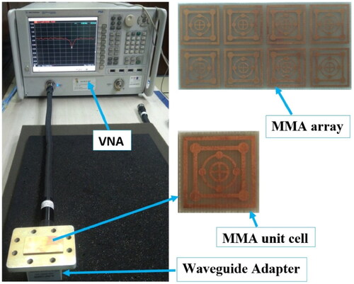
Figure 19. The comparative plots of measurement and simulated spectra of (a) S11 in dB, (b) S11 in linear scale, (c) absorption, and (d) shielding effectiveness.
A comparative assessment based on the performance features of the proposed frequency tunable bubble-shaped structure loaded MMA and information from the recent related research articles is accumulated in . The use of FR4 material as the substrate of Refs.[Citation4,Citation67,Citation68] including our designed absorber can provide a cost-effective solution whereas Neoprene rubber is used in Ref.[Citation65] and PET, PMMA, and Quartz glass are utilized in Ref.[Citation66] The absorption level of the developed MMA is higher at three different frequencies of peak absorption than most of the research works indicated in except for the design of Ref.[Citation68] which only focuses on single resonance frequency. As the feature presented in Refs.,[Citation4,Citation65–68] our developed MMA can also demonstrate polarization insensitivity for the structural uniformity of the design. As a result, it can be effectively used for sensing and detection applications. The frequency tunable feature of the proposed MMA is achieved through the dimension change of different segments as explained in the parametric study section. The frequency tunable feature is also observed in Refs.,[Citation4,Citation66] however, this feature is missing in Refs.[Citation65,Citation67,Citation68] Besides near unity absorption, the proposed absorber can provide excellent shielding effectiveness at three distinct frequencies which are not analyzed in other research work mentioned in except Ref.[Citation66] From the above discussion, it is obvious that the metamaterial-based designs of the relevant research articles are not focused on any particular frequency of operation as the proposed design of the MMA. In addition, the proposed design has the explicit advantage over the recent related research works of executing high SE and near-unity absorption at the frequencies of 2.40 and 3.50 GHz that can be implemented in the Wi-Fi and WiMAX devices, respectively along with additional frequency application of 6.09 GHz. Moreover, the proposed model can provide on-design frequency switching properties within 3.43–3.7 and 5.65–6.55 GHz with the help of dimension change of bubble-shaped structures loaded on the second and third rings of the absorber.
Table 8. Assessment of proposed MMA in comparison with the recent relevant research articles.
6. Conclusion
In this paper, bubble-shaped structures loaded resonator-based metamaterial absorber is developed to cover the frequencies of 2.40 and 3.50 GHz used in conventional communication applications in addition to 6.09 GHz, which can absorb the EM signals of Wi-Fi and 5G communication devices. The designed MMA can absorb near-perfect absorption of 99.85, 98.6, and 96.7% at these peak absorption frequencies. The simulation results of the model have a strong resemblance with the measurement results. The absorption phenomena are investigated by the surface current movement at the resonance frequencies, which is also endorsed by the analysis of the effective parameters of the developed model. In addition, simulated values of 36.44, 32.58, and 31.13 dB and measured values of 29.15, 28.83, and 30.15 dB of shielding effectiveness at the corresponding resonance frequencies are significantly larger than the values of 20 dB (minimum requirement for commercial use), which has encouraged the application of our MMA for shielding against the electromagnetic interferences of Wi-Fi and 5G communication devices. The structural symmetry of the designed MMA helps to demonstrate the stable operation in both TE and TM modes for the variation of polarization and incident angle up to 60°, which are further supported by the PCR analysis near zero value to act as the near-perfect absorber. Moreover, the changing dimension of the bubble-shaped structures loaded on the second and third rings of the absorber helped the frequencies tune within 3.43–3.7 and 5.65–6.55 GHz which may allow the metamaterial absorber to extend its applications in Wi-MAX. and RFID devices.
| Nomenclature | ||
| Wireless Fidelity | = | (Wi-Fi) |
| Fifth Generation | = | (5G) |
Author contributions
Abdullah Al Mahfazur Rahman: conceptualization, formal analysis, methodology, design, investigation, writing-original draft. Mohammad Tariqul Islam: methodology, supervision, project administration, software, review and editing, and funding acquisition. Md. Moniruzzaman: conceptualization, methodology, design, investigation, review and editing. Haitham Alsaif: data curation, investigation, review and editing, and funding acquisition. Abdulwadoud A. Maash: data curation, validation, review and editing, and funding acquisition. Md. Mhedi Hasan: data curation, visualization, review, and editing. Mohamed S. Soliman: data curation, investigation, review and editing, and funding acquisition.
Additional information
Funding
References
- Du, Z.; Liang, J.; Cai, T.; Wang, G.; Deng, T.; Wu, B. Designing an ultra-thin and wideband low-frequency absorber based on lumped resistance. Opt. Express 2022, 30, 914–925. DOI: 10.1364/OE.445081.
- Misran, N.; Hafizah Yusop, S.; Islam, M. T.; Ismail, M. Y. Analysis of parameterization substrate thickness and permittivity for concentric split ring square reflectarray element. J. Eng. 2012, 23, 11–16.
- Tirkey, M. M.; Gupta, N. Broadband polarization-insensitive inkjet-printed conformal metamaterial absorber. IEEE Trans. Electromagn. Compat. 2021, 63, 1829–1836. DOI: 10.1109/TEMC.2021.3089830.
- Dhillon, A. S.; Mittal, D.; Bargota, R. Triple band ultrathin polarization insensitive metamaterial absorber for defense, explosive detection and airborne radar applications. Micro. Opt. Tech. Lett. 2019, 61, 89–95. DOI: 10.1002/mop.31547.
- Rahman, A. A. M.; Islam, M. T.; Moniruzzaman, M.; Rahim, S. K. A.; Singh, M.; Misran, N.; Islam, M. S.; Soliman, M. S. H-shaped modifiers loaded mirror symmetric resonator based double negative metamaterial for multi-band wireless communications. Sci. Rep. 2023, 13, 15943. DOI: 10.1038/s41598-023-43182-y.
- Moniruzzaman, M.; Tariqul Islam, M.; Fais Mansor, M.; Soliman, M. S.; Misran, N.; Samsuzzaman, M. Tuning metallic stub loaded symmetrical resonator based dual band metamaterial absorber for wave shielding from Wi-Fi frequencies. Alexandria Eng. J. 2023, 63, 399–414. DOI: 10.1016/j.aej.2022.07.051.
- Qiu Xu, Y.; Heng Zhou, P.; Bin Zhang, H.; Chen, L.; Jiang Deng, L. A wide-angle planar metamaterial absorber based on split ring resonator coupling. J. Appl. Phys. 2011, 110, 044102. DOI: 10.1063/1.3622675.
- Costa, F.; Monorchio, A.; Manara, G. Theory, design and perspectives of electromagnetic wave absorbers. IEEE Electromagn. Compat. Mag. 2016, 5, 67–74. DOI: 10.1109/MEMC.0.7543954.
- Ünal, E.; Bağmancı, M.; Karaaslan, M.; Akgol, O.; Sabah, C. Strong absorption of solar energy by using wide band metamaterial absorber designed with plus-shaped resonators. Int. J. Mod. Phys. B 2018, 32, 1850275. DOI: 10.1142/S0217979218502752.
- Stantchev, R. I.; Phillips, D. B.; Hobson, P.; Hornett, S. M.; Padgett, M. J.; Hendry, E. Compressed sensing with near-field THz radiation. Optica 2017, 4, 989–992. DOI: 10.1364/OPTICA.4.000989.
- Choudhary, Y. S.; Gomathi, N. Metamaterials as shielding materials. In Advanced Materials for Electromagnetic Shielding: Fundamentals, Properties, and Applications. John Wiley & Sons, USA, 2018; pp. 367–391.
- Yang, Q.; Xiong, H.; Deng, J.-H.; Wang, B.-X.; Peng, W.-X.; Zhang, H.-Q. Polarization-insensitive composite gradient-index metasurface array for microwave power reception. Appl. Phys. Lett. 2023, 122, 253901. DOI: 10.1063/5.0155547.
- Chen, M.; Singh, L.; Xu, N.; Singh, R.; Zhang, W.; Xie, L. Terahertz sensing of highly absorptive water-methanol mixtures with multiple resonances in metamaterials. Opt. Express 2017, 25, 14089–14097. DOI: 10.1364/OE.25.014089.
- Moniruzzaman, M.; Islam, M. T.; Muhammad, G.; Singh, M. S. J.; Samsuzzaman, M. Quad band metamaterial absorber based on asymmetric circular split ring resonator for multiband microwave applications. Results Phys. 2020, 19, 103467. DOI: 10.1016/j.rinp.2020.103467.
- Xiong, H.; Ma, X.; Liu, H.; Xiao, D.; Zhang, H. Research on electromagnetic energy absorption and conversion device with four-ring multi-resistance structure. Appl. Phys. Lett. 2023, 123, 153902. DOI: 10.1063/5.0170827.
- Xiong, H.; Ma, X.; Wang, B.-X.; Zhang, H. Design and analysis of an electromagnetic energy conversion device. Sens. Actuators A 2024, 366, 114972. DOI: 10.1016/j.sna.2023.114972.
- Deng, J.-H.; Xiong, H.; Yang, Q.; Suo, M.; Xie, J.-Y.; Zhang, H.-Q. Metasurface-based microwave power detector for polarization angle detection. IEEE Sens. J. 2023, 23, 22459–22465. DOI: 10.1109/JSEN.2023.3306462.
- Xiong, H.; Deng, J.; Yang, Q.; Wang, B.-X.; Wang, X.; Zhang, H. A metamaterial energy power detector based on electromagnetic energy harvesting technology. ACS Appl. Electron. Mater. 2024, 6, 1204–1210. DOI: 10.1021/acsaelm.3c01578.
- Cai, B.; Wu, L.; Zhu, X.; Cheng, Z.; Cheng, Y. Ultra-broadband and wide-angle plasmonic light absorber based on all-dielectric gallium arsenide (GaAs) metasurface in visible and near-infrared region. Results Phys. 2024, 58, 107509. DOI: 10.1016/j.rinp.2024.107509.
- Wu, L.; Yang, L.; Zhu, X.; Cai, B.; Cheng, Y. Ultra-broadband and wide-angle plasmonic absorber based on all-dielectric gallium arsenide pyramid nanostructure for full solar radiation spectrum range. Int. J. Therm. Sci. 2024, 201, 109043. DOI: 10.1016/j.ijthermalsci.2024.109043.
- Cheng, Y.; Qian, Y.; Luo, H.; Chen, F.; Cheng, Z. Terahertz narrowband perfect metasurface absorber based on micro-ring-shaped GaAs array for enhanced refractive index sensing. Physica E 2023, 146, 115527. DOI: 10.1016/j.physe.2022.115527.
- Cheng, Y.; Zhao, J. Simple design of a six-band terahertz perfect metasurface absorber based on a single resonator structure. Phys. Scr. 2022, 97, 095508. DOI: 10.1088/1402-4896/ac8ad6.
- Rong, C.; Cai, B.; Cheng, Y.; Chen, F.; Luo, H.; Li, X. Dual-band terahertz chiral metasurface absorber with enhanced circular dichroism based on temperature-tunable InSb for sensing applications. Phys. Chem. Chem. Phys. 2024, 26, 5579–5588. DOI: 10.1039/D3CP05528K.
- Wang, B.-X.; Duan, G.; Lv, W.; Tao, Y.; Xiong, H.; Zhang, D.-Q.; Yang, G.; Shu, F.-Z. Design and experimental realization of triple-band electromagnetically induced transparency terahertz metamaterials employing two big-bright modes for sensing applications. Nanoscale 2023, 15, 18435–18446. DOI: 10.1039/d3nr05095e.
- Thomassin, J.-M.; Jérôme, C.; Pardoen, T.; Bailly, C.; Huynen, I.; Detrembleur, C. Polymer/carbon based composites as electromagnetic interference (EMI) shielding materials. Mater. Sci. Eng. R Rep. 2013, 74, 211–232. DOI: 10.1016/j.mser.2013.06.001.
- Kausar, A.; Rafique, I.; Muhammad, B. Electromagnetic interference shielding of polymer/nanodiamond, polymer/carbon nanotube, and polymer/nanodiamond–carbon nanotube nanobifiller composite: A review. Polym. Plast. Technol. Eng. 2017, 56, 347–363. DOI: 10.1080/03602559.2016.1233273.
- Zhang, L.; Li, X.; Jiao, X.; Li, J.; Toor, S. S.; Bhobe, A. U.; Pommerenke, D. J.; Drewniak, J. L. EMI coupling paths and mitigation in optical transceiver modules. IEEE Trans. Electromagn. Compat. 2017, 59, 1848–1855. DOI: 10.1109/TEMC.2017.2697761.
- Chen, H.; Huang, Z.; Huang, Y.; Zhang, Y.; Ge, Z.; Qin, B.; Liu, Z.; Shi, Q.; Xiao, P.; Yang, Y.; et al. Synergistically assembled MWCNT/graphene foam with highly efficient microwave absorption in both C and X bands. Carbon 2017, 124, 506–514. DOI: 10.1016/j.carbon.2017.09.007.
- Wei, Q.; Pei, S.; Qian, X.; Liu, H.; Liu, Z.; Zhang, W.; Zhou, T.; Zhang, Z.; Zhang, X.; Cheng, H.; et al. Superhigh electromagnetic interference shielding of ultrathin aligned pristine graphene nanosheets film. Adv. Mater. 2020, 32, 1907411. DOI: 10.1002/adma.201907411.
- Cheng, Y.; Qian, Y.; Homma, H.; Fathnan, A. A.; Wakatsuchi, H. Waveform-selective metasurface absorber with a single-patch structure and lumped nonlinear circuit for a higher-order mode. IEEE Trans. Antennas Propag. 2023, 71, 8677–8691. DOI: 10.1109/TAP.2023.3308581.
- Zhou, J.; Bie, S.; Wan, D.; Xu, H.; Xu, Y.; Jiang, J. Realization of thin and broadband magnetic radar absorption materials with the help of resistor FSS. Antennas Wirel. Propag. Lett. 2015, 14, 24–27. DOI: 10.1109/LAWP.2014.2349533.
- Yan, M.; Qu, S.; Wang, J.; Zhang, J.; Zhou, H.; Chen, H.; Zheng, L. A miniaturized dual-band FSS with stable resonance frequencies of 2.4 GHz/5 GHz for WLAN applications. Antennas Wirel. Propag. Lett. 2014, 13, 895–898. DOI: 10.1109/LAWP.2014.2320931.
- Syed, I. S.; Ranga, Y.; Matekovits, L.; Esselle, K. P.; Hay, S. G. A single-layer frequency-selective surface for ultrawideband electromagnetic shielding. IEEE Trans. Electromagn. Compat. 2014, 56, 1404–1411. DOI: 10.1109/TEMC.2014.2316288.
- Wang, B.-X.; Zhai, X.; Wang, G.-Z.; Huang, W.-Q.; Wang, L.-L. Frequency tunable metamaterial absorber at deep-subwavelength scale. Opt. Mater. Express 2015, 5, 227–235. DOI: 10.1364/OME.5.000227.
- Wu, T.; Li, W.; Chen, S.; Guan, J. Wideband frequency tunable metamaterial absorber by splicing multiple tuning ranges. Results Phys. 2021, 20, 103753. DOI: 10.1016/j.rinp.2020.103753.
- Xu, J.; Wang, J.; Yang, R.; Tian, J.; Chen, X.; Zhang, W. Frequency-tunable metamaterial absorber with three bands. Optik 2018, 172, 1057–1063. DOI: 10.1016/j.ijleo.2018.07.125.
- Kim, H. K.; Lee, D.; Lim, S. Frequency-tunable metamaterial absorber using a varactor-loaded fishnet-like resonator. Appl. Opt. 2016, 55, 4113–4118. DOI: 10.1364/AO.55.004113.
- Ji, S.; Luo, Z.; Zhao, J.; Dai, H.; Jiang, C. Design and analysis of an ultra-thin polarization-insensitive wide-angle triple-band metamaterial absorber for X-band application. Opt. Quant. Electron. 2021, 53, 1–19. DOI: 10.1007/s11082-021-02760-y.
- Zhao, J.; Cheng, Y. Ultrabroadband microwave metamaterial absorber based on electric SRR loaded with lumped resistors. J. Electron. Mater. 2016, 45, 5033–5039. DOI: 10.1007/s11664-016-4693-0.
- Bilal, R. M. H.; Baqir, M. A.; Choudhury, P. K.; Karaaslan, M.; Ali, M. M.; Altlntas, O.; Rahim, A. A.; Unal, E.; Sabah, C. Wideband microwave absorber comprising metallic split-ring resonators surrounded with e-shaped fractal metamaterial. IEEE Access 2021, 9, 5670–5677. DOI: 10.1109/ACCESS.2020.3048927.
- Bait-Suwailam, M. M. Electromagnetic field interaction with metamaterials. In Electromagnetic Fields and Waves. IntechOpen Limited, London, UK, 2019; pp. 1–19.
- Pozar, D. M. Microwave Engineering: Theory and Techniques. John Wiley & Sons, USA, 2021.
- Rahman, A. A. M.; Islam, M. T.; Moniruzzaman, M.; Misran, N.; Alorifi, F.; Shamsan, Z. A.; Almuhanna, K.; Rahim, S. K. A.; Islam, M. S.; Soliman, M. S. Triple band frequency tunable polarization insensitive metamaterial absorber for WLAN and 5G applications. Opt. Mater. 2023, 145, 114368. DOI: 10.1016/j.optmat.2023.114368.
- Systèmes, D. CST Studio Suite Help. Dassault Systèmes: Waltham, MA, 2019.
- Moniruzzaman, M.; Islam, M. T.; Misran, N.; Samsuzzaman, M.; Alam, T.; Chowdhury, M. E. H. Inductively tuned modified split ring resonator based quad band epsilon negative (ENG) with near zero index (NZI) metamaterial for multiband antenna performance enhancement. Sci. Rep. 2021, 11, 11950. DOI: 10.1038/s41598-021-91432-8.
- Hasan, M. S.; Islam, M. T.; Samsuzzaman, M.; Alamri, S.; Albadran, S.; Moniruzzaman, M.; Soliman, M. S. Double elliptical resonator based quad-band incident angle and polarization angle insensitive metamaterial absorber for wireless applications. Opt. Laser Technol. 2024, 171, 110334. DOI: 10.1016/j.optlastec.2023.110334.
- Zakir, S.; R. M. H.; Bilal, M. A.; Naveed, M. A.; Baqir, Muhammad, U.; Ali Khan, M. M.; Ali, M. A.; Saeed, M. Q.; Mehmood.; Y.; Massoud. Polarization-insensitive, broadband, and tunable terahertz absorber using slotted-square graphene meta-rings. IEEE Photon. J. 2023, 15, 1–8. DOI: 10.1109/JPHOT.2022.3229900.
- Holloway, C. L.; Kuester, E. F.; Gordon, J. A.; O'Hara, J.; Booth, J.; Smith, D. R. An overview of the theory and applications of metasurfaces: The two-dimensional equivalents of metamaterials. IEEE Antennas Propag. Mag. 2012, 54, 10–35. DOI: 10.1109/MAP.2012.6230714.
- Assimonis, S. D.; Fusco, V. Polarization insensitive, wide-angle, ultra-wideband, flexible, resistively loaded, electromagnetic metamaterial absorber using conventional inkjet-printing technology. Sci. Rep. 2019, 9, 12334. no DOI: 10.1038/s41598-019-48761-6.
- Dhawan, S. K.; Singh, A. P.; Ohlan, A. Smart Materials Design for Electromagnetic Interference Shielding Applications. Bentham Science Publishers, Singapore, 2022.
- Nauman, M.; Saleem, R.; Rashid, A. K.; Shafique, M. F. A miniaturized flexible frequency selective surface for X-band applications. IEEE Trans. Electromagn. Compat. 2016, 58, 419–428. DOI: 10.1109/TEMC.2015.2508503.
- Katoch, K.; Jaglan, N.; Gupta, S. D.; Sharawi, M. S. Design of a triple band notched polarization independent compact FSS at UWB frequency range. Int. J. RF Microw. Comput. Aided Eng. 2021, 31, e22631.
- Luo, X.; Chung, D. D. L. Electromagnetic interference shielding using continuous carbon-fiber carbon-matrix and polymer-matrix composites. Compos. Part B Eng. 1999, 30, 227–231. DOI: 10.1016/S1359-8368(98)00065-1.
- Kumari, K.; Mishra, N.; Chaudhary, R. K. An ultra‐thin compact polarization insensitive dual band absorber based on metamaterial for X‐band applications. Micro. Opt. Tech. Lett. 2017, 59, 2664–2669. DOI: 10.1002/mop.30797.
- Bhattacharya, A.; Bhattacharyya, S.; Ghosh, S.; Chaurasiya, D.; Vaibhav Srivastava, K. An ultrathin penta‐band polarization‐insensitive compact metamaterial absorber for airborne radar applications. Micro. Opt. Tech. Lett. 2015, 57, 2519–2524. DOI: 10.1002/mop.29365.
- Tak, J.; Jin, Y.; Choi, J. A dual‐band metamaterial microwave absorber. Micro. Opt. Tech. Lett. 2016, 58, 2052–2057. DOI: 10.1002/mop.29977.
- Smith, D. R.; Vier, D. C.; Koschny, T.; Soukoulis, C. M. Electromagnetic parameter retrieval from inhomogeneous metamaterials. Phys. Rev. E Stat. Nonlin. Soft Matter Phys. 2005, 71, 036617. DOI: 10.1103/PhysRevE.71.036617.
- Kalraiya, S.; Kumar Chaudhary, R.; Gangwar, R. K. Polarization independent triple band ultrathin conformal metamaterial absorber for C-and X-frequency bands. AEU-Int. J. Electron. Commun. 2021, 135, 153752. DOI: 10.1016/j.aeue.2021.153752.
- Deng, R.; Li, M.; Muneer, B.; Zhu, Q.; Shi, Z.; Song, L.; Zhang, T. Theoretical analysis and design of ultrathin broadband optically transparent microwave metamaterial absorbers. Materials 2018, 11, 107. DOI: 10.3390/ma11010107.
- Nguyen, T. T.; Lim, S. Design of metamaterial absorber using eight-resistive-arm cell for simultaneous broadband and wide-incidence-angle absorption. Sci. Rep. 2018, 8, 6633. DOI: 10.1038/s41598-018-25074-8.
- Hossain, I.; Samsuzzaman, M.; Moniruzzaman, M.; Bais, B. B.; Singh, M. S. J.; Islam, M. T. Polarization-independent broadband optical regime metamaterial absorber for solar harvesting: A numerical approach. Chin. J. Phys. 2021, 71, 699–715. DOI: 10.1016/j.cjph.2021.04.007.
- Tran, C. M.; Van Pham, H.; Nguyen, H. T.; Nguyen, T. T.; Vu, L. D.; Do, T. H. Creating multiband and broadband metamaterial absorber by multiporous square layer structure. Plasmonics 2019, 14, 1587–1592. DOI: 10.1007/s11468-019-00953-6.
- Thummaluru, S. R.; Mishra, N.; Chaudhary, R. K. Design and analysis of an ultrathin triple-band polarization independent metamaterial absorber. AEU-Int. J. Electron. Commun. 2017, 82, 508–515. DOI: 10.1016/j.aeue.2017.10.024.
- Jain, P.; Singh, A. K.; Pandey, J. K.; Garg, S.; Bansal, S.; Agarwal, M.; Kumar, S.; Sardana, N.; Gupta, N.; Singh, A. K. Ultra‐thin metamaterial perfect absorbers for single‐/dual‐/multi‐band microwave applications. IET Microw. Antennas Propag. 2020, 14, 390–396. DOI: 10.1049/iet-map.2019.0623.
- Kaur, K. P.; Upadhyaya, T.; Palandoken, M.; Gocen, C. Ultrathin dual‐layer triple‐band flexible microwave metamaterial absorber for energy harvesting applications. Int. J. RF Microw. Comput. Aided Eng. 2019, 29, e21646. DOI: 10.1002/mmce.21646.
- Zhang, Y.; Dong, H.; Mou, N.; Chen, L.; Li, R.; Zhang, L. High-performance broadband electromagnetic interference shielding optical window based on a metamaterial absorber. Opt. Express 2020, 28, 26836–26849. DOI: 10.1364/OE.401766.
- de Araujo, J. B. O.; Siqueira, G. L.; Kemptner, E.; Weber, M.; Junqueira, C.; Mosso, M. M. An ultrathin and ultrawideband metamaterial absorber and an equivalent-circuit parameter retrieval method. IEEE Trans. Antennas Propag. 2020, 68, 3739–3746. DOI: 10.1109/TAP.2020.2963900.
- Mishra, R. K.; Gupta, R. D.; Datar, S. Metamaterial microwave absorber (MMA) for electromagnetic interference (EMI) shielding in X-band. Plasmonics 2021, 16, 2061–2071. DOI: 10.1007/s11468-021-01465-y.